US4528591A - Raster scan frame digitizer method and apparatus - Google Patents
Raster scan frame digitizer method and apparatus Download PDFInfo
- Publication number
- US4528591A US4528591A US06/408,349 US40834982A US4528591A US 4528591 A US4528591 A US 4528591A US 40834982 A US40834982 A US 40834982A US 4528591 A US4528591 A US 4528591A
- Authority
- US
- United States
- Prior art keywords
- input signal
- video input
- amplitude
- values
- window
- Prior art date
- Legal status (The legal status is an assumption and is not a legal conclusion. Google has not performed a legal analysis and makes no representation as to the accuracy of the status listed.)
- Expired - Fee Related
Links
Images


Classifications
-
- H—ELECTRICITY
- H04—ELECTRIC COMMUNICATION TECHNIQUE
- H04N—PICTORIAL COMMUNICATION, e.g. TELEVISION
- H04N5/00—Details of television systems
- H04N5/14—Picture signal circuitry for video frequency region
Definitions
- the subject matter of the present invention pertains to a raster scan frame digitizer capable of digitizing an image displayed on a cathode ray tube (CRT) and storing the digital values representative of said image in a memory.
- CTR cathode ray tube
- CTR cathode-ray tube
- the image presented on the CRT must remain stationary. However, if the image is continually moving or otherwise changing, it is desirable to decrease the time required to digitize the stationary image displayed on the CRT and thereby decrease the time required for the CRT image to remain stationary.
- the stationary image may be digitized to accomplish several objectives. It may be necessary to process the image, digitally, in real time. It may also be necessary to produce hard copies of the stationary image, or it may be necessary merely to store the image in a memory for the purpose of formatting the image differently.
- CTR cathode ray tube
- a window comparator is used to compare the amplitude of the incoming video with the fixed value.
- the fixed value may, for example, be a count stored in a counter, the counter being incremented by one each time one scan of the CRT image is completed.
- the window comparator establishes a certain window, the differential voltage level of the window being a function of the count of the counter. If the amplitude of the video signal falls within the differential voltage level of the window, an output is generated from the window comparator.
- a D-type flip-flop is connected to the output of the window comparator.
- a sample clock pulse energizes the D-type flip-flop once each time a pixel on a line of the CRT is encountered during the frame scan.
- the D-type flip-flop In response to the sample clock pulse, the D-type flip-flop generates an output pulse corresponding to the output signal from the window comparator.
- the output pulse enables a RAM memory, so that a fixed value may be written therein.
- the d.c. level of the window rises from zero, the original fixed value (count) in the counter.
- the output pulse enables the RAM memory and a fixed value, a count in the counter, is written in the RAM memory.
- two or more comparisons are made between the amplitude of the video signal and a respective fixed value.
- two or more window comparators are utilized along with two or more respective D-type flip-flops, two or more respective counters and D/A converters.
- the outputs of each of the window comparators are connected to input terminals of D-type flip-flops.
- the output terminals of each of the D-type flip-flops are connected to input terminals of an OR-gate.
- the output of the OR-gate is used to enable a RAM memory.
- the count of the corresponding counter is stored in the RAM memory, the count being a fixed value representative of the amplitude of the video signal at a particular point on the CRT.
- two or more counters and two or more window comparators two or more windows are developed to digitize the video signal. Therefore, the speed at which the video signal is digitized is increased, and the time required for the CRT image to remain stationary is decreased.
- FIGS. 1a-1b are schematic representations of a window comparator used with the present invention.
- FIG. 1c is a timing waveform of the video input signal illustrated in conjunction with the window, the AND gate output, and the window comparator output of FIG. 1b.
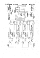
- FIG. 2 represents one preferred embodiment of the raster scan frame digitizer of the present invention.
- FIG. 3 illustrates a video input signal waveform and two windows for each frame for providing a functional explanation of the operation of the embodiment of invention shown in FIG. 2.
- FIG. 4 illustrates a video input signal waveform and three windows for each frame for providing a functional explanation of the operation of an alternative embodiment of invention.
- FIGS. 5a-5b illustrate and describe an alternative embodiment of present invention.
- FIGS. 6a-6c illustrate and describe still another alternative embodiment of present invention.
- FIGS. 7a-7b illustrate and describe still a further alternative embodiment of present invention.
- this invention is directed to an apparatus and method for digitizing a stationary image on a CRT by dividing each horizontal line of an image displayed on the CRT into "N" pixels, the video signal, if any, present at each pixel being assigned a digital value and stored in a memory. All of the horizontal lines of the CRT image collectively comprise a frame.
- the digital values stored in memory can be used to enhance or re-format the image in any manner desirable for further recreation of the image on hardcopy.
- the image displayed on the CRT must remain stationary during the digitization thereof.
- the present invention is directed to minimizing the time required to digitize the image, and thereby, to minimizing the time required for the CRT image to remain stationary.
- FIG. 1a a schematic representation of a typical window comparator 10 is illustrated. Note that there are three input terminals to the window comparator. One input terminal has applied thereto a first reference voltage VREF1. The second input terminal has applied thereto a second reference voltage VREF2. The third input terminal has applied thereto the video input signal. When the amplitude of the video input signal is greater than VREF1 but less than VREF2, an output signal is generated from the window comparator. However, if the amplitude of the video input signal lies outside the range from VREF1 to VREF2, no output signal is generated from the window comparator.
- the window comparator 10 comprises a first comparator 10A and a second comparator 10B.
- Each of the first and second comparators 10A and 10B have complementary outputs, such that when one output is high, the other output is low, and viceversa.
- the video input signal energizes the positive input terminal of both comparators.
- the negative output terminal of the first comparator 10A is connected to one input of an AND gate.
- the positive output terminal of the second comparator 10B is connected to another input of the AND gate.
- a D to A converter (16 and 16A of FIG. 2) generates an output signal which energizes the negative input terminal of the second comparator 10B.
- the output signal from the D to A converter also energizes one input terminal of a summer 10D.
- the sum of ⁇ V and the output signal from the D to A converter is applied to the negative input terminal of the first comparator 10A.
- V REF the video-in signal
- the video-in signal must also be less than V REF 2 in order that an output signal be generated from the negative output terminal of the first comparator 10A.
- the video input signal waveform is illustrated along with the window, the width of the window being the difference between VREF1 and VREF2.
- the AND gate output pulses (the window comparator output) are shown as being generated when the video input signal amplitude lies in a range between VREF1 and VREF2.
- the video input signal is applied to one input terminal of a window comparator 12.
- the output terminal of the window comparator 12 is connected to a D-type flip-flop 14.
- Sample clock pulses energize the D-type flip-flop 14. One sample clock pulse is generated each time a pixel on a line of a frame is encountered. The sample clock pulse ensures that the output signal from the D-type flip-flop 14 is high at the sample clock pulse's leading or rising edge.
- the other input terminal of window comparator 12 is connected to the output terminal of D to A converter 16.
- the input terminal of the D to A converter 16 is connected to the output terminal of an up counter 18.
- Frame clock pulses energize the up counter 18.
- the upcounter 18 In response to the clock pulse, the upcounter 18 begins its counting operation. One frame clock pulse is generated when the raster scan for each frame is initiated. The output terminal of the up counter 18 is also connected to the input terminal of a tristate buffer 20. The output terminal of the D-type flip-flop 14 is connected to an enable input terminal of the tri-state buffer 20.
- the tri-state buffer 20 may be thought of as a simple switch, wherein, when the output pulse from the D-type flip-flop is generated, the enable input terminal of the tri-state buffer 20 is energized, thereby closing the switch. The output terminal of the tri-state buffer 20 is connected to a data input terminal of a random access read/write memory 22.
- the video input signal also energizes one input terminal of a second window comparator 12a.
- the output terminal of the second window comparator 12a is connected to the input terminal of a second D-type flip-flop 14a.
- the second D-type flip-flop 14a is also energized by the sample clock pulse as mentioned hereinbefore.
- the output pulse from the second D-type flip-flop 14a is high at the sample clock pulse's rising edge.
- the other input terminal of the second window comparator 12a is connected to the output terminal of a second D to A converter 16a.
- the input terminal of the second D to A converter 16a is connected to the output terminal of a down counter 18a.
- an offset circuit 19 is connected to the down counter 18a for loading the predetermined value into the counter.
- the offset circuit 19 loads the value 2 n into the down counter 18a as its predetermined value, where "n" is the number of bits representing each pixel, the value “2 n “ defining the maximum amplitude of the video input signal.
- the down counter 18a is also energized by frame clock pulses, a frame clock pulse being generated when the raster scan for each frame is initiated.
- the output of the down counter 18a is also connected to the input of a second tri-state buffer 20a.
- the tri-state buffer 20a is also enabled by the output signal from the second D-type flip-flop 14a.
- the buffer 20a When the output signal from the D-type flip-flop 14a enables the second tri-state buffer 20a, the buffer 20a generates an output signal representative of the count in the down counter 18A, the output signal energizing the data input terminal of the random access memory 22.
- the count in counter 18A is therefore stored in RAM 22.
- the outputs from the first and second D-type flip-flops 14 and 14a, respectively, are connected to the input terminals of an OR gate 24.
- the output terminal from the OR gate 24 is connected to the write-1 input terminal of the random access memory 22.
- the pixel address counter 26 is connected to the random access memory for addressing various locations within the random access memory 22. Sample clock pulses also energize the pixel address counter 26 for initiating the addressing of the RAM by the address counter 26 each time a pixel in the frame is encountered
- FIG. 3 a video input signal for one frame is illustrated in conjunction with a multiple number of frames of the raster scan.
- the windows established by the first and second window comparators 12 and 12a, respectively are also illustrated.
- the up-counter 18 counts up from the value "0" (zero).
- 2 n is a value which is loaded into the down counter 18a by the offset circuit 19, the down counter 18a counting down from the value 2 n .
- reference is directed to frame 2. Note that the window established by the second window comparator 12a has moved down along the V axis, and the window established by the first window comparator has moved up along the V axis. Referring to frame n, the last frame, note that the windows established by the first and second window comparators 12 and 12a have merged at a point midway between the maximum and minimum values of the amplitude associated with the video input signal.
- counter 18 is set to a value approximately equal to zero.
- This counter 18 begins its count when energized by a frame clock pulse.
- the frame clock pulse occurs once each frame of the raster scan, usually at the initiation of the scan of the frame.
- the D to A converter converts the digital input signal to an analog signal at its output terminal thereof.
- the window established by the first window comparator moves up along the V-axis, shown in FIG. 3.
- an output signal is developed therefrom. This output signal energizes the D-type flip-flop 14.
- a sample clock pulse energizes the D-type flip-flop 14 once each time a pixel, associated with a line in the frame, is encountered.
- the output signal from the D-type flip-flop 14 has a leading edge which corresponds to the leading edge of the sample clock.
- the output signal from the D-type flip-flop 14 When the output signal from the D-type flip-flop 14 is generated, it energizes the enable input of the tri-state buffer 20. This closes the buffer 20 allowing the output signal from the counter 18 to energize the data input terminal of the random access memory 22.
- the output signal from the D-type flip-flop passes through the OR gate 24 and energizes the write-1 terminal of the random access memory.
- the RAM When the write-1 terminal of the random access memory is energized, the RAM is enabled for permitting the data at the data input terminal to be written into memory.
- the data appearing at the data input terminal of the RAM is written into memory at a location selected by the pixel address counter 26, the address counter 26 selecting an address each time it is energized by the sample clock pulse. Consequently, the value in the counter 18 corresponds to the amplitude of the video input signal, the value in the counter being written into memory at the location designated by the pixel address counter.
- the window established by the first window comparator 12 moves up along the V axis, as is shown in FIG. 3 of the drawings.
- the counter 18a when the counter 18 is energized for counting up in value, the counter 18a is energized by the frame clock pulse for counting down in value.
- the counter is set at the value 2 n by the offset circuit 19, and begins its count downward in response to energization by the frame clock pulse.
- the window established by the second window comparator 12a also moves down along the V-axis, as shown in FIG. 3.
- the output of the counter 18a is converted into an analog value by the D to A converter 16a.
- an output signal is generated from the window comparator 12a and energizes the input terminal of the D-type flip-flop 14a.
- the sample clock pulse energizes the D-type flip-flop in order that an output signal may be generated from the flip-flop 14 a, the output signal from the D-type flip-flop 14a having a rising edge which corresponds to the rising edge of the sample clock.
- the output signal from the D-type flip-flop 14a energizes the enable terminal of the second tri-state buffer 20a.
- the count in the counter 18a (representative of the amplitude of the video input signal) also energizes the tri-state buffer 20a.
- the enable terminal of the tri-state buffer 20a When the enable terminal of the tri-state buffer 20a is energized, the count in the down counter 18a passes therethrough for energizing the data input terminal of the random access memory 22. Since the output from the D-type flip-flop 14a is high, the write-1 terminal of the RAM is also energized, enabling the RAM to write the count, present at the data input terminal, into memory, in an address selected by the pixel address counter 26 in response to the sample clock pulse.
- FIG. 4 the video information associated with frame 1 is illustrated in conjunction with three windows, the first window being associated with a first window comparator, the second window being associated with a second window comparator, and the third window being associated with a third window comparator.
- the present invention is directed to increasing the speed at which the video input signal is digitized and stored into a memory. This is accomplished by using two or more converter blocks, connected in parallel with one another, each block including a window comparator, a D-type flip-flop, a D to A converter, a counter (either an up-counter or a down-counter, depending on the number of windows), and a tri-state buffer, all of which are connected in the configuration shown in FIG. 2.
- a window comparator a D-type flip-flop
- a D to A converter a counter (either an up-counter or a down-counter, depending on the number of windows)
- a tri-state buffer all of which are connected in the configuration shown in FIG. 2.
- the RAM Write Cycle Time is approximately equal to 400 ns; the Active Horizontal Line Time is approximately equal to 56 ⁇ s; the number of pixels per line is approximately equal to 521; the Frame Rate is approximately equal to 30 Hz; n is equal to 4 bits.
- the following total time can be calculated for digitizing a frame of image data: ##EQU1##
- FIG. 5a an alternative embodiment of invention is illustrated.
- a window comparator is not utilized.
- a comparator 30 is used to compare the amplitude of the video input signal, for each pixel, with a fixed value, that is, the analog version of the count contained in an up-counter 32.
- the video input signal is scanned a multiple number of times corresponding to a multiple number of frames of the video input signal.
- the up-counter is incremented by one, and is converted to an analog value via the D to A converter 34.
- the magnitude of the video input signal for each pixel of each frame is compared with the analog value via comparator 30, and an output signal is generated therefrom when said magnitude is not equal to said analog value.
- multiple write-cycles are implemented wherein the count of the up-counter 32, for each pixel, is written into the RAM memory 38 a multiple number of times corresponding to the number of frames.
- the number of frames is directly related to the maximum amplitude of the video input signal.
- the count stored in RAM 38, for each pixel is gradually built-up until the analog version of the count of the counter 32, appearing as one input to comparator, equals the amplitude of the video input signal appearing as the other input to comparator 30. When this equality is established, further writing into the RAM memory 38, for said each pixel, is terminated.
- the end result is a complete digital representation of the CRT image stored in RAM 38.
- FIG. 5b a video input signal is illustrated for a frame 1.
- the count of the counter 32 in analog form, is illustrated in conjunction with the magnitude of the video input signal for one pixel.
- the output signal from the comparator 30 becomes approximately equal to zero, and further writing into RAM 38 for said one pixel, is terminated.
- FIG. 6a another alternative embodiment of invention is illustrated.
- This embodiment represents an expanded version of the embodiment of FIG. 5a in that four of the circuits, as shown in FIG. 5a, are illustrated as being connected in parallel fashion. Four separate counts of four different counters are compared with the amplitude of the video input signal. As a result, the time required to digitize the video input signal and store said signal in the RAM memory, is decreased. However, this embodiment requires that digital data be written into as well as read from the RAM memory.
- FIG. 6b is a flow chart depicting the functional operation of the embodiment of invention shown in FIG. 6a.
- FIG. 6c illustrates a video input signal.
- the signal is digitized in generally the same manner as in FIG. 5b, except that four separate "fixed values", i.e., four up-counters, are compared with the amplitude of the video input signal.
- the initial counts of each of the four up-counters are shown in this figure.
- the rate at which the video input signal is digitized is increased by an approximate factor of four.
- FIG. 7a still another embodiment of the present invention is illustrated. As can be seen in FIG. 7a, a window comparator is not utilized. In addition, digital data is not read from the RAM. Rather, digital data is written into the RAM. However, up-counters and down-counters are utilized to implement the digitization scheme of this embodiment of invention.
- FIG. 7b the video input signal is again illustrated.
- This figure illustrates the manner by which the up-counters and the down-counters digitize the video input signal.
Landscapes
- Engineering & Computer Science (AREA)
- Multimedia (AREA)
- Signal Processing (AREA)
- Analogue/Digital Conversion (AREA)
Abstract
Description
______________________________________
RAM Write Cycle Time
                  1       2.sup.n
______________________________________
Active Horz.
          No. Pixels  Frame   2 (No. Converter
Line Time per line    Rate    Block Pairs)
______________________________________
Claims (6)
Priority Applications (1)
| Application Number | Priority Date | Filing Date | Title |
|---|---|---|---|
| US06/408,349 US4528591A (en) | 1982-08-16 | 1982-08-16 | Raster scan frame digitizer method and apparatus |
Applications Claiming Priority (1)
| Application Number | Priority Date | Filing Date | Title |
|---|---|---|---|
| US06/408,349 US4528591A (en) | 1982-08-16 | 1982-08-16 | Raster scan frame digitizer method and apparatus |
Publications (1)
| Publication Number | Publication Date |
|---|---|
| US4528591A true US4528591A (en) | 1985-07-09 |
Family
ID=23615914
Family Applications (1)
| Application Number | Title | Priority Date | Filing Date |
|---|---|---|---|
| US06/408,349 Expired - Fee Related US4528591A (en) | 1982-08-16 | 1982-08-16 | Raster scan frame digitizer method and apparatus |
Country Status (1)
| Country | Link |
|---|---|
| US (1) | US4528591A (en) |
Cited By (13)
| Publication number | Priority date | Publication date | Assignee | Title |
|---|---|---|---|---|
| US4626922A (en) * | 1983-10-07 | 1986-12-02 | Fuji Xerox Co., Ltd. | Picture signal discriminating circuit |
| US4839534A (en) * | 1986-10-16 | 1989-06-13 | Siemens Aktiengesellschaft | Method and apparatus for establishing a system clock in response to the level of one of two clock signal sources |
| US5122800A (en) * | 1989-01-26 | 1992-06-16 | Harald Philipp | Variable successive approximation converter |
| US5212485A (en) * | 1990-09-27 | 1993-05-18 | Tektronix, Inc. | Analog oscilloscope digitizer |
| US5296856A (en) * | 1993-03-04 | 1994-03-22 | Mantong Frank L | Window tracking ADC |
| US5341120A (en) * | 1991-04-23 | 1994-08-23 | Mitsubishi Denki Kabushiki Kaisha | Comparison circuit |
| US5353025A (en) * | 1993-02-04 | 1994-10-04 | Northern Telecom Limited | Methods and apparatus for digitally encoding repetitive analog waveforms |
| USH1458H (en) * | 1993-06-23 | 1995-07-04 | The United States Of America As Represented By The Secretary Of The Navy | Signal amplitude distribution analyzer |
| US5459465A (en) * | 1993-10-21 | 1995-10-17 | Comlinear Corporation | Sub-ranging analog-to-digital converter |
| US5544175A (en) * | 1994-03-15 | 1996-08-06 | Hewlett-Packard Company | Method and apparatus for the capturing and characterization of high-speed digital information |
| US6108808A (en) * | 1990-11-12 | 2000-08-22 | Texas Instruments Incorporated | Apparatus and method for decoding received signals and localization of errors therein by comparison with aberrant data values |
| US20060247873A1 (en) * | 2005-05-02 | 2006-11-02 | Ati Technologies, Inc. | Apparatus and methods for measurement of analog voltages in an integrated circuit |
| US20080112651A1 (en) * | 2006-11-14 | 2008-05-15 | Samsung Electronics Co., Ltd. | High dynamic range image sensor and method and medium for measuring charges in pixel |
Citations (4)
| Publication number | Priority date | Publication date | Assignee | Title |
|---|---|---|---|---|
| US3877025A (en) * | 1972-10-02 | 1975-04-08 | Hitachi Ltd | Analog to digital converter of the parallel comparison |
| US4183016A (en) * | 1977-09-08 | 1980-01-08 | Sony Corp. | Parallel analog-to-digital converter with increased resolution |
| US4194185A (en) * | 1978-02-24 | 1980-03-18 | Gould, Inc. | Digitizing a recurring analog signal |
| US4242707A (en) * | 1978-08-23 | 1980-12-30 | Chyron Corporation | Digital scene storage |
-
1982
- 1982-08-16 US US06/408,349 patent/US4528591A/en not_active Expired - Fee Related
Patent Citations (4)
| Publication number | Priority date | Publication date | Assignee | Title |
|---|---|---|---|---|
| US3877025A (en) * | 1972-10-02 | 1975-04-08 | Hitachi Ltd | Analog to digital converter of the parallel comparison |
| US4183016A (en) * | 1977-09-08 | 1980-01-08 | Sony Corp. | Parallel analog-to-digital converter with increased resolution |
| US4194185A (en) * | 1978-02-24 | 1980-03-18 | Gould, Inc. | Digitizing a recurring analog signal |
| US4242707A (en) * | 1978-08-23 | 1980-12-30 | Chyron Corporation | Digital scene storage |
Cited By (14)
| Publication number | Priority date | Publication date | Assignee | Title |
|---|---|---|---|---|
| US4626922A (en) * | 1983-10-07 | 1986-12-02 | Fuji Xerox Co., Ltd. | Picture signal discriminating circuit |
| US4839534A (en) * | 1986-10-16 | 1989-06-13 | Siemens Aktiengesellschaft | Method and apparatus for establishing a system clock in response to the level of one of two clock signal sources |
| US5122800A (en) * | 1989-01-26 | 1992-06-16 | Harald Philipp | Variable successive approximation converter |
| US5212485A (en) * | 1990-09-27 | 1993-05-18 | Tektronix, Inc. | Analog oscilloscope digitizer |
| US6108808A (en) * | 1990-11-12 | 2000-08-22 | Texas Instruments Incorporated | Apparatus and method for decoding received signals and localization of errors therein by comparison with aberrant data values |
| US5341120A (en) * | 1991-04-23 | 1994-08-23 | Mitsubishi Denki Kabushiki Kaisha | Comparison circuit |
| US5353025A (en) * | 1993-02-04 | 1994-10-04 | Northern Telecom Limited | Methods and apparatus for digitally encoding repetitive analog waveforms |
| US5296856A (en) * | 1993-03-04 | 1994-03-22 | Mantong Frank L | Window tracking ADC |
| USH1458H (en) * | 1993-06-23 | 1995-07-04 | The United States Of America As Represented By The Secretary Of The Navy | Signal amplitude distribution analyzer |
| US5459465A (en) * | 1993-10-21 | 1995-10-17 | Comlinear Corporation | Sub-ranging analog-to-digital converter |
| US5544175A (en) * | 1994-03-15 | 1996-08-06 | Hewlett-Packard Company | Method and apparatus for the capturing and characterization of high-speed digital information |
| US20060247873A1 (en) * | 2005-05-02 | 2006-11-02 | Ati Technologies, Inc. | Apparatus and methods for measurement of analog voltages in an integrated circuit |
| US7336212B2 (en) * | 2005-05-02 | 2008-02-26 | Ati Technologies Inc. | Apparatus and methods for measurement of analog voltages in an integrated circuit |
| US20080112651A1 (en) * | 2006-11-14 | 2008-05-15 | Samsung Electronics Co., Ltd. | High dynamic range image sensor and method and medium for measuring charges in pixel |
Similar Documents
| Publication | Publication Date | Title |
|---|---|---|
| US4528591A (en) | Raster scan frame digitizer method and apparatus | |
| US4510571A (en) | Waveform storage and display system | |
| US4282550A (en) | Digital magnification system | |
| JPS6110360A (en) | Picture processing device | |
| US4039784A (en) | Digital minimum/maximum vector crt display | |
| JP2592378B2 (en) | Format converter | |
| US4143401A (en) | System for generating line drawing of a scanned image | |
| US4769715A (en) | Digital image display and photographic recording apparatus | |
| EP0209226B1 (en) | Waveform data compressing circuit and method | |
| US5444543A (en) | Method and apparatus for detecting a closed-loop area of an image | |
| US4835594A (en) | Registration adjusting apparatus for a color television camera using a plurality of pick-up tubes | |
| US5900948A (en) | Image processing apparatus and method | |
| US4258394A (en) | Digital circuit for accurately detecting changes in the gray scale of a scanned image | |
| US4673931A (en) | Waveform data display | |
| US4560981A (en) | Logic waveform display apparatus | |
| US4158856A (en) | Apparatus and method for generating digital words representative of video information | |
| US4222106A (en) | Functional curve displaying process and apparatus | |
| US4276563A (en) | Representing a video signal upon the picture screen of a video display device | |
| EP0004152A1 (en) | Digitizing a recurring analog signal | |
| JP2727036B2 (en) | Trigger generation method using buffer memory | |
| US4499501A (en) | Image transfer method and apparatus | |
| US4779084A (en) | Apparatus for generating memory address of a display memory | |
| EP0009829A1 (en) | Scan rate converter utilizing discrete differentially coded signals | |
| EP0206518A2 (en) | Vertical raster scan controller | |
| GB2261340A (en) | Image data processing method with mixture of simple binarization and half tone imaging |
Legal Events
| Date | Code | Title | Description |
|---|---|---|---|
| FEPP | Fee payment procedure |
Free format text: PAYOR NUMBER ASSIGNED (ORIGINAL EVENT CODE: ASPN); ENTITY STATUS OF PATENT OWNER: LARGE ENTITY |
|
| AS | Assignment |
Owner name: TEKTRONIX, INC., 4900 S.W. GRIFFITH DRIVE, P.O. BO Free format text: ASSIGNMENT OF ASSIGNORS INTEREST.;ASSIGNORS:LIEPE, STEVEN F.;RADOCHONSKI, PIERRE;JOHNSON, GLENN R.;REEL/FRAME:004387/0894;SIGNING DATES FROM 19820712 TO 19820812 |
|
| FEPP | Fee payment procedure |
Free format text: PAYER NUMBER DE-ASSIGNED (ORIGINAL EVENT CODE: RMPN); ENTITY STATUS OF PATENT OWNER: LARGE ENTITY Free format text: PAYOR NUMBER ASSIGNED (ORIGINAL EVENT CODE: ASPN); ENTITY STATUS OF PATENT OWNER: LARGE ENTITY |
|
| FPAY | Fee payment |
Year of fee payment: 4 |
|
| FEPP | Fee payment procedure |
Free format text: PAYOR NUMBER ASSIGNED (ORIGINAL EVENT CODE: ASPN); ENTITY STATUS OF PATENT OWNER: LARGE ENTITY Free format text: PAYER NUMBER DE-ASSIGNED (ORIGINAL EVENT CODE: RMPN); ENTITY STATUS OF PATENT OWNER: LARGE ENTITY |
|
| FPAY | Fee payment |
Year of fee payment: 8 |
|
| REMI | Maintenance fee reminder mailed | ||
| LAPS | Lapse for failure to pay maintenance fees | ||
| FP | Lapsed due to failure to pay maintenance fee |
Effective date: 19970709 |
|
| STCH | Information on status: patent discontinuation |
Free format text: PATENT EXPIRED DUE TO NONPAYMENT OF MAINTENANCE FEES UNDER 37 CFR 1.362 |