US4523067A - Temperature gradient zone melting apparatus - Google Patents
Temperature gradient zone melting apparatus Download PDFInfo
- Publication number
- US4523067A US4523067A US06/366,901 US36690182A US4523067A US 4523067 A US4523067 A US 4523067A US 36690182 A US36690182 A US 36690182A US 4523067 A US4523067 A US 4523067A
- Authority
- US
- United States
- Prior art keywords
- wafer
- heat
- gas
- heating
- heat sink
- Prior art date
- Legal status (The legal status is an assumption and is not a legal conclusion. Google has not performed a legal analysis and makes no representation as to the accuracy of the status listed.)
- Expired - Lifetime
Links
- 238000004857 zone melting Methods 0.000 title claims abstract description 11
- 238000010438 heat treatment Methods 0.000 claims abstract description 45
- 239000004065 semiconductor Substances 0.000 claims abstract description 16
- XLYOFNOQVPJJNP-UHFFFAOYSA-N water Substances O XLYOFNOQVPJJNP-UHFFFAOYSA-N 0.000 claims description 12
- OKTJSMMVPCPJKN-UHFFFAOYSA-N Carbon Chemical group [C] OKTJSMMVPCPJKN-UHFFFAOYSA-N 0.000 claims description 5
- 229910002804 graphite Inorganic materials 0.000 claims description 5
- 239000010439 graphite Substances 0.000 claims description 5
- 239000000498 cooling water Substances 0.000 claims 1
- 230000001939 inductive effect Effects 0.000 claims 1
- 229910052782 aluminium Inorganic materials 0.000 abstract description 7
- XAGFODPZIPBFFR-UHFFFAOYSA-N aluminium Chemical compound [Al] XAGFODPZIPBFFR-UHFFFAOYSA-N 0.000 abstract description 7
- 229910052710 silicon Inorganic materials 0.000 abstract description 7
- 239000010703 silicon Substances 0.000 abstract description 7
- 229910052751 metal Inorganic materials 0.000 abstract description 4
- 239000002184 metal Substances 0.000 abstract description 4
- 235000012431 wafers Nutrition 0.000 description 130
- 238000000034 method Methods 0.000 description 41
- 230000008569 process Effects 0.000 description 36
- 230000005012 migration Effects 0.000 description 22
- 238000013508 migration Methods 0.000 description 22
- 239000007789 gas Substances 0.000 description 20
- 239000007788 liquid Substances 0.000 description 17
- 239000007787 solid Substances 0.000 description 13
- 239000004020 conductor Substances 0.000 description 6
- 238000012546 transfer Methods 0.000 description 5
- VYPSYNLAJGMNEJ-UHFFFAOYSA-N Silicium dioxide Chemical compound O=[Si]=O VYPSYNLAJGMNEJ-UHFFFAOYSA-N 0.000 description 4
- 230000008901 benefit Effects 0.000 description 4
- 238000004377 microelectronic Methods 0.000 description 4
- 238000001816 cooling Methods 0.000 description 3
- 230000002079 cooperative effect Effects 0.000 description 3
- 230000007812 deficiency Effects 0.000 description 3
- 230000002708 enhancing effect Effects 0.000 description 3
- 239000000463 material Substances 0.000 description 3
- 230000005855 radiation Effects 0.000 description 3
- 238000007796 conventional method Methods 0.000 description 2
- 230000002950 deficient Effects 0.000 description 2
- 230000004907 flux Effects 0.000 description 2
- 239000001307 helium Substances 0.000 description 2
- 229910052734 helium Inorganic materials 0.000 description 2
- SWQJXJOGLNCZEY-UHFFFAOYSA-N helium atom Chemical compound [He] SWQJXJOGLNCZEY-UHFFFAOYSA-N 0.000 description 2
- 238000004519 manufacturing process Methods 0.000 description 2
- 239000007769 metal material Substances 0.000 description 2
- 235000012239 silicon dioxide Nutrition 0.000 description 2
- 239000000377 silicon dioxide Substances 0.000 description 2
- UFHFLCQGNIYNRP-UHFFFAOYSA-N Hydrogen Chemical compound [H][H] UFHFLCQGNIYNRP-UHFFFAOYSA-N 0.000 description 1
- 238000005275 alloying Methods 0.000 description 1
- 238000000576 coating method Methods 0.000 description 1
- 230000007423 decrease Effects 0.000 description 1
- 230000007547 defect Effects 0.000 description 1
- 238000009792 diffusion process Methods 0.000 description 1
- 230000003028 elevating effect Effects 0.000 description 1
- 230000008020 evaporation Effects 0.000 description 1
- 238000001704 evaporation Methods 0.000 description 1
- -1 for example Substances 0.000 description 1
- 239000001257 hydrogen Substances 0.000 description 1
- 229910052739 hydrogen Inorganic materials 0.000 description 1
- 239000012212 insulator Substances 0.000 description 1
- 239000011159 matrix material Substances 0.000 description 1
- 238000012986 modification Methods 0.000 description 1
- 230000004048 modification Effects 0.000 description 1
- TWNQGVIAIRXVLR-UHFFFAOYSA-N oxo(oxoalumanyloxy)alumane Chemical compound O=[Al]O[Al]=O TWNQGVIAIRXVLR-UHFFFAOYSA-N 0.000 description 1
- 238000005498 polishing Methods 0.000 description 1
- 230000032258 transport Effects 0.000 description 1
- 238000007740 vapor deposition Methods 0.000 description 1
Images


Classifications
-
- H—ELECTRICITY
- H01—ELECTRIC ELEMENTS
- H01L—SEMICONDUCTOR DEVICES NOT COVERED BY CLASS H10
- H01L21/00—Processes or apparatus adapted for the manufacture or treatment of semiconductor or solid state devices or of parts thereof
- H01L21/02—Manufacture or treatment of semiconductor devices or of parts thereof
- H01L21/04—Manufacture or treatment of semiconductor devices or of parts thereof the devices having potential barriers, e.g. a PN junction, depletion layer or carrier concentration layer
- H01L21/18—Manufacture or treatment of semiconductor devices or of parts thereof the devices having potential barriers, e.g. a PN junction, depletion layer or carrier concentration layer the devices having semiconductor bodies comprising elements of Group IV of the Periodic Table or AIIIBV compounds with or without impurities, e.g. doping materials
- H01L21/24—Alloying of impurity materials, e.g. doping materials, electrode materials, with a semiconductor body
-
- C—CHEMISTRY; METALLURGY
- C30—CRYSTAL GROWTH
- C30B—SINGLE-CRYSTAL GROWTH; UNIDIRECTIONAL SOLIDIFICATION OF EUTECTIC MATERIAL OR UNIDIRECTIONAL DEMIXING OF EUTECTOID MATERIAL; REFINING BY ZONE-MELTING OF MATERIAL; PRODUCTION OF A HOMOGENEOUS POLYCRYSTALLINE MATERIAL WITH DEFINED STRUCTURE; SINGLE CRYSTALS OR HOMOGENEOUS POLYCRYSTALLINE MATERIAL WITH DEFINED STRUCTURE; AFTER-TREATMENT OF SINGLE CRYSTALS OR A HOMOGENEOUS POLYCRYSTALLINE MATERIAL WITH DEFINED STRUCTURE; APPARATUS THEREFOR
- C30B13/00—Single-crystal growth by zone-melting; Refining by zone-melting
- C30B13/02—Zone-melting with a solvent, e.g. travelling solvent process
Definitions
- This invention relates to processes for fabricating semiconductor devices and, more particularly, to processes using the temperature gradient zone melting technique for fabricating three-dimensional microelectronic devices.
- a related process employing a buffer layer is described and claimed in a related application, formerly U.S. Ser. No. 366,900, now patented as U.S. Pat. No. 4,398,974, by Kuen Chow and Jan Grinberg.
- the related patent discloses and claims a process comprising the step of applying a buffer layer to a wafer for efficacious fabrication of semiconductor devices.
- the present application and the related application now patented as U.S. Pat. No. 4,398,974 are assigned to a common assignee.
- a liquid zone migrates in a solid along a thermal gradient.
- a liquid droplet of metallic material placed on one surface of a solid wafer migrates through the solid and emerges on the wafer's second surface.
- the wafer is heated to an elevated temperature for establishing a thermal gradient through the wafer, the hotter temperature being at the second surface.
- the thermal gradient causes the temperature at the forward interface of the droplet to be higher than the temperature at its rear interface.
- the concentration of the atoms from the dissolved wafer solid is greater at the hotter forward interface of the liquid than at the cooler rear interface.
- the inequality in concentration produces a concentration gradient of atoms from the dissolved wafer solid across the liquid droplet.
- the concentration gradient in turn, creates a flux of atoms from the dissolved wafer solid along this gradient, that is, a flow of atoms from the hotter front interface to the cooler rear interface. To feed this diffusion flux, additional atoms of the wafer solid are dissolved into the liquid at the forward interface and moved to the rear interface.
- the liquid droplet migrates along the thermal gradient toward the hotter second surface, dissolving atoms of the wafer at its forward interface, passing the atoms toward the rear, and redepositing these atoms at its rear interface.
- the redeposited atoms recrystallize with traces of the droplet metallic material in them.
- the conductive path extending from one wafer surface to another, is the internal connection necessary for the operation of a three-dimensional microelectronic device.
- prior art processes employing the temperature gradient zone melting technique are deficient in several aspects.
- Uniformity refers to the capability of providing both parallel heat flow lines for parallel migration of droplets and linear isotherms parallel to the wafer surfaces which indicate the establishment of the same temperature at a given depth in the wafer.
- Uniform droplet migration is essential in order to maximize the number of completed migrations within a certain process time limit, a completed migration being a generally vertical internal connection with exposed ends on both surfaces of the wafer. Without such uniformity, the yield of usable conductive internal connections in each wafer decreases.
- the parallel heat flow line type of nonuniformity is usually caused by support pins or holders that are necessary for supporting the wafer in the heating apparatus.
- the pins or holders acting like heat sinks because they are more heat conductive than the surrounding gas, create deviations in the parallel heat flow lines through the wafer. Examples of the use of such pins and holders are described in the processes disclosed in U.S. Pat. No. 3,895,967, by Anthony et al. and U.S. Pat. No. 4,001,047, by Boah.
- support ribs and guard rings around the periphery of the wafer are used to prevent lateral heat flow.
- Such devices are used in processes disclosed in U.S. Pat. No. 3,895,967, by Anthony et al. and U.S. Pat. No. 4,035,199, by Anthony et al. respectively.
- the linear isotherm type of nonuniformity occurs in infrared heating processes such as the process disclosed in T. R. Anthony and H. E. Cline, "Stresses Generated by the Thermomigation of Liquid Inclusions in Silicon," Journal of Applied Physics, Vol. 49, No. 12, December, 1978. Because silicon is semi-transparent to infrared radiation, infrared radiation is absorbed at varying depths in the wafer. The absorbed radiation, thus, provides a variety of temperatures at a given depth of the wafer, creating nonlinear isotherms through the wafer. In turn, the nonlinear isotherms created by an infrared process cause non-uniform migration of the droplets.
- non-infrared processes provide the same temperature at a given depth of the wafer, thereby creating linear isotherms which are parallel to the wafer surfaces.
- Aluminum droplets therefore, migrate through a uniform distance of the wafer from a lower-temperatured isotherm to a higher-temperatured isotherm during the same time period.
- the present invention provides a novel process for fabricating a semiconductor device by thermal gradient zone melting and a novel apparatus for practicing the novel process.
- the process comprises the steps of first selecting a wafer body of suitable semiconductor material which is of one type of conductivity.
- the wafer body has two major generally parallel opposed surfaces, the opposed surfaces being respectively the top and bottom surfaces.
- an array of droplets in solid form is deposited on the top surface, the droplets comprising suitable metal-rich conductive material which is of an opposite type of conductivity.
- droplets are generally referred to as such irrespective of either solid or liquid form.
- the wafer body is then placed on a surface of heating means, with the entire area of the bottom surface in direct physical contact with the heating surface.
- the wafer body is heated to a sufficient temperature to establish a thermal gradient through the wafer body wherein the bottom surface, which is in direct contact with the heating surface, is at a higher temperature than the top surface.
- the droplets are heated to a liquid state to enable their migration through the wafer body toward the heating surface.
- heat in the wafer body is removed through its top surface in order to enhance the establishment of the thermal gradient.
- the droplets form column-like paths each of which has a conductivity opposite to that of the wafer body.
- the apparatus for practicing the novel process comprises a base, heating means, and heat sink means.
- the heat means which is mounted on the base, comprises a platform having a generally planar heating surface which is adapted to receive the entire area of the bottom surface of at least one wafer body.
- the heat sink means is spaced away from the top surface to form a space therebetween, the space being adapted to receive a high heat conductive gas.
- the heat sink means and the gas cooperatively remove heat in the wafer body from its top surface to enhance the establishment of the desired thermal gradient.
- One advantage of the present invention is that a high thermal gradient is established through the wafer.
- a high gradient results from the combination of the direct placement of the wafer on the heating surface and the efficacious cooling of the wafer by the cooperative action of both the heat sink means and the heat conductive gas.
- the desired large heat flow through the wafer is created, which in turn causes the high thermal gradient.
- either the heat flowing through the wafer may be lowered or the manufacturing time may be shortened. Either result produces more defect-free wafers.
- Another advantage of the present invention is that a uniform thermal gradient is established through the wafer.
- the uniformity results from the direct placement of the wafer on the heating surface.
- the high thermal gradient enhances parallel heat flows and eliminates lateral heat flows in order to provide substantially parallel migration of droplets.
- the direct conduction of heat through the wafer as contrasted to infrared heating processes, creates uniform linear isotherms, which are parallel to the wafer surfaces. This enhances uniform droplet migration.
- FIG. 1 is a perspective view of stacked semiconductor wafers, the process for making such wafers being the subject of the present invention
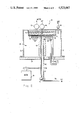
- FIG. 2 is a simplified cross-sectional view of a novel apparatus useful in practicing the novel process of the present invention
- FIG. 3 is a partial enlarged view of the apparatus of FIG. 2, depicting the treatment of one partially cross-sectioned wafer;
- FIGS. 4 to 7 are simplified sequential cross-sectional views of the migration of one droplet through a wafer in the process of the present invention.
- FIG. 8 is an enlarged simplified cross-sectional view of FIG. 3, with a buffer layer provided between the wafer bottom surface and the heating surface.
- a three-dimensional microelectronic device 12 which comprises a plurality of stacked semiconductor wafers 14. As an example, three of such wafers 14 are shown. Each wafer 14 is connected to another wafer 14 by external leads 16 which may extend from either of surfaces 18, 20 of wafer 14, thereby allowing the transfer of signals from one wafer 14 to another.
- the transfer of signals through wafer 14 is provided by internal connections 22 which are positioned between wafer surfaces 18, 20. The process for fabricating such internal connections 22 is the subject of the present invention.
- the process of the present invention employs a technique generally referred to as thermal gradient zone melting.
- a wafer 14 of suitable semiconductor material which is of one type of conductivity, is selected.
- a wafer 14 of n-type silicon is selected.
- Wafer 14 has a top surface 18 and a bottom surface 20.
- Solid droplets 24, a suitable metal-rich conductive material of an opposite type of conductivity, are placed on wafer top surface 18, as best shown by a representative single droplet 24 in FIG. 5.
- droplets 24 of aluminum are selected.
- droplets are generally referred to as droplets irrespective of either solid or liquid form.
- droplets 24 may be deposited in a predetermined pattern, as depicted by FIG. 1.
- Wafer 14 is then heated to an elevated temperature in order to establish a thermal gradient through wafer 14, with bottom surface 20 being the hotter surface.
- aluminum droplet 24 is heated to form a liquid which is generally referred to as a liquid zone.
- droplet 24 then migrates through wafer 14 toward hotter surface 20. As it migrates, droplet 24 leaves a recrystallized path which is of an opposite conductivity than the conductivity of wafer 14.
- the column-like path, p-type silicon in the example eventually becomes conductive connection 22.
- Apparatus 30 comprises removable chamber wall 32 and chamber base 34 which combine to form thermomigration chamber 36.
- apparatus 30 further comprises rotatable heating platform 40 which includes a generally planar heating surface 42 for supporting at least one wafer 14, two of which are shown as an example in FIG. 2.
- heating surface 42 is adapted to receive the entire area of wafer bottom surface 20.
- Platform 40 generally comprises a heat conductive material, for example, graphite.
- Radio-frequency coils 44 are positioned beneath heating platform 40 to induce heat therein in order to heat wafers 14.
- a heat sink 46 which is spaced from heating surface 42, is provided for wafers 14.
- heat sink 46 is a water tank.
- gap 48 between wafer top surface 18 and water tank 46, as best shown in FIG. 3, is provided to receive a gas of high heat conductivity such as hydrogen or helium.
- the gas may be in either a pure or a mixed form.
- helium is selected. The cooperative action of water tank 46 and the gas removes heat from wafer 14 to enhance the establishment of the desired thermal gradient through wafer 14.
- apparatus 30 comprises radio-frequency conductors 50 which, exiting through chamber base 34, are connected to a radio frequency source, not shown.
- Heating platform 40 is mounted on rotatable platform drive shaft 60.
- Motor 64 which is connected to elevatable drive shaft 62 which in turn is connected to platform drive shaft 60, is adapted to rotate platform 40.
- Gas conduit 57 connected to gas entry port 56 at its external end 61, is provided within platform drive shaft 60 and drive shaft 62. Internal end 63 of gas conduit 57 is positioned adjacent heating platform 40.
- water entry and exit ports 52, 54, and gas entry and exit ports 56, 58 are provided.
- a wafer 14 of one type of conductivity for example, n-type silicon
- Wafer 14 has two major parallel opposed top and bottom surfaces 18, 20, as best shown in FIG. 3.
- Wafer 14 of the preferred embodiment has a thickness, designated as d W , of typically 20 mils.
- an array of solid droplets 24 of suitable metal-rich conductive material is placed on top surface 18 of wafer 14, as best shown by the representative single droplet 24 in FIG. 5.
- Droplets 24 are of an opposite conductivity, for example, aluminum.
- This array arranged in a typical 32 ⁇ 32 matrix as similar to what is shown in FIG. 1, is applied to surface 18 by conventional techniques such as direct evaporation using a shadow mask.
- Each droplet 24 in the preferred embodiment for example, is approximately 3 mils in diameter and 8 to 25 micrometers in height, with a droplet center-to-droplet center distance of approximately 20 mils.
- two wafers 14, as an example are placed directly on graphite heating platform 40, with the entire area of wafer bottom surface 20 in direct physical contact with heating surface 42, as best shown by the single wafer 14 in FIG. 3.
- RF coils 44 then induce eddy currents in graphite platform 40 which, being resistive in property, transforms electrical energy into heat.
- Coils 44 receive RF energy through conductors 50 which in turn are connected to a RF source, not shown.
- the heat conductive gas enters chamber 36 through entry port 56 and water enters water tank 46 through entry port 52.
- Gap 48, d G which is approximately 5 mils in distance in the example, is provided to receive the gas.
- water of room temperature in tank 46, exiting through port 54 conveniently circulates at a rate of approximately 5-6 gallons per minute for cooling the heat conductive gas.
- the gas in chamber 36, exiting through port 58 conveniently circulates at a rate of approximately 10 cubic feet per minute for transporting the heat from wafer 14 to water tank 46.
- droplets 24 are heated to a liquid state.
- liquid aluminum droplets 24 migrate uniformally toward heating surface 42, as partially shown in FIG. 3.
- paths 22 are p-type silicon which contain traces of aluminum.
- each of the resultant internal connections 22 has a resistance of approximately 5 to 15 ohms.
- a buffer layer 70 is applied to the entire area of bottom surface 20, interposing between bottom surface 20 and heating surface 42.
- Buffer layer 70 has the characteristic of being insoluble with liquid droplets 24. This enables buffer layer 70 to trap and terminate the migration of droplets 24, thereby preventing alloying or sticking of droplets 24 with heating surface 42. Buffer layer 70, thus, facilitates the subsequent removal of wafer 14 from heating surface 42.
- Buffer layer 70 comprises a material such as silicon dioxide or aluminum oxide. The process employing buffer layer 70 is described and claimed in the above-mentioned copending application by Kuen Chow and Jan Grinberg.
- Buffer layer 70 which is silicon dioxide of conventional purity in the example, is applied to wafer bottom surface 20 by conventional techniques such as vapor deposition. Buffer layer 70, for example, is approximately one micrometer in thickness. After removal from heating surface 42, buffer layer 70 is removed by conventional resurfacing techniques such as grinding and polishing.
- a thermal gradient of 250° C./cm is established through wafer 14 in accordance with the invention.
- the resultant thermal gradient is approximately 2 to 5 times larger than the gradients disclosed in the prior art.
- the comparatively high thermal gradient allows the migration of droplets 24 to be completed in approximately 10 minutes. With wafers 14 being exposed to chamber heat for only such a comparatively short duration, more defect-free wafers are manufactured. Moreover, such a comparatively high thermal gradient enhances uniform migration of droplets 24, which in turn produces more wafers with completed migrations.
- the distance of gap 48, d G may be narrowed. Because the thermal gradient generally corresponds inversely to the distance of gap 48, a narrowing of distance d g to 2 mils increases the thermal gradient across wafer 14. This is due to the fact that water tank 46 is now closer to wafer 14 and is able to provide more heat removing capability.
- the narrowing of d G is accomplished by elevating drive shaft 62, which in turn elevates platform 40 and wafer 14 supported thereon.
- the narrowing of d G allows the process to proceed at either an even faster migration rate or a lower temperature.
- the lower temperature process permits migrations in a lower thermal gradient. Either selection results in even more defect-free wafers.
Landscapes
- Engineering & Computer Science (AREA)
- Chemical & Material Sciences (AREA)
- Physics & Mathematics (AREA)
- Materials Engineering (AREA)
- Metallurgy (AREA)
- Organic Chemistry (AREA)
- Crystallography & Structural Chemistry (AREA)
- Condensed Matter Physics & Semiconductors (AREA)
- General Physics & Mathematics (AREA)
- Manufacturing & Machinery (AREA)
- Computer Hardware Design (AREA)
- Microelectronics & Electronic Packaging (AREA)
- Power Engineering (AREA)
- Cooling Or The Like Of Semiconductors Or Solid State Devices (AREA)
Abstract
Description
Claims (6)
Priority Applications (4)
| Application Number | Priority Date | Filing Date | Title |
|---|---|---|---|
| US06/366,901 US4523067A (en) | 1982-04-09 | 1982-04-09 | Temperature gradient zone melting apparatus |
| PCT/US1983/000478 WO1983003710A1 (en) | 1982-04-09 | 1983-04-06 | Temperature gradient zone melting process and apparatus |
| EP83901544A EP0105347B1 (en) | 1982-04-09 | 1983-04-06 | Temperature gradient zone melting process and apparatus |
| DE8383901544T DE3369599D1 (en) | 1982-04-09 | 1983-04-06 | Temperature gradient zone melting process and apparatus |
Applications Claiming Priority (1)
| Application Number | Priority Date | Filing Date | Title |
|---|---|---|---|
| US06/366,901 US4523067A (en) | 1982-04-09 | 1982-04-09 | Temperature gradient zone melting apparatus |
Publications (1)
| Publication Number | Publication Date |
|---|---|
| US4523067A true US4523067A (en) | 1985-06-11 |
Family
ID=23445069
Family Applications (1)
| Application Number | Title | Priority Date | Filing Date |
|---|---|---|---|
| US06/366,901 Expired - Lifetime US4523067A (en) | 1982-04-09 | 1982-04-09 | Temperature gradient zone melting apparatus |
Country Status (1)
| Country | Link |
|---|---|
| US (1) | US4523067A (en) |
Cited By (2)
| Publication number | Priority date | Publication date | Assignee | Title |
|---|---|---|---|---|
| US5218178A (en) * | 1991-07-01 | 1993-06-08 | Inductotherm Corp. | Method of and apparatus for internal heating of solid bodies using electromagnetic induction |
| US5554836A (en) * | 1994-05-23 | 1996-09-10 | The Boc Group, Inc. | Induction heating in low oxygen-containing atmosphere |
Citations (6)
| Publication number | Priority date | Publication date | Assignee | Title |
|---|---|---|---|---|
| US3521018A (en) * | 1968-09-26 | 1970-07-21 | Ibm | Temperature sensor |
| US3845738A (en) * | 1973-09-12 | 1974-11-05 | Rca Corp | Vapor deposition apparatus with pyrolytic graphite heat shield |
| US3895967A (en) * | 1973-10-30 | 1975-07-22 | Gen Electric | Semiconductor device production |
| US3897277A (en) * | 1973-10-30 | 1975-07-29 | Gen Electric | High aspect ratio P-N junctions by the thermal gradient zone melting technique |
| US4001047A (en) * | 1975-05-19 | 1977-01-04 | General Electric Company | Temperature gradient zone melting utilizing infrared radiation |
| US4035199A (en) * | 1976-08-30 | 1977-07-12 | General Electric Company | Process for thermal gradient zone melting utilizing a guard ring radiation coating |
-
1982
- 1982-04-09 US US06/366,901 patent/US4523067A/en not_active Expired - Lifetime
Patent Citations (6)
| Publication number | Priority date | Publication date | Assignee | Title |
|---|---|---|---|---|
| US3521018A (en) * | 1968-09-26 | 1970-07-21 | Ibm | Temperature sensor |
| US3845738A (en) * | 1973-09-12 | 1974-11-05 | Rca Corp | Vapor deposition apparatus with pyrolytic graphite heat shield |
| US3895967A (en) * | 1973-10-30 | 1975-07-22 | Gen Electric | Semiconductor device production |
| US3897277A (en) * | 1973-10-30 | 1975-07-29 | Gen Electric | High aspect ratio P-N junctions by the thermal gradient zone melting technique |
| US4001047A (en) * | 1975-05-19 | 1977-01-04 | General Electric Company | Temperature gradient zone melting utilizing infrared radiation |
| US4035199A (en) * | 1976-08-30 | 1977-07-12 | General Electric Company | Process for thermal gradient zone melting utilizing a guard ring radiation coating |
Cited By (2)
| Publication number | Priority date | Publication date | Assignee | Title |
|---|---|---|---|---|
| US5218178A (en) * | 1991-07-01 | 1993-06-08 | Inductotherm Corp. | Method of and apparatus for internal heating of solid bodies using electromagnetic induction |
| US5554836A (en) * | 1994-05-23 | 1996-09-10 | The Boc Group, Inc. | Induction heating in low oxygen-containing atmosphere |
Similar Documents
| Publication | Publication Date | Title |
|---|---|---|
| EP0423327B1 (en) | Apparatus and method for treating flat substrates under reduced pressure | |
| US6359264B1 (en) | Thermal cycling module | |
| JP4970679B2 (en) | Plasma reaction chamber component with improved temperature uniformity and processing method using the same | |
| KR100974130B1 (en) | Substrate support having brazed plates and heater | |
| US4041278A (en) | Heating apparatus for temperature gradient zone melting | |
| US3895967A (en) | Semiconductor device production | |
| KR20170038886A (en) | Wafer carrier with independent isolated heater zones | |
| CN1653591A (en) | Process and system for heating semiconductor substrates in a processing chamber containing a susceptor | |
| KR920701534A (en) | Semiconductor Wafer Processing Apparatus and Method | |
| US20060242967A1 (en) | Termoelectric heating and cooling apparatus for semiconductor processing | |
| US20050072525A1 (en) | Apparatus to improve wafer temperature uniformity for face-up wet processing | |
| JP2725026B2 (en) | Evaporation source for evaporation | |
| JP2018525808A (en) | Thermal management system and method for wafer processing systems | |
| EP0105347B1 (en) | Temperature gradient zone melting process and apparatus | |
| US4523067A (en) | Temperature gradient zone melting apparatus | |
| US4398974A (en) | Temperature gradient zone melting process employing a buffer layer | |
| US3397448A (en) | Semiconductor integrated circuits and method of making same | |
| US3977955A (en) | Method for cathodic sputtering including suppressing temperature rise | |
| CN100472706C (en) | Integrally formed bake plate unit for use in wafer fabrication system | |
| US4091257A (en) | Deep diode devices and method and apparatus | |
| US2900584A (en) | Transistor method and product | |
| US3764511A (en) | Moated substrate holding pedestal | |
| JPS59500643A (en) | Temperature gradient zone melting process and equipment | |
| KR100348439B1 (en) | Method and device for producing electrically conductive continuity in semiconductor components | |
| JPH0778796A (en) | Method and equipment for manufacturing semiconductor device |
Legal Events
| Date | Code | Title | Description |
|---|---|---|---|
| AS | Assignment |
Owner name: HUGHES AIRCRAFT COMPANY CULVER CITY CA A CORP OF D Free format text: ASSIGNMENT OF ASSIGNORS INTEREST.;ASSIGNORS:BROWN, ROGER H.;CHOW, KUEN;GOODWIN, NORMAN W.;AND OTHERS;REEL/FRAME:004002/0848 Effective date: 19820402 Owner name: HUGHES AIRCRAFT COMPANY, A CORP OF DE, CALIFORNIA Free format text: ASSIGNMENT OF ASSIGNORS INTEREST;ASSIGNORS:BROWN, ROGER H.;CHOW, KUEN;GOODWIN, NORMAN W.;AND OTHERS;REEL/FRAME:004002/0848 Effective date: 19820402 |
|
| STCF | Information on status: patent grant |
Free format text: PATENTED CASE |
|
| FPAY | Fee payment |
Year of fee payment: 4 |
|
| SULP | Surcharge for late payment | ||
| FPAY | Fee payment |
Year of fee payment: 8 |
|
| SULP | Surcharge for late payment | ||
| REMI | Maintenance fee reminder mailed | ||
| FPAY | Fee payment |
Year of fee payment: 12 |
|
| SULP | Surcharge for late payment | ||
| AS | Assignment |
Owner name: HUGHES ELECTRONICS CORPORATION, CALIFORNIA Free format text: ASSIGNMENT OF ASSIGNORS INTEREST;ASSIGNOR:HE HOLDINGS INC., HUGHES ELECTRONICS FORMERLY KNOWN AS HUGHES AIRCRAFT COMPANY;REEL/FRAME:009350/0366 Effective date: 19971217 |