US4445736A - Method and apparatus for producing a premolded packaging - Google Patents
Method and apparatus for producing a premolded packaging Download PDFInfo
- Publication number
- US4445736A US4445736A US06/364,165 US36416582A US4445736A US 4445736 A US4445736 A US 4445736A US 36416582 A US36416582 A US 36416582A US 4445736 A US4445736 A US 4445736A
- Authority
- US
- United States
- Prior art keywords
- terminals
- package
- web
- forming
- portions
- Prior art date
- Legal status (The legal status is an assumption and is not a legal conclusion. Google has not performed a legal analysis and makes no representation as to the accuracy of the status listed.)
- Expired - Fee Related
Links
Images


Classifications
-
- H—ELECTRICITY
- H05—ELECTRIC TECHNIQUES NOT OTHERWISE PROVIDED FOR
- H05K—PRINTED CIRCUITS; CASINGS OR CONSTRUCTIONAL DETAILS OF ELECTRIC APPARATUS; MANUFACTURE OF ASSEMBLAGES OF ELECTRICAL COMPONENTS
- H05K7/00—Constructional details common to different types of electric apparatus
- H05K7/02—Arrangements of circuit components or wiring on supporting structure
- H05K7/10—Plug-in assemblages of components, e.g. IC sockets
- H05K7/1053—Plug-in assemblages of components, e.g. IC sockets having interior leads
- H05K7/1076—Plug-in assemblages of components, e.g. IC sockets having interior leads co-operating by sliding
-
- Y—GENERAL TAGGING OF NEW TECHNOLOGICAL DEVELOPMENTS; GENERAL TAGGING OF CROSS-SECTIONAL TECHNOLOGIES SPANNING OVER SEVERAL SECTIONS OF THE IPC; TECHNICAL SUBJECTS COVERED BY FORMER USPC CROSS-REFERENCE ART COLLECTIONS [XRACs] AND DIGESTS
- Y10—TECHNICAL SUBJECTS COVERED BY FORMER USPC
- Y10T—TECHNICAL SUBJECTS COVERED BY FORMER US CLASSIFICATION
- Y10T29/00—Metal working
- Y10T29/49—Method of mechanical manufacture
- Y10T29/49002—Electrical device making
- Y10T29/49117—Conductor or circuit manufacturing
- Y10T29/49121—Beam lead frame or beam lead device
-
- Y—GENERAL TAGGING OF NEW TECHNOLOGICAL DEVELOPMENTS; GENERAL TAGGING OF CROSS-SECTIONAL TECHNOLOGIES SPANNING OVER SEVERAL SECTIONS OF THE IPC; TECHNICAL SUBJECTS COVERED BY FORMER USPC CROSS-REFERENCE ART COLLECTIONS [XRACs] AND DIGESTS
- Y10—TECHNICAL SUBJECTS COVERED BY FORMER USPC
- Y10T—TECHNICAL SUBJECTS COVERED BY FORMER US CLASSIFICATION
- Y10T29/00—Metal working
- Y10T29/49—Method of mechanical manufacture
- Y10T29/49002—Electrical device making
- Y10T29/49117—Conductor or circuit manufacturing
- Y10T29/49204—Contact or terminal manufacturing
- Y10T29/49208—Contact or terminal manufacturing by assembling plural parts
- Y10T29/4922—Contact or terminal manufacturing by assembling plural parts with molding of insulation
Definitions
- the present invention relates to a method and apparatus for the formation of premolded packages to receive integrated circuit chips therein, also known as leadless substrates, and in particular to a method and apparatus which overcomes many of the difficulties of the prior art.
- the present invention overcomes many of the difficulties of the noted prior art by providing a multi-step process for forming the subject package.
- the present invention includes the step of stamping and forming first and second webs of conductive material to form arrays of parallel spaced terminals. Each web can then be selectively plated, as desired, with material of the desired type and thickness at the proper locations.
- One of the webs is then subjected to a first molding operation in which first portions of the packaged frame are molded to opposite ends of the terminals.
- the thus formed partial package is then subjected to a cutting and forming operation which separates intermediate their ends and forms the terminals about the partial package.
- the second web of terminals is placed in an overlying position between the partial package extending transversely to the first web and in contact therewith.
- the partial package is next passed through a second molding operation which forms second portions of the package at opposite ends of the terminals of the second web while integrally joining the first package portions.
- the thus formed package is then passed to a second cutting and forming operation which forms the second terminals with respect to the package and separates the package from the carrier webs.
- the thus formed package can then be inspected, packaged, and shipped.
- FIG. 1 is a schematic diagram of the steps of the present invention
- FIG. 2 is a schematic diagram of the stamping and plating operations forming each of the conductive webs utilized in the present invention
- FIG. 3 is a schematic diagram of the first molding station and first forming station of the present invention.
- FIG. 4 is a schematic diagram of the second molding station
- FIGS. 5 to 7 are transverse sections through a portion of the subject package showing the steps in forming a representative terminal
- FIG. 8 is a perspective view of the first web according to the present invention with the first portion of the housing molded thereon;
- FIG. 9 is a perspective view of the partial package as it would appear at the station with the second web overlying the first and ready for the second molding operation;
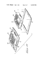
- FIG. 10 is a perspective view of the fully molded package according to the present invention as it is separated from the carrier webs;
- FIG. 11 is a perspective view of a package according to the present invention.
- FIG. 12 is a top plan view of the package according to the subject invention.
- FIG. 13 is a side elevation of the package according to the present invention.
- FIG. 14 is a transverse section through one wall of the package showing a typical terminal configuration.
- the subject invention is shown in an overall block level schematic in FIG. 1.
- the subject invention starts with a pair of continuous webs of conductive material, each of which passes through a stamping operation 10 to form a ladder-like array of a plurality of spaced apart terminals 14 extending transversely across the web 12 and joined at both ends by the continuous carrier portion 16, 18.
- Each of the thus formed webs can then pass to a selective plating operation 20 where plating 22, of the desired type and thickness, is applied to the terminals at the desired location.
- plating 22 of the desired type and thickness
- the thus formed partial package moves to the next station 30 where the terminals are cut substantially centrally of their ends and formed about the housing as shown in FIGS. 5 through 7.
- the partial package is now in the condition shown in FIGS. 3 and 9.
- the second web is brought into overlying transverse relationship, as shown in FIG. 9.
- the partial package is then moved to full molding station 30, as shown in FIG. 4, where second housing portions 34, 36 are molded on the second terminals with the ends of the second housing portions integrally joining the first housing portions 26, 28.
- the package goes to a second cut and forming station 38 where the second terminals are cut substantially centrally of their ends and formed, as previously described.
- the completed package is separated from the carrier webs.
- the completed package can now be passed to an optical inspection station 40 and to a final packaging station 42 where they will be readied for shipment.
Landscapes
- Engineering & Computer Science (AREA)
- Microelectronics & Electronic Packaging (AREA)
- Manufacturing Of Electrical Connectors (AREA)
Abstract
Description
Claims (4)
Priority Applications (1)
| Application Number | Priority Date | Filing Date | Title |
|---|---|---|---|
| US06/364,165 US4445736A (en) | 1982-03-31 | 1982-03-31 | Method and apparatus for producing a premolded packaging |
Applications Claiming Priority (1)
| Application Number | Priority Date | Filing Date | Title |
|---|---|---|---|
| US06/364,165 US4445736A (en) | 1982-03-31 | 1982-03-31 | Method and apparatus for producing a premolded packaging |
Publications (1)
| Publication Number | Publication Date |
|---|---|
| US4445736A true US4445736A (en) | 1984-05-01 |
Family
ID=23433332
Family Applications (1)
| Application Number | Title | Priority Date | Filing Date |
|---|---|---|---|
| US06/364,165 Expired - Fee Related US4445736A (en) | 1982-03-31 | 1982-03-31 | Method and apparatus for producing a premolded packaging |
Country Status (1)
| Country | Link |
|---|---|
| US (1) | US4445736A (en) |
Cited By (23)
| Publication number | Priority date | Publication date | Assignee | Title |
|---|---|---|---|---|
| US4504887A (en) * | 1983-04-01 | 1985-03-12 | Amp Incorporated | Leadless integrated circuit package housing having means for contact replacement |
| US4547964A (en) * | 1982-08-09 | 1985-10-22 | Sony Corporation | Method for the manufacture of a printed-circuit board connector |
| US4628597A (en) * | 1983-11-25 | 1986-12-16 | Meehan Robert F | Method of making an electrical connector |
| US4712721A (en) * | 1986-03-17 | 1987-12-15 | Raychem Corp. | Solder delivery systems |
| US4761875A (en) * | 1986-04-17 | 1988-08-09 | Fuji Photo Film Co., Ltd. | Method of manufacturing pad for magnetic recording tape cassette |
| US4785532A (en) * | 1985-10-22 | 1988-11-22 | Amp Incorporated | Method of making electrical connector assembly for antiskid braking system |
| US5012391A (en) * | 1989-08-17 | 1991-04-30 | Amp Incorporated | Molded electrical interconnection system |
| US5062802A (en) * | 1990-11-01 | 1991-11-05 | Amp Incorporated | Contact module for a low height multi-chip carrier socket |
| US5074039A (en) * | 1990-10-26 | 1991-12-24 | Amp Incorporated | Method of manufacturing electrical connectors |
| US5201883A (en) * | 1991-08-30 | 1993-04-13 | Kel Corporation | Method of making in-molded plug connector |
| US5339518A (en) * | 1993-07-06 | 1994-08-23 | Motorola, Inc. | Method for making a quad leadframe for a semiconductor device |
| US5722861A (en) * | 1996-02-28 | 1998-03-03 | Molex Incorporated | Electrical connector with terminals of varying lengths |
| US5768777A (en) * | 1994-04-08 | 1998-06-23 | Berg Technology Inc. | Method of making low profile connector |
| US5822855A (en) * | 1995-04-26 | 1998-10-20 | The Whitaker Corporation | Method of making electrical connector having a two part articulated housing |
| US5879610A (en) * | 1991-03-21 | 1999-03-09 | The Whitaker Corporation | Method of making an electrical connector |
| US6247227B1 (en) * | 1996-08-02 | 2001-06-19 | Dial Tool Industries | Apparatus for assembling parts in a carrier strip |
| US20020076990A1 (en) * | 2000-12-15 | 2002-06-20 | Sumitomo Wiring Systems Ltd. | Apparatus for processing a stacked-type connector of a wire harness, a housing holder, apparatus and method and for stacking housings of a stacked-type connectors, and apparatus for pressing a joint portion of stacked-type connector |
| US6645013B1 (en) * | 1999-07-05 | 2003-11-11 | Molex Japan Co. Ltd. | Electronic system and connector used therein |
| US6665932B2 (en) * | 2001-05-21 | 2003-12-23 | Nagano Fujitsu Component | SMT connector and method of production of same |
| US20070082513A1 (en) * | 2005-09-29 | 2007-04-12 | Tieyu Zheng | Self-balanced dual L-shaped socket |
| EP1876004A1 (en) * | 2006-07-06 | 2008-01-09 | Stanzbiegetechnik Ges.M.B.H. | Method for producing injection overmoulded parts |
| US20080014785A1 (en) * | 2004-03-01 | 2008-01-17 | Matsushita Electric Works, Ltd. | Connector assembly |
| US20170110270A1 (en) * | 2014-03-19 | 2017-04-20 | Panasonic Intellectual Property Management Co., Ltd. | Electronic component |
Citations (13)
| Publication number | Priority date | Publication date | Assignee | Title |
|---|---|---|---|---|
| US3287795A (en) * | 1964-06-05 | 1966-11-29 | Western Electric Co | Methods of assembling electrical components with circuits |
| FR1528075A (en) * | 1967-04-28 | 1968-06-07 | Radiotechnique Coprim Rtc | Housing for a semiconductor device and its manufacturing process |
| US3389461A (en) * | 1965-04-08 | 1968-06-25 | Ibm | Molded insulator base having embedded terminals and method of forming the same |
| US3574929A (en) * | 1969-06-02 | 1971-04-13 | Bourns Inc | Adustable resistors and method |
| US3693239A (en) * | 1969-07-25 | 1972-09-26 | Sidney Dix | A method of making a micromodular package |
| US3798763A (en) * | 1972-03-24 | 1974-03-26 | M Deltoer | Method of making a rotary switch stator |
| US4079511A (en) * | 1976-07-30 | 1978-03-21 | Amp Incorporated | Method for packaging hermetically sealed integrated circuit chips on lead frames |
| US4142287A (en) * | 1976-12-27 | 1979-03-06 | Amp Incorporated | Electrical devices such as watches and method of construction thereof |
| US4195193A (en) * | 1979-02-23 | 1980-03-25 | Amp Incorporated | Lead frame and chip carrier housing |
| US4197636A (en) * | 1976-06-01 | 1980-04-15 | Olympus Optical Co., Ltd. | Method of producing a structure of connection terminals |
| US4225209A (en) * | 1979-05-18 | 1980-09-30 | Amp Incorporated | Electrical connector receptacle |
| US4337574A (en) * | 1978-12-14 | 1982-07-06 | Amp Incorporated | Method of manufacturing electrical connector receptacles |
| US4395084A (en) * | 1981-07-06 | 1983-07-26 | Teledyne Industries, Inc. | Electrical socket for leadless integrated circuit packages |
-
1982
- 1982-03-31 US US06/364,165 patent/US4445736A/en not_active Expired - Fee Related
Patent Citations (13)
| Publication number | Priority date | Publication date | Assignee | Title |
|---|---|---|---|---|
| US3287795A (en) * | 1964-06-05 | 1966-11-29 | Western Electric Co | Methods of assembling electrical components with circuits |
| US3389461A (en) * | 1965-04-08 | 1968-06-25 | Ibm | Molded insulator base having embedded terminals and method of forming the same |
| FR1528075A (en) * | 1967-04-28 | 1968-06-07 | Radiotechnique Coprim Rtc | Housing for a semiconductor device and its manufacturing process |
| US3574929A (en) * | 1969-06-02 | 1971-04-13 | Bourns Inc | Adustable resistors and method |
| US3693239A (en) * | 1969-07-25 | 1972-09-26 | Sidney Dix | A method of making a micromodular package |
| US3798763A (en) * | 1972-03-24 | 1974-03-26 | M Deltoer | Method of making a rotary switch stator |
| US4197636A (en) * | 1976-06-01 | 1980-04-15 | Olympus Optical Co., Ltd. | Method of producing a structure of connection terminals |
| US4079511A (en) * | 1976-07-30 | 1978-03-21 | Amp Incorporated | Method for packaging hermetically sealed integrated circuit chips on lead frames |
| US4142287A (en) * | 1976-12-27 | 1979-03-06 | Amp Incorporated | Electrical devices such as watches and method of construction thereof |
| US4337574A (en) * | 1978-12-14 | 1982-07-06 | Amp Incorporated | Method of manufacturing electrical connector receptacles |
| US4195193A (en) * | 1979-02-23 | 1980-03-25 | Amp Incorporated | Lead frame and chip carrier housing |
| US4225209A (en) * | 1979-05-18 | 1980-09-30 | Amp Incorporated | Electrical connector receptacle |
| US4395084A (en) * | 1981-07-06 | 1983-07-26 | Teledyne Industries, Inc. | Electrical socket for leadless integrated circuit packages |
Cited By (26)
| Publication number | Priority date | Publication date | Assignee | Title |
|---|---|---|---|---|
| US4547964A (en) * | 1982-08-09 | 1985-10-22 | Sony Corporation | Method for the manufacture of a printed-circuit board connector |
| US4504887A (en) * | 1983-04-01 | 1985-03-12 | Amp Incorporated | Leadless integrated circuit package housing having means for contact replacement |
| US4628597A (en) * | 1983-11-25 | 1986-12-16 | Meehan Robert F | Method of making an electrical connector |
| US4785532A (en) * | 1985-10-22 | 1988-11-22 | Amp Incorporated | Method of making electrical connector assembly for antiskid braking system |
| US4712721A (en) * | 1986-03-17 | 1987-12-15 | Raychem Corp. | Solder delivery systems |
| US4761875A (en) * | 1986-04-17 | 1988-08-09 | Fuji Photo Film Co., Ltd. | Method of manufacturing pad for magnetic recording tape cassette |
| US5012391A (en) * | 1989-08-17 | 1991-04-30 | Amp Incorporated | Molded electrical interconnection system |
| US5074039A (en) * | 1990-10-26 | 1991-12-24 | Amp Incorporated | Method of manufacturing electrical connectors |
| US5062802A (en) * | 1990-11-01 | 1991-11-05 | Amp Incorporated | Contact module for a low height multi-chip carrier socket |
| US5879610A (en) * | 1991-03-21 | 1999-03-09 | The Whitaker Corporation | Method of making an electrical connector |
| US5201883A (en) * | 1991-08-30 | 1993-04-13 | Kel Corporation | Method of making in-molded plug connector |
| US5339518A (en) * | 1993-07-06 | 1994-08-23 | Motorola, Inc. | Method for making a quad leadframe for a semiconductor device |
| US5768777A (en) * | 1994-04-08 | 1998-06-23 | Berg Technology Inc. | Method of making low profile connector |
| US5822855A (en) * | 1995-04-26 | 1998-10-20 | The Whitaker Corporation | Method of making electrical connector having a two part articulated housing |
| US5722861A (en) * | 1996-02-28 | 1998-03-03 | Molex Incorporated | Electrical connector with terminals of varying lengths |
| US6247227B1 (en) * | 1996-08-02 | 2001-06-19 | Dial Tool Industries | Apparatus for assembling parts in a carrier strip |
| US6645013B1 (en) * | 1999-07-05 | 2003-11-11 | Molex Japan Co. Ltd. | Electronic system and connector used therein |
| US20020076990A1 (en) * | 2000-12-15 | 2002-06-20 | Sumitomo Wiring Systems Ltd. | Apparatus for processing a stacked-type connector of a wire harness, a housing holder, apparatus and method and for stacking housings of a stacked-type connectors, and apparatus for pressing a joint portion of stacked-type connector |
| EP1220366A3 (en) * | 2000-12-25 | 2004-01-07 | Sumitomo Wiring Systems, Ltd. | Apparatus and method for processing a stacked-type connector of a wire harness |
| US6665932B2 (en) * | 2001-05-21 | 2003-12-23 | Nagano Fujitsu Component | SMT connector and method of production of same |
| US20080014785A1 (en) * | 2004-03-01 | 2008-01-17 | Matsushita Electric Works, Ltd. | Connector assembly |
| US7430801B2 (en) * | 2004-03-01 | 2008-10-07 | Matsushita Electric Works, Ltd. | Connector assembly |
| US20070082513A1 (en) * | 2005-09-29 | 2007-04-12 | Tieyu Zheng | Self-balanced dual L-shaped socket |
| US7419383B2 (en) * | 2005-09-29 | 2008-09-02 | Intel Corporation | Self-balanced dual L-shaped socket |
| EP1876004A1 (en) * | 2006-07-06 | 2008-01-09 | Stanzbiegetechnik Ges.M.B.H. | Method for producing injection overmoulded parts |
| US20170110270A1 (en) * | 2014-03-19 | 2017-04-20 | Panasonic Intellectual Property Management Co., Ltd. | Electronic component |
Similar Documents
| Publication | Publication Date | Title |
|---|---|---|
| US4445736A (en) | Method and apparatus for producing a premolded packaging | |
| US5070039A (en) | Method of making an integrated circuit using a pre-served dam bar to reduce mold flash and to facilitate flash removal | |
| EP0015111B1 (en) | Lead frame and housing for integrated circuit | |
| US3611061A (en) | Multiple lead integrated circuit device and frame member for the fabrication thereof | |
| US3650648A (en) | System for molding electronic components | |
| US5321305A (en) | LED manufacturing frame and method of using the same for manufacturing LEDs | |
| EP0971401B1 (en) | Method of manufacturing semiconductor devices and a resin molding machine therefor | |
| US3781976A (en) | Method of manufacturing chip-shaped solid state electrolytic capacitors | |
| US4951119A (en) | Lead frame for semiconductor devices | |
| US4137628A (en) | Method of manufacturing connection-type ceramic packages for integrated circuits | |
| US4874086A (en) | Film carrier and a method for manufacturing a semiconductor device utilizing the same | |
| US20030024105A1 (en) | Process for manufacturing fuse devices | |
| EP0806063A1 (en) | Array of electrical components with leads attached | |
| US5239745A (en) | Method for the manufacture of finished self-stabilizing resistors | |
| US4733014A (en) | Lead frame | |
| US4628597A (en) | Method of making an electrical connector | |
| US3739438A (en) | System for molding electronic components | |
| US5920113A (en) | Leadframe structure having moveable sub-frame | |
| US3961413A (en) | Method and apparatus for the assembly of semiconductor devices | |
| US3978516A (en) | Lead frame assembly for a packaged semiconductor microcircuit | |
| US5317189A (en) | Axial lead frame | |
| US5251679A (en) | Apparatus for shaping outboard terminals of surface-mountable circuit modules | |
| KR960002494B1 (en) | Matrix Lead Frames for Manufacturing Multiple IC Packages | |
| US5391392A (en) | Method for manufacturing electrical components | |
| US5484097A (en) | Fabrication of hybrid semiconductor devices |
Legal Events
| Date | Code | Title | Description |
|---|---|---|---|
| AS | Assignment |
Owner name: AMP INCORPORATED, P.O. BOX 3608, HARRISBURG, PA Free format text: ASSIGNMENT OF ASSIGNORS INTEREST.;ASSIGNOR:HOPKINS, JOHN R.;REEL/FRAME:003983/0849 Effective date: 19820325 |
|
| FEPP | Fee payment procedure |
Free format text: PAYOR NUMBER ASSIGNED (ORIGINAL EVENT CODE: ASPN); ENTITY STATUS OF PATENT OWNER: LARGE ENTITY |
|
| FPAY | Fee payment |
Year of fee payment: 4 |
|
| REFU | Refund |
Free format text: REFUND OF EXCESS PAYMENTS PROCESSED (ORIGINAL EVENT CODE: R169); ENTITY STATUS OF PATENT OWNER: LARGE ENTITY |
|
| REMI | Maintenance fee reminder mailed | ||
| LAPS | Lapse for failure to pay maintenance fees | ||
| FP | Lapsed due to failure to pay maintenance fee |
Effective date: 19960501 |
|
| STCH | Information on status: patent discontinuation |
Free format text: PATENT EXPIRED DUE TO NONPAYMENT OF MAINTENANCE FEES UNDER 37 CFR 1.362 |