US4396683A - Photomask blank provided with a transparent electro-conductive layer - Google Patents
Photomask blank provided with a transparent electro-conductive layer Download PDFInfo
- Publication number
- US4396683A US4396683A US06/240,258 US24025881A US4396683A US 4396683 A US4396683 A US 4396683A US 24025881 A US24025881 A US 24025881A US 4396683 A US4396683 A US 4396683A
- Authority
- US
- United States
- Prior art keywords
- heavy metal
- photomask blank
- layer
- oxide
- transparent electroconductive
- Prior art date
- Legal status (The legal status is an assumption and is not a legal conclusion. Google has not performed a legal analysis and makes no representation as to the accuracy of the status listed.)
- Expired - Lifetime
Links
Images

Classifications
-
- G—PHYSICS
- G03—PHOTOGRAPHY; CINEMATOGRAPHY; ANALOGOUS TECHNIQUES USING WAVES OTHER THAN OPTICAL WAVES; ELECTROGRAPHY; HOLOGRAPHY
- G03F—PHOTOMECHANICAL PRODUCTION OF TEXTURED OR PATTERNED SURFACES, e.g. FOR PRINTING, FOR PROCESSING OF SEMICONDUCTOR DEVICES; MATERIALS THEREFOR; ORIGINALS THEREFOR; APPARATUS SPECIALLY ADAPTED THEREFOR
- G03F1/00—Originals for photomechanical production of textured or patterned surfaces, e.g., masks, photo-masks, reticles; Mask blanks or pellicles therefor; Containers specially adapted therefor; Preparation thereof
- G03F1/38—Masks having auxiliary features, e.g. special coatings or marks for alignment or testing; Preparation thereof
- G03F1/40—Electrostatic discharge [ESD] related features, e.g. antistatic coatings or a conductive metal layer around the periphery of the mask substrate
-
- G—PHYSICS
- G03—PHOTOGRAPHY; CINEMATOGRAPHY; ANALOGOUS TECHNIQUES USING WAVES OTHER THAN OPTICAL WAVES; ELECTROGRAPHY; HOLOGRAPHY
- G03F—PHOTOMECHANICAL PRODUCTION OF TEXTURED OR PATTERNED SURFACES, e.g. FOR PRINTING, FOR PROCESSING OF SEMICONDUCTOR DEVICES; MATERIALS THEREFOR; ORIGINALS THEREFOR; APPARATUS SPECIALLY ADAPTED THEREFOR
- G03F1/00—Originals for photomechanical production of textured or patterned surfaces, e.g., masks, photo-masks, reticles; Mask blanks or pellicles therefor; Containers specially adapted therefor; Preparation thereof
- G03F1/54—Absorbers, e.g. of opaque materials
-
- Y—GENERAL TAGGING OF NEW TECHNOLOGICAL DEVELOPMENTS; GENERAL TAGGING OF CROSS-SECTIONAL TECHNOLOGIES SPANNING OVER SEVERAL SECTIONS OF THE IPC; TECHNICAL SUBJECTS COVERED BY FORMER USPC CROSS-REFERENCE ART COLLECTIONS [XRACs] AND DIGESTS
- Y10—TECHNICAL SUBJECTS COVERED BY FORMER USPC
- Y10S—TECHNICAL SUBJECTS COVERED BY FORMER USPC CROSS-REFERENCE ART COLLECTIONS [XRACs] AND DIGESTS
- Y10S428/00—Stock material or miscellaneous articles
- Y10S428/913—Material designed to be responsive to temperature, light, moisture
Definitions
- This invention relates to an improvement of photomask blanks which are used in manufacturing semiconductor devices and the like.
- one of the most important steps is the step of forming any desired pattern by the use of photolithography.
- the miniaturization of such electronic circuits mainly depends on the accuracy achieved in this step.
- As the electronic circuits are 7eing miniaturized with higher density there is a change in the type of photomask, namely from the emulsion type photomask to the hard photomask.
- various pattern transfer techniques such as for ultraviolet light exposure, scale-down projection exposure, electronic beam exposure and others in addition to the conventional ultraviolet exposure process.
- the etching technique also is being changed from the prior art wet processing system to the dry processing system.
- the existing photomasks having patterns of a width in the scale of sub-micron are used even in manufacturing SLSI (super large scale integrated) circuits.
- the photomasks are thoroughly examined before they are used to manufacture semiconductive devices and the like because the photomask has its extremely important role.
- such examinations have been carried out by the use of a pattern examining machine which comprises an automated light microscope with higher precision. If the width in lines of the pattern is of one ⁇ m or less, however, such an optical system is incapable of examining them.
- a photomask checking system in which an electron beam is utilized instead of the optical system.
- An electroconductive photomask which includes a transparent and electroconductive layer coated on the photomask as a bottom layer for preventing the charge-up phenomenon, said layer being made of a material that will not be affected by an etchant of any light-screening material.
- This conductive photomask may be made of gold for improving the sensitivity to the electron beam, the gold being stronger against a reflected electron beam as a light-screening material.
- the gold photomask is not feasible because the gold has low physical strength.
- This invention relates to a practically useful photomask blank having improved properties with respect to the above-mentioned disadvantages of the prior art.
- the present invention more specifically relates to a photomask blank provided with a transparent electroconductive layer, comprising a base having (a) a transparent electroconductive material coated thereon, and also having (b) a heavy metal oxide layer laminated on said material (a) in direct contact therewith or through an intermediary light-screening layer of the same heavy metal as in said layer (b).
- a photomask blank is excellent in physical strength.
- the base used in this invention may be any material which is permeable to an electromagnetic wave to be used such as X-ray or laser ray.
- the transparent and electroconductive layer should also be transparent to such electromagnetic waves.
- the transparent and conductive layer can be formed of a material selected from the group consisting of indium oxide, tin oxide and lead oxide by, for example, vapor deposition such as vacuum evaporation or sputtering on the base under an oxygen atmosphere.
- the heavy metal in the present invention means those having a specific gravity of more than 10.0. More preferably, those metals having ⁇ 50% as much as the reflected electron beam intensity of gold, as measured by, for example, a conventional scanning type electron microscope, are useful.
- tungsten, tantalum and molybdenum are most preferred.
- this invention provides a photomask blank comprising a base covered by the coating of a transparent electroconductive material, a layer of a heavy metal disposed over said coating and a further oxide layer of the same heavy metal formed over said heavy metal layer for reducing the reflectance on the surface for an exposure light and for increasing the physical strength on the surface, said heavy metal being selected from the group consisting of tungsten, tantalum, molybdenum and such other materials that have a reflected electron beam intensity similar to that of gold.
- this invention provides a photomask blank comprising a base covered by the coating of a transparent electroconductive material and an oxide layer of said heavy metal formed over said coating, said heavy metal being oxidized to such an extent as to have no adverse effect on the reflected electron beam intensity and the light-screening of exposure light.
- each of the layers has a thickness generally in the range from 1 A to 1 ⁇ .
- the resultant conductive photomask can effectively be used in examining patterns by the use of an electron beam under practical speed and accuracy and is extremely practicable as a photomask for pattern transfer.
- the heavy metals such as tungsten, tantalum and molybdenum are conventionally used in the semiconductor industry and can easily be processed by plasma etching.
- FIG. 1 is a diagrammatic cross-section showing an embodiment of the photomask blank according to this invention
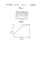
- FIG. 2 is the graph showing the relation between the thickness of a tungsten layer and the contrast of a reflected electron beam
- FIG. 3 is a graph showing the relationship between the thickness of the tungsten layer and the optical density.
- FIG. 4 is a graph showing the spectral reflectance on the surface in the photomask blank of this invention.
- the photomask blank comprises a base plate 1 of synthetic quartz, a layer 2 of a transparent electroconductive material, a light screening layer 3 of heavy metal such as tungsten or the like and an oxide layer 4 of the same heavy metal.
- FIG. 2 shows the relationship between the thickness of a tungsten layer and the contrast of a reflected electron beam. This contrast can be obtained by the use of the following formula.
- Contrast Intensity of electron reflected at the heavy metal layer/Intensity of electron reflected at the transparent electroconductive layer.
- FIG. 3 shows the relationship between the thickness of a tungsten layer and the optical density when a wavelength of the light used is 436 nm. It is understood from FIGS. 2 and 3 that the contrast in the electron beam and also the light-screening property (optical density) during exposure are sufficient in practice if the thickness of the tungsten layer is on the order of 1000 A.
- FIG. 4 illustrates the spectral reflectance at surface when the tungsten oxide layer at the top is 100 A or 200 A in thickness.
- the photomask blanks according to this invention can be easily patterned by using plasma etching of gaseous carbon tetrafluoride after a resist image has been formed by the conventional photolithography or electron-beam lithography.
- the photomask blank of this invention By using the photomask blank of this invention, electron-beam examination for lines in a pattern can be effectively carried out with higher accuracy and yet a practical photomask having less reflection at the pattern can be obtained. Therefore, this invention is extremely useful in manufacturing semiconductor circuits which require higher density in the patterns, particularly, SLSI circuits.
- Comparative sample an indium oxide layer was formed on a transparent base plate of glass which was placed within the sputtering device. Thereafter, a gold layer was vapor deposited over the transparent electroconductive layer in vacuo of 2 ⁇ 10 -5 Torr. This assembly is hereinafter referred to as Comparative sample.
- the photomask blank according to this invention is better suited for minute patterns because of its higher layer strength and lower surface reflectance, as compared with the prior art substrate having gold vapor deposited thereon.
Abstract
Description
______________________________________
           Sample No. 1
                    Comparative sample
______________________________________
Contrast of  3.5        3.3
reflected
electron
Film strength
             >500 g.    30 g.
Reflectance  <5%        35%
at surface
(436 nm)
Optical      2.8        1.7
transmission
density
______________________________________
Claims (15)
Applications Claiming Priority (2)
| Application Number | Priority Date | Filing Date | Title |
|---|---|---|---|
| JP55-29459 | 1980-03-07 | ||
| JP2945980A JPS56125744A (en) | 1980-03-07 | 1980-03-07 | Photomask substrate with transparent conductive film |
Publications (1)
| Publication Number | Publication Date |
|---|---|
| US4396683A true US4396683A (en) | 1983-08-02 |
Family
ID=12276679
Family Applications (1)
| Application Number | Title | Priority Date | Filing Date |
|---|---|---|---|
| US06/240,258 Expired - Lifetime US4396683A (en) | 1980-03-07 | 1981-03-04 | Photomask blank provided with a transparent electro-conductive layer |
Country Status (2)
| Country | Link |
|---|---|
| US (1) | US4396683A (en) |
| JP (1) | JPS56125744A (en) |
Cited By (5)
| Publication number | Priority date | Publication date | Assignee | Title |
|---|---|---|---|---|
| US4440841A (en) * | 1981-02-28 | 1984-04-03 | Dai Nippon Insatsu Kabushiki Kaisha | Photomask and photomask blank |
| EP0184820A2 (en) * | 1984-12-11 | 1986-06-18 | MANIA Elektronik Automatisation Entwicklung und Gerätebau GmbH | Device for the alignment of raw and unexposed printed circuit boards and foto-masks the ones to the others, as well as foto-masks for the application there |
| DE3445188A1 (en) * | 1984-12-11 | 1986-07-03 | MANIA Elektronik Automatisation Entwicklung und Gerätebau GmbH | Layer sequence for the fabrication of a mask for the production of wiring supports |
| EP0202540A1 (en) * | 1985-05-06 | 1986-11-26 | Siemens Aktiengesellschaft | Electron beam mask |
| EP0794452A2 (en) * | 1996-03-08 | 1997-09-10 | Canon Kabushiki Kaisha | Display apparatus and process for production thereof |
Citations (2)
| Publication number | Priority date | Publication date | Assignee | Title |
|---|---|---|---|---|
| US3847659A (en) * | 1971-11-13 | 1974-11-12 | Teijin Ltd | Process for producing plastic articles having transparent electroconductive coatings |
| US4251138A (en) * | 1975-12-22 | 1981-02-17 | Lusis Andrei R | Method of producing solid electrochrome element |
-
1980
- 1980-03-07 JP JP2945980A patent/JPS56125744A/en active Pending
-
1981
- 1981-03-04 US US06/240,258 patent/US4396683A/en not_active Expired - Lifetime
Patent Citations (2)
| Publication number | Priority date | Publication date | Assignee | Title |
|---|---|---|---|---|
| US3847659A (en) * | 1971-11-13 | 1974-11-12 | Teijin Ltd | Process for producing plastic articles having transparent electroconductive coatings |
| US4251138A (en) * | 1975-12-22 | 1981-02-17 | Lusis Andrei R | Method of producing solid electrochrome element |
Cited By (9)
| Publication number | Priority date | Publication date | Assignee | Title |
|---|---|---|---|---|
| US4440841A (en) * | 1981-02-28 | 1984-04-03 | Dai Nippon Insatsu Kabushiki Kaisha | Photomask and photomask blank |
| EP0184820A2 (en) * | 1984-12-11 | 1986-06-18 | MANIA Elektronik Automatisation Entwicklung und Gerätebau GmbH | Device for the alignment of raw and unexposed printed circuit boards and foto-masks the ones to the others, as well as foto-masks for the application there |
| DE3445188A1 (en) * | 1984-12-11 | 1986-07-03 | MANIA Elektronik Automatisation Entwicklung und Gerätebau GmbH | Layer sequence for the fabrication of a mask for the production of wiring supports |
| EP0184820A3 (en) * | 1984-12-11 | 1987-10-07 | MANIA Elektronik Automatisation Entwicklung und Gerätebau GmbH | Device for the alignment of raw and unexposed printed circuit boards and foto-masks the ones to the others, as well as foto-masks for the application there |
| EP0202540A1 (en) * | 1985-05-06 | 1986-11-26 | Siemens Aktiengesellschaft | Electron beam mask |
| EP0794452A2 (en) * | 1996-03-08 | 1997-09-10 | Canon Kabushiki Kaisha | Display apparatus and process for production thereof |
| EP0794452A3 (en) * | 1996-03-08 | 1998-01-07 | Canon Kabushiki Kaisha | Display apparatus and process for production thereof |
| US6128057A (en) * | 1996-03-08 | 2000-10-03 | Canon Kabushiki Kaisha | LCD with masking member having multiple portions having different characteristics |
| US6366332B1 (en) | 1996-03-08 | 2002-04-02 | Canon Kabushiki Kaisha | Display apparatus and process for production thereof |
Also Published As
| Publication number | Publication date |
|---|---|
| JPS56125744A (en) | 1981-10-02 |
Similar Documents
| Publication | Publication Date | Title |
|---|---|---|
| US6673520B2 (en) | Method of making an integrated circuit using a reflective mask | |
| US4440841A (en) | Photomask and photomask blank | |
| US4139443A (en) | Photomask blanks and method of preparing the same | |
| US4178403A (en) | Mask blank and mask | |
| US11822229B2 (en) | Reflective mask blank for EUV lithography, mask blank for EUV lithography, and manufacturing methods thereof | |
| JPWO2013031863A1 (en) | Reflective mask blank, reflective mask blank manufacturing method, and reflective mask blank quality control method | |
| JP7059234B2 (en) | Photomask blank, photomask manufacturing method and display device manufacturing method | |
| US11698580B2 (en) | Reflective mask blank for EUV lithography | |
| JPH03228053A (en) | Optical exposing reticule | |
| JP3160332B2 (en) | Halftone phase shift photomask | |
| US4374912A (en) | Photomask and photomask blank | |
| US4396683A (en) | Photomask blank provided with a transparent electro-conductive layer | |
| US3695908A (en) | Thin films of alpha fe2o3 and method of forming | |
| US20170082916A1 (en) | Reflective mask blank and process for producing the reflective mask blank | |
| JP3312703B2 (en) | How to fix a phase shift photomask | |
| JP3229446B2 (en) | Halftone phase shift photomask and blank for halftone phase shift photomask | |
| GB2302962A (en) | Phase shift mask | |
| JP3250415B2 (en) | Manufacturing method of halftone type phase shift mask | |
| US4719161A (en) | Mask for X-ray lithography and process for producing the same | |
| JPH07209849A (en) | Halftone phase shift photomask and blank for halftone phase shift photomask | |
| JPH03116147A (en) | Photomask blank | |
| KR20120057488A (en) | Method for manufacturing photomask blank and photomask blank and photomask | |
| JPH08272074A (en) | Halftone phase shift photomask and blank for halftone phase shift photomask | |
| US20220179304A1 (en) | Mask blank substrate, substrate with multi-layer reflective coating, reflection-type mask blank, reflection-type mask, transmission-type mask blank, transmission-type mask, and semiconductor device production method | |
| JPH05251312A (en) | X-ray exposure mask and its manufacture |
Legal Events
| Date | Code | Title | Description |
|---|---|---|---|
| AS | Assignment |
Owner name: KONIAHIEOKU PHOTO INDUSTRY CO., LTD., 26-2, NISHIS Free format text: ASSIGNMENT OF ASSIGNORS INTEREST.;ASSIGNORS:HATANO TAKASHI;MARUYAMA AKIRA;HIOKA KEIKO;REEL/FRAME:003870/0087 Effective date: 19810126 |
|
| STCF | Information on status: patent grant |
Free format text: PATENTED CASE |
|
| FEPP | Fee payment procedure |
Free format text: PAYOR NUMBER ASSIGNED (ORIGINAL EVENT CODE: ASPN); ENTITY STATUS OF PATENT OWNER: LARGE ENTITY |
|
| MAFP | Maintenance fee payment |
Free format text: PAYMENT OF MAINTENANCE FEE, 4TH YEAR, PL 96-517 (ORIGINAL EVENT CODE: M170); ENTITY STATUS OF PATENT OWNER: LARGE ENTITY Year of fee payment: 4 |
|
| AS | Assignment |
Owner name: KONICA CORPORATION, JAPAN Free format text: RELEASED BY SECURED PARTY;ASSIGNOR:KONISAIROKU PHOTO INDUSTRY CO., LTD.;REEL/FRAME:005159/0302 Effective date: 19871021 |
|
| MAFP | Maintenance fee payment |
Free format text: PAYMENT OF MAINTENANCE FEE, 8TH YEAR, PL 96-517 (ORIGINAL EVENT CODE: M171); ENTITY STATUS OF PATENT OWNER: LARGE ENTITY Year of fee payment: 8 |
|
| MAFP | Maintenance fee payment |
Free format text: PAYMENT OF MAINTENANCE FEE, 12TH YEAR, LARGE ENTITY (ORIGINAL EVENT CODE: M185); ENTITY STATUS OF PATENT OWNER: LARGE ENTITY Year of fee payment: 12 |