US4307348A - Automatic gain control circuit - Google Patents
Automatic gain control circuit Download PDFInfo
- Publication number
- US4307348A US4307348A US06/112,734 US11273480A US4307348A US 4307348 A US4307348 A US 4307348A US 11273480 A US11273480 A US 11273480A US 4307348 A US4307348 A US 4307348A
- Authority
- US
- United States
- Prior art keywords
- signal
- level
- control
- output
- impedance
- Prior art date
- Legal status (The legal status is an assumption and is not a legal conclusion. Google has not performed a legal analysis and makes no representation as to the accuracy of the status listed.)
- Expired - Lifetime
Links
- 230000001419 dependent effect Effects 0.000 claims abstract description 18
- 230000008859 change Effects 0.000 claims abstract description 6
- 230000007423 decrease Effects 0.000 claims abstract description 4
- 230000000694 effects Effects 0.000 claims abstract description 4
- 230000004044 response Effects 0.000 claims description 2
- 239000003990 capacitor Substances 0.000 description 6
- 238000010586 diagram Methods 0.000 description 3
- 230000004048 modification Effects 0.000 description 2
- 238000012986 modification Methods 0.000 description 2
- 238000010079 rubber tapping Methods 0.000 description 2
- 230000003993 interaction Effects 0.000 description 1
- 230000009467 reduction Effects 0.000 description 1
Images

Classifications
-
- H—ELECTRICITY
- H03—ELECTRONIC CIRCUITRY
- H03G—CONTROL OF AMPLIFICATION
- H03G3/00—Gain control in amplifiers or frequency changers
- H03G3/20—Automatic control
- H03G3/30—Automatic control in amplifiers having semiconductor devices
- H03G3/3005—Automatic control in amplifiers having semiconductor devices in amplifiers suitable for low-frequencies, e.g. audio amplifiers
Definitions
- the invention relates to electrical circuit arrangements.
- One example of an electrical circuit arrangement to which the invention relates is an automatic gain control (AGC) circuit arrangement.
- AGC automatic gain control
- An object of the invention is an improved automatic gain control circuit arrangement.
- a more specific object of the invention is an automatic gain control circuit arrangement having a bandwidth which is not unduly affected by the level of the input signal.
- an automatic gain control circuit arrangement for producing an output signal which is dependent on an input signal and whose mean level has a desired value, comprising a signal path having an input for receiving the input signal and an output at which is produced the output signal, the signal path including control means controllable to vary the level of the signal in the signal path and amplifying means for amplifying the signal in the signal path, the circuit arrangement also including detecting means connected to sense the level of the signal in the signal path after its level has been varied by the control means and amplified by the amplifying means, and operative in response to variations of the sensed level from the desired value to produce a control signal dependent on the variations and which adjusts the control means in a sense such that it offsets the said variations, the control means comprising one part primarily responsive to the alternating component of the control signal and another part primarily responsive to the D.C.
- an automatic gain control circuit arrangement comprising means for receiving an input signal, first modulating means connected to modulate the level of the input signal, second modulating means connected to modulate the output of the first modulating means, an amplifier for amplifying the output of the second modulating means and for applying it to an output terminal, a detector for detecting the level of the output of the amplifier, means operative to compare the detected level with a reference dependent on a desired value of the mean level of the signal produced at the output terminal whereby to produce a control signal dependent on the difference between the actual level of the output of the amplifier and the said desired value, the first and second frequency-dependent impedance paths of applying the control signal to the first and second modulating means respectively, one impedance path having an impedance which decreases with increasing frequency and the other impedance path having an impedance which increases with increasing frequency, whereby one modulating means performs modulation primarily dependent on the value of the alternating component of the control signal and the other modulating means performs modulation primarily dependent on the D.
- FIG. 1 is a circuit diagram of one of the AGC circuit arrangements
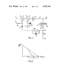
- FIG. 2 is a Bode plot of the circuit arrangement of FIG. 1;
- FIG. 3 is a circuit diagram of another of the AGC circuit arrangements.
- FIG. 4 is a circuit diagram of a further one of the AGC circuit arrangements.
- direct voltage signal components or constant amplitude signals are represented by upper case “V”, together with a distinguishing subscript, while varying amplitude components of such direct current or constant amplitude signals are represented by a lower case “v” together with a distinguishing subscript.
- the signal is passed to one terminal of a first modulator 6 which receives a modulating signal S c1 on a second input line 7.
- the output V 6 of the modulator 6 is passed to the first input of a second modulator 8 which receives a modulating signal S c2 on a second input line 12.
- the output V 8 of the second modulator 8 is passed through an amplifier 14 having an output line 16.
- the level of the signal V o on the line 16 is sensed by a detector 18 which produces a resultant output on a line 20 which is applied through a resistor R2 to a point 23.
- a reference signal S r is also applied to the point 23 . Therefore, the integrator input receives the algebraic sum of the signals applied to the point 23 through the resistors R2 and R3.
- Integrator 28 has an integrating capacitor C1 connected across it.
- the output S c of the integrator 28 provides the modulating signals S c1 and S c2 for the modulators 6 and 8.
- the signal S c1 is produced via a capacitor C2 which is shunted by a resistor R4 connected to a bias supply (not shown) by a terminal 32.
- the signal S c2 is produced via a resistor R5 which is shunted to ground by a capacitor C3. The result, therefore, is that the modulator 6 is responsive only to the alternating components of the signal S c , while the modulator 8 is responsive only to the D.C. and low frequency components of the signal S c .
- the output signal, V o of the circuit arrangement is taken from a terminal 36 connected to the line 16 from the amplifier 14.
- gain of amplifier 14 is A 1 ;
- V c1 is the bias voltage applied via resistor R 4 ;
- K 2 is the transfer characteristic of modulator 8.
- V 6 is constant and is the variation due to V c2 .
- FIG. 2 shows a Bode plot (loop gain against the logarithm of angular frequency) of Equation (9) where the angular frequencies ⁇ o , ⁇ 1 and ⁇ 3 correspond respectively to the time constants T o , T 1 and T 3 defined above.
- ⁇ 2 is the angular frequency at the upper end of the frequency band of the circuit.
- Equation (14) therefore shows the factors which affect ⁇ 2 that is, the factors which affect the upper limit of the bandwidth of the circuit. These factors are A 1 , A 2 , A 4 , K 1 and V i .
- a 4 will be reduced so as to hold V o constant. Therefore, for a given V o , A 1 .A 4 is constant.
- V i If now there is an increase in V i , then again, due to the D.C. feedback path through modulator 8, A 4 will be reduced to keep V o constant. Therefore, for a given V o , A 4 .V i is constant.
- a 2 the gain of the detector 18, must be constant (otherwise, the circuit arrangement will not be able to maintain V o constant).
- the factor K 1 for the modulator 6 should be constant.
- ⁇ 2 is constant.
- V o is constant. However it may be desired to operate the circuit arrangement so that V o varies (by a controlled amount). This may be done by varying the reference signal V r . However, a change in V r will produce a change (in the opposite sense) in V o . This is achieved by the variation of A 4 by means of the signal V c2 . Therefore, Equation (15) no longer applies, and thus ⁇ 2 is not constant if V o varies.
- Equation (15) shows that if A 2 can be made inversely proportional to V o , then A 2 ⁇ A 4 will be constant as V o varies. In such a case, ##EQU7## will be constant for all values of V o , and so, therefore, will ⁇ 2 .
- FIG. 3 shows the circuit arrangement of FIG. 1 modified in order to ensure that A 2 is inversely proportional to V o .
- the output of detector 18 is now fed through a resistor R 1 to ground, and an adjustable tapping on this resistor is fed through a buffer amplifier 40 to the resistor R 2 .
- the gain A 2 now becomes the overall gain of the sub-circuit comprising the detector 18, the resistor R 1 and the buffer amplifier 40.
- the reference V r is held constant (even when it is desired to vary V o ), and in order to change V o , adjustments are made to the position of the tapping on the resistor R 1 so as to alter the value of A 2 .
- a reduction in A 2 increases V o by producing a resultant increase in A 4 (via the control signal V c2 ).
- ⁇ 2 remains substantially constant for all values of V o (as well as for changes in the value of A 1 and V i ).
- FIG. 4 shows a modification to the circuit arrangement of FIG. 3 (but which can also be applied to the circuit arrangement of FIG. 1) in order to deal with this problem.
- the modification consists in the provision of by-pass circuits in series with the control inputs of the modulators 6 and 8, together with two additional resistors R 6 , R 7 .
- the by-pass circuits are provided by diodes D 1 , D 2 and D 3 .
- Diode D 3 is connected to the junction between the D 1 and D 2 which are respectively directly connected to the inputs of the modulators 6 and 8.
Landscapes
- Engineering & Computer Science (AREA)
- Multimedia (AREA)
- Control Of Amplification And Gain Control (AREA)
Abstract
An A.G.C. circuit is disclosed having two modulators connected in series to modulate an input signal and an amplifier for amplifying the output of the second modulator and applying it to an output terminal. A detector detects the output of the amplifier and an integrator compares the detected level with a reference so as to produce a control signal dependent on the error. The control signal is applied to the first modulator through an impedance path having an impedance which decreases with increasing frequency, and is applied to the same modulator through an impedance path having an impedance which increases with increasing frequency. In this way, the first modulator performs modulation primarily dependent on the A.C. component of the control signal and a second modulator performs modulation primarily dependent on its D.C. components of the control signal. Therefore, changes in the gain of the amplifier, or in the level of the input signal, which tend to alter the upper limit of the loop bandwidth of the circuit, are substantially offset by the effect of the resultant change in the gain of the second modulator.
Description
The invention relates to electrical circuit arrangements. One example of an electrical circuit arrangement to which the invention relates is an automatic gain control (AGC) circuit arrangement.
Various AGC circuit arrangements are known. However, a problem which can arise with known AGC circuit arrangements is that their bandwidth varies with gain and thus with the level of output signal for a given input. Where a wide loop bandwidth is required (e.g. to handle amplitude modulation up to 20 KHz or more), this variation of bandwidth can give rise to instability.
An object of the invention is an improved automatic gain control circuit arrangement.
A more specific object of the invention is an automatic gain control circuit arrangement having a bandwidth which is not unduly affected by the level of the input signal.
According to the invention, there is provided an automatic gain control circuit arrangement for producing an output signal which is dependent on an input signal and whose mean level has a desired value, comprising a signal path having an input for receiving the input signal and an output at which is produced the output signal, the signal path including control means controllable to vary the level of the signal in the signal path and amplifying means for amplifying the signal in the signal path, the circuit arrangement also including detecting means connected to sense the level of the signal in the signal path after its level has been varied by the control means and amplified by the amplifying means, and operative in response to variations of the sensed level from the desired value to produce a control signal dependent on the variations and which adjusts the control means in a sense such that it offsets the said variations, the control means comprising one part primarily responsive to the alternating component of the control signal and another part primarily responsive to the D.C. component of the control signal whereby changes in the gain of the amplifying means or in the level of the input signal which tend to alter the upper limit of the loop bandwidth of the circuit arrangement are substantially offset by the effect of the resultant change in the gain of the said other part of the control means.
According to the invention, there is also provided an automatic gain control circuit arrangement, comprising means for receiving an input signal, first modulating means connected to modulate the level of the input signal, second modulating means connected to modulate the output of the first modulating means, an amplifier for amplifying the output of the second modulating means and for applying it to an output terminal, a detector for detecting the level of the output of the amplifier, means operative to compare the detected level with a reference dependent on a desired value of the mean level of the signal produced at the output terminal whereby to produce a control signal dependent on the difference between the actual level of the output of the amplifier and the said desired value, the first and second frequency-dependent impedance paths of applying the control signal to the first and second modulating means respectively, one impedance path having an impedance which decreases with increasing frequency and the other impedance path having an impedance which increases with increasing frequency, whereby one modulating means performs modulation primarily dependent on the value of the alternating component of the control signal and the other modulating means performs modulation primarily dependent on the D.C. component of the control signal, so that the upper limit of the bandwidth of the circuit arrangement is substantially unaffected by changes in the gain of the amplifier or in the mean level of the input signal.
AGC circuit arrangements embodying the invention will now be described by way of example only and with reference to the accompanying diagrammatic drawings in which:
FIG. 1 is a circuit diagram of one of the AGC circuit arrangements;
FIG. 2 is a Bode plot of the circuit arrangement of FIG. 1;
FIG. 3 is a circuit diagram of another of the AGC circuit arrangements; and
FIG. 4 is a circuit diagram of a further one of the AGC circuit arrangements.
In the following description, direct voltage signal components or constant amplitude signals are represented by upper case "V", together with a distinguishing subscript, while varying amplitude components of such direct current or constant amplitude signals are represented by a lower case "v" together with a distinguishing subscript.
The AGC circuit arrangement (FIG. 1) has an input terminal 5 at which is received the input signal Si =Vi +vi. The signal is passed to one terminal of a first modulator 6 which receives a modulating signal Sc1 on a second input line 7. The output V6 of the modulator 6 is passed to the first input of a second modulator 8 which receives a modulating signal Sc2 on a second input line 12.
The output V8 of the second modulator 8 is passed through an amplifier 14 having an output line 16. The level of the signal Vo on the line 16 is sensed by a detector 18 which produces a resultant output on a line 20 which is applied through a resistor R2 to a point 23. Also applied to the point 23 is a reference signal Sr via a terminal 30 and a resistor R3. Therefore, the integrator input receives the algebraic sum of the signals applied to the point 23 through the resistors R2 and R3. Integrator 28 has an integrating capacitor C1 connected across it.
The output Sc of the integrator 28 provides the modulating signals Sc1 and Sc2 for the modulators 6 and 8. The signal Sc1 is produced via a capacitor C2 which is shunted by a resistor R4 connected to a bias supply (not shown) by a terminal 32. The signal Sc2 is produced via a resistor R5 which is shunted to ground by a capacitor C3. The result, therefore, is that the modulator 6 is responsive only to the alternating components of the signal Sc, while the modulator 8 is responsive only to the D.C. and low frequency components of the signal Sc.
The output signal, Vo, of the circuit arrangement is taken from a terminal 36 connected to the line 16 from the amplifier 14.
The AGC circuit of FIG. 1 will now be analysed. In the analysis which follows, the following terms will be used (in addition to those mentioned above):
S.sub.r =V.sub.r +V.sub.r ;
gain of amplifier 14 is A1 ;
gain of the detector 18 is A2 ;
S.sub.c =V.sub.c +v.sub.c
S.sub.c1 =V.sub.c1 +v.sub.c1
(where Vc1 is the bias voltage applied via resistor R4);
S.sub.c2 =V.sub.c2 +v.sub.c2 ;
the gain of modulator 6 (v6 /vi)=A3 ;
the gain of modulator 8 (v8 /v6)=A4 ; and
the values of the capacitors and resistors are taken to be represented by the references identifying them in FIG. 1.
Considering modulator 6,
v.sub.6 =A.sub.3 ·vi
but A3 =K1 ·Vc1 where K1 is the transfer characteristic of the modulator.
Therefore, ##EQU1## This assumes Vi is constant (vi =0).
Considering modulator 8, by analogy with Equation (1),
v.sub.8 =K.sub.2 ·V.sub.6 ·v.sub.c2 (2)
where K2 is the transfer characteristic of modulator 8.
But this assumes V6 is constant and is the variation due to Vc2. With Vc2 constant (vc2 =0) and V6 varying,
v.sub.8 =A.sub.4 ·v.sub.6 (3)
Therefore, combining Equations (2) and (3),
v.sub.8 =A.sub.4 ·v.sub.6 +K.sub.2 ·V.sub.6 ·v.sub.c2 (4)
Now, ##EQU2## Initially, it has been assumed that Vi is constant. Therefore vi =0. Under these conditions (and assuming Vr is constant, vr =0), the total loop gain G1 is ##EQU3## Substituting from Equations (1), (4) (6) and (7) into Equations (8), and assuming that C2 =C3 =C and R4 =R5 =R, ##EQU4##
FIG. 2 shows a Bode plot (loop gain against the logarithm of angular frequency) of Equation (9) where the angular frequencies ωo, ω1 and ω3 correspond respectively to the time constants To, T1 and T3 defined above. ω2 is the angular frequency at the upper end of the frequency band of the circuit.
By geometry from FIG. 2,
(ω.sub.3 /ω.sub.2)=(ω.sub.1 /ω.sub.o)
Therefore,
(T.sub.2 /T.sub.3)=(T.sub.o /T.sub.1)
Thus,
T.sub.2 =(T.sub.o ·T.sub.3 /T.sub.1) (13)
Substituting from Equations (10), (11) and (12) in Equations (13), ##EQU5##
Equation (14) therefore shows the factors which affect ω2 that is, the factors which affect the upper limit of the bandwidth of the circuit. These factors are A1, A2, A4, K1 and Vi.
The operation of the circuit arrangement will be considered assuming that it is desired to keep Vo constant, and that this will be done by keeping Vr constant.
If, now, there is an increase in A1, then, due to the D.C. feedback through the modulator 8, A4 will be reduced so as to hold Vo constant. Therefore, for a given Vo, A1.A4 is constant.
If now there is an increase in Vi, then again, due to the D.C. feedback path through modulator 8, A4 will be reduced to keep Vo constant. Therefore, for a given Vo, A4.Vi is constant.
Therefore, summarising, for a given Vo, A1.A4.Vi is constant.
In addition, A2, the gain of the detector 18, must be constant (otherwise, the circuit arrangement will not be able to maintain Vo constant).
Therefore, for a given Vo,
ω.sub.2 =Z.K.sub.1, ##EQU6##
For small values of control signal vc1, the factor K1 for the modulator 6 should be constant.
Therefore, overall, ω2 is constant.
The foregoing assumes that Vo is constant. However it may be desired to operate the circuit arrangement so that Vo varies (by a controlled amount). This may be done by varying the reference signal Vr. However, a change in Vr will produce a change (in the opposite sense) in Vo. This is achieved by the variation of A4 by means of the signal Vc2. Therefore, Equation (15) no longer applies, and thus ω2 is not constant if Vo varies.
However, Equation (15) shows that if A2 can be made inversely proportional to Vo, then A2 ·A4 will be constant as Vo varies. In such a case, ##EQU7## will be constant for all values of Vo, and so, therefore, will ω2.
FIG. 3 shows the circuit arrangement of FIG. 1 modified in order to ensure that A2 is inversely proportional to Vo. In the circuit of FIG. 3, the output of detector 18 is now fed through a resistor R1 to ground, and an adjustable tapping on this resistor is fed through a buffer amplifier 40 to the resistor R2. In this circuit, therefore, the gain A2 now becomes the overall gain of the sub-circuit comprising the detector 18, the resistor R1 and the buffer amplifier 40. In operation, the reference Vr is held constant (even when it is desired to vary Vo), and in order to change Vo, adjustments are made to the position of the tapping on the resistor R1 so as to alter the value of A2. Thus, a reduction in A2 increases Vo by producing a resultant increase in A4 (via the control signal Vc2).
Therefore, with the circuit arrangement of FIG. 3, ω2 remains substantially constant for all values of Vo (as well as for changes in the value of A1 and Vi).
In the circuit arrangements shown in FIGS. 1 and 3, a problem can arise at very low modulation frequency. Under these conditions, the impedance in the path for the signal Vc1 becomes significant and vc1 tends to zero and the signal Vc2 becomes effectively equal to Vc. Therefore, the modulator 8 must be capable of applying all the necessary modulation. For high levels of pulse modulation at these low frequencies, modulator 8 becomes overloaded and ineffective principally because the circuit limits the rate at which Vc2 can increase by charging capacitor C3.
FIG. 4 shows a modification to the circuit arrangement of FIG. 3 (but which can also be applied to the circuit arrangement of FIG. 1) in order to deal with this problem. The modification consists in the provision of by-pass circuits in series with the control inputs of the modulators 6 and 8, together with two additional resistors R6, R7. The by-pass circuits are provided by diodes D1, D2 and D3. Diode D3 is connected to the junction between the D1 and D2 which are respectively directly connected to the inputs of the modulators 6 and 8.
Normally, all these diodes are non-conducting.
However, at very low frequencies where C3 prevents Vc2 from changing sufficiently rapidly, the diodes D2 and D3 conduct therefore bypassing the effect of capacitor C3.
The mathematical analysis given above is in simplified form because it ignores the interaction between the modulators at the crossover frequency (i.e. the frequency where one modulator ceases to be effective and the other begins to become effective). However, this does not have any practical affect on the analysis at other frequencies and does not affect the constancy which the circuit arrangement gives to ω2 as explained above.
Claims (7)
1. An automatic gain control circuit arrangement for producing an output signal which is dependent on an input signal and whose mean level has a desired value, comprising
means defining a signal path having an input for receiving the input signal and an output at which is produced the output signal, the signal path including control means controllable to vary the level of the signal in the signal path and amplifying means for amplifying the signal in the signal path, and
detecting means connected to sense the level of the signal in the signal path after its level has been varied by the control means and amplified by the amplifying means, and operative in response to variations of the sensed level from the desired value to produce a control signal dependent on the variations and which adjusts the control means in a sense such that it offsets the said variations,
the control means comprising one part primarily responsive to the alternating component of the control signal and another part primarily responsive to the D.C. components of the control signal whereby changes in the gain of the amplifying means or in the level of the input signal which tend to alter the upper limit of the loop bandwidth of the circuit arrangement are substantially offset by the effect of the resultant change in the gain of the said other part of the control means.
2. A circuit arrangement according to claim 1, in which
one said part of the control means comprises first modulating means, having a control input for receiving the control signal via a first circuit path, the first circuit path including impedance means which decreases in impedance value with frequency, and
the other said part of the control means comprises second modulating means having a control input for receiving the control signal via a second circuit path, the second circuit path including impedance means which increases in impedance value with frequency.
3. A circuit arrangement according to claim 2, including bypass circuits respectively connected to bypass the said circuit paths of the first and second modulating means at very low frequencies.
4. A circuit arrangement according to claim 1, in which the detecting means comrises
a detector connected to sense the level of the signal in the signal path after its level has been varied by the control means and amplified by the amplifying means,
means producing a reference signal,
means connected to compare that level with the level of the reference signal whereby to produce the said control signal, and
means for adjusting the level of the reference signal whereby to adjust the desired value of the mean level of the output signal.
5. A circuit arrangement according to claim 1, in which the detecting means comprises
a detector having adjustable gain and connected to respond to the level of the signal in the signal path after its level has been varied by the control means and amplified by the amplifying means and operative to produce an output dependent on this level and on its said adjustable gain,
means producing a reference signal,
means for comparing this output with the reference signal whereby to produce the said control signal, and
means for adjusting the gain of the detector whereby to adjust the desired value of the mean level of the output signal.
6. A circuit arrangement according to claim 1, including integrating means connected to apply the control signal to the control means.
7. An automatic gain control circuit arrangement, comprising
means for receiving an input signal,
first modulating means connected to modulate the level of the input signal,
second modulating means connected to modulate the output of the first modulating means,
an amplifier amplifying the output of the second modulating means and for applying it to an output terminal,
a detector detecting the level of the output of the amplifier,
means producing a reference dependent on a desired value of the mean level of the signal produced at the output terminal,
means operative to compare the detected level with the reference whereby to produce a control signal dependent on the difference between the actual level of the output of the amplifier and the said desired value, and
first and second frequency-dependent impedance paths for applying the control signal to the first and second modulating means respectively,
one impedance path having an impedance which decreases with increasing frequency and the other impedance path having an impedance which increases with increasing frequency,
whereby one modulating means performs modulation primarily dependent on the value of the alternating component of the control signal and the other modulating means performs modulation primarily dependent on the D.C. component of the control signal, so that the upper limit of the bandwidth of the circuit arrangement is substantially unaffected by changes in the gain of the amplifier or in the mean level of the input signal.
Applications Claiming Priority (2)
| Application Number | Priority Date | Filing Date | Title |
|---|---|---|---|
| GB1643/79 | 1979-01-17 | ||
| GB7901643 | 1979-01-17 |
Publications (1)
| Publication Number | Publication Date |
|---|---|
| US4307348A true US4307348A (en) | 1981-12-22 |
Family
ID=10502559
Family Applications (1)
| Application Number | Title | Priority Date | Filing Date |
|---|---|---|---|
| US06/112,734 Expired - Lifetime US4307348A (en) | 1979-01-17 | 1980-01-17 | Automatic gain control circuit |
Country Status (1)
| Country | Link |
|---|---|
| US (1) | US4307348A (en) |
Cited By (5)
| Publication number | Priority date | Publication date | Assignee | Title |
|---|---|---|---|---|
| US4377788A (en) * | 1981-01-29 | 1983-03-22 | Rca Corporation | Signal expander |
| US4398157A (en) * | 1981-01-29 | 1983-08-09 | Rca Corporation | Signal expander/compressor with adaptive control circuit |
| US5208550A (en) * | 1991-04-16 | 1993-05-04 | Mitsubishi Denki Kabushiki Kaisha | Radio-frequency power amplifier device |
| US5237291A (en) * | 1991-06-19 | 1993-08-17 | Marconi Instruments Limited | Microwave frequency synthesizer having selectable oscillator sources and output power control |
| US5652547A (en) * | 1995-06-20 | 1997-07-29 | Motorola, Inc. | Current comparator automatic output control |
Citations (1)
| Publication number | Priority date | Publication date | Assignee | Title |
|---|---|---|---|---|
| GB951058A (en) * | 1959-04-23 | 1964-03-04 | Philips Electrical Ind Ltd | Improvements in or relating to amplifiers |
-
1980
- 1980-01-17 US US06/112,734 patent/US4307348A/en not_active Expired - Lifetime
Patent Citations (1)
| Publication number | Priority date | Publication date | Assignee | Title |
|---|---|---|---|---|
| GB951058A (en) * | 1959-04-23 | 1964-03-04 | Philips Electrical Ind Ltd | Improvements in or relating to amplifiers |
Cited By (5)
| Publication number | Priority date | Publication date | Assignee | Title |
|---|---|---|---|---|
| US4377788A (en) * | 1981-01-29 | 1983-03-22 | Rca Corporation | Signal expander |
| US4398157A (en) * | 1981-01-29 | 1983-08-09 | Rca Corporation | Signal expander/compressor with adaptive control circuit |
| US5208550A (en) * | 1991-04-16 | 1993-05-04 | Mitsubishi Denki Kabushiki Kaisha | Radio-frequency power amplifier device |
| US5237291A (en) * | 1991-06-19 | 1993-08-17 | Marconi Instruments Limited | Microwave frequency synthesizer having selectable oscillator sources and output power control |
| US5652547A (en) * | 1995-06-20 | 1997-07-29 | Motorola, Inc. | Current comparator automatic output control |
Similar Documents
| Publication | Publication Date | Title |
|---|---|---|
| CA2093844C (en) | Power detection technique for automatic amplifier power control | |
| US5208550A (en) | Radio-frequency power amplifier device | |
| US4853639A (en) | Non-contacting voltage metering apparatus | |
| CA2074124C (en) | Transmitter with nonlinearity correction circuits | |
| US4370622A (en) | IMD Limiter | |
| US4216434A (en) | Variable gain alternating voltage amplifier | |
| US4000472A (en) | Amplitude modulation envelope detector with temperature compensation | |
| US4119922A (en) | Circuit for automatic volume compression or volume expansion | |
| US2367110A (en) | Audio amplifier system | |
| US4307348A (en) | Automatic gain control circuit | |
| US2838742A (en) | Seismic gain control | |
| US4310243A (en) | Spectrophotometer with photomultiplier tube dark signal compensation | |
| US4209758A (en) | Method and apparatus for the automatic matching of a transmitter to an antenna | |
| US2866151A (en) | Voltage regulator with non-linear networks in control circuit | |
| US3105928A (en) | Self-optimizing servomechanisms | |
| US4166981A (en) | Continuous signal amplitude regulator | |
| US4088956A (en) | Automatic modulation percentage control for amplitude modulated transmitters | |
| CA1310377C (en) | Rf power-control circuit | |
| GB2066004A (en) | Automatic gain control circuits | |
| US4502015A (en) | Diode detector with linearity compensating circuit | |
| JPS59138111A (en) | Device for compensating temperature drift of gain of ultrahigh frequency electric signal amplifier | |
| US4312032A (en) | RF Power control apparatus | |
| GB2040616A (en) | Improvements in and Relating to Electrical Circuit Arrangements | |
| US3983505A (en) | Signal frequency band control system | |
| EP0266551B1 (en) | Non-contacting voltage metering apparatus |
Legal Events
| Date | Code | Title | Description |
|---|---|---|---|
| STCF | Information on status: patent grant |
Free format text: PATENTED CASE |