US4232245A - Reduced blooming devices - Google Patents
Reduced blooming devices Download PDFInfo
- Publication number
- US4232245A US4232245A US05/838,713 US83871377A US4232245A US 4232245 A US4232245 A US 4232245A US 83871377 A US83871377 A US 83871377A US 4232245 A US4232245 A US 4232245A
- Authority
- US
- United States
- Prior art keywords
- wafer
- region
- along
- bulk
- charge storage
- Prior art date
- Legal status (The legal status is an assumption and is not a legal conclusion. Google has not performed a legal analysis and makes no representation as to the accuracy of the status listed.)
- Expired - Lifetime
Links
Images


Classifications
-
- H—ELECTRICITY
- H01—ELECTRIC ELEMENTS
- H01J—ELECTRIC DISCHARGE TUBES OR DISCHARGE LAMPS
- H01J29/00—Details of cathode-ray tubes or of electron-beam tubes of the types covered by group H01J31/00
- H01J29/02—Electrodes; Screens; Mounting, supporting, spacing or insulating thereof
- H01J29/10—Screens on or from which an image or pattern is formed, picked up, converted or stored
- H01J29/36—Photoelectric screens; Charge-storage screens
- H01J29/39—Charge-storage screens
- H01J29/45—Charge-storage screens exhibiting internal electric effects caused by electromagnetic radiation, e.g. photoconductive screen, photodielectric screen, photovoltaic screen
- H01J29/451—Charge-storage screens exhibiting internal electric effects caused by electromagnetic radiation, e.g. photoconductive screen, photodielectric screen, photovoltaic screen with photosensitive junctions
- H01J29/453—Charge-storage screens exhibiting internal electric effects caused by electromagnetic radiation, e.g. photoconductive screen, photodielectric screen, photovoltaic screen with photosensitive junctions provided with diode arrays
- H01J29/455—Charge-storage screens exhibiting internal electric effects caused by electromagnetic radiation, e.g. photoconductive screen, photodielectric screen, photovoltaic screen with photosensitive junctions provided with diode arrays formed on a silicon substrate
Definitions
- the invention relates to sensing devices incorporating single crystal semiconductor wafers.
- Sensing devices such as silicon vidicons and silicon intensifier tubes employ sensing elements or targets consisting of single crystal semiconductor wafers.
- the operation of such sensing elements in these devices is well known in the art.
- One problem associated with their operation is that certain elemental signal areas of the sensing elements may become overly excited by an incident image signal.
- charge carriers in excess of the signal handling capabilities of the wafer may be generated at certain localized regions of the sensing element or wafer.
- the excess charge carriers diffuse laterally to adjacent regions of the wafer, causing a loss of imaging capability in the neighboring regions of the wafer as evidenced by an undesired "blooming" or overloading of the target in the localized region.
- This potential barrier in normal operation allows a limited number of excited minority carriers to penetrate to the input signal sensing surface and then recombine, thereby maximizing the sensitivity of the device by permitting the greater majority of excited minority carriers to diffuse toward a charge storage region of the wafer along a major surface opposite the sensing surface of that wafer.
- the excess carriers accumulate at and overcome the potential barrier. These excess carriers are swept to the sensing surface where they quickly recombine due to the substantially increased recombination velocity along that surface, thereby avoiding lateral diffusion to other neighboring regions of the target.
- the energy level configuration (and the potential barrier) necessary for accomplishing the noted blooming reduction mechanism can be controlled by carefully depositing a fixed number of donors or acceptors to a specified depth of the sensing element or wafer by suitable techniques such as, for example, ion implantation.
- suitable techniques such as, for example, ion implantation.
- the sensitivity of the device to strongly absorbed input signals, such as blue or ultraviolet light, in particular, is reduced in accordance with the distance of the potential barrier to that surface.
- a sensing device includes a single crystal semiconductor wafer having a potential barrier with a controlled energy level configuration within about 1500 A from an input signal sensing surface.
- the sensing device also includes a means for passivating the energy level configuration along the input signal sensing surface to the wafer for avoiding surface effects which would otherwise effect the energy level configuration in the region of the potential barrier.
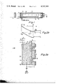
- FIG. 1 is a longitudinal sectional view of an improved vidicon camera tube utilizing the invention.
- FIGS. 2a and 3a are enlarged fragmentary sectional views of alternative sensing elements or targets suitable for use in the tube of FIG. 1.
- FIGS. 2b and 3b depict band diagrams showing the energy level configurations in the regions of the input signal sensing surface regions of the targets shown in FIGS. 2a and 3a, respectively.
- FIGS. 4 and 5 are enlarged fragmentary sectional views of alternative sensing elements or targets suitable for use in image intensifier tubes.
- FIG. 6 is a band diagram showing the energy level configuration associated with targets not employing the invention in the region of the input signal sensing surface.
- a preferred embodiment of the invention is a vidicon type camera tube 10 as shown in FIG. 1 having an evacuated envelope 12 and including a transparent faceplate 14 at one end of the envelope 12, and an electron gun assembly 16 inside the envelope 12 for forming a low velocity electron beam 18.
- An input signal sensing element or target 20, mounted on a ceramic spacer 22, is positioned adjacent the inside surface of the faceplate 14 in a manner suitable for receiving a light input image signal.
- Means (not shown) for magnetically focusing the beam 18 toward the target 20 and for causing the beam 18 to scan the surface of the target 20 may be disposed outside the envelope 12.
- the photon-excitable target 20, a fragment of which is shown in FIG. 2, is a wafer-shaped silicon photodiode target having a bulk region 24 of a single crystal of elemental silicon with first and second opposed major surfaces 26 and 28, respectively.
- the first major surface 26 comprises the input signal sensing surface of the target 20 for receiving on input light image.
- the second major surface 28 faces the electron beam, when mounted in the tube of FIG. 1, and is referred to, for simplicity, as the scan surface of wafer 24.
- the wafer 24 includes a charge storage region "B" along a surface portion including the scan surface 28, and and an input surface region "A" along the surface portion including the input signal sensing surface 26.
- the charge storage region “B” includes on the scan surface 28 of the silicon wafer 24, an array of discrete PN junction storage diodes 30.
- An insulating layer 32 of silicon dioxide is provided on the scan surface 28 between the discrete diodes 30 to shield the bulk 24 from the effects of the scanning electron beam 18.
- Contact pads 34 of P-type silicon are provided which cover the P-type surfaces of the discrete diodes 30 and overlap the insulating layer 32 about the periphery of the diode 30 in a manner well known in the art. Such pads 34 improve the contacts of the scanning beam 18 with the diodes 30.
- an energy level configuration of the silicon wafer 24 such as substantially shown in FIG. 2b.
- a P+ region 40 is provided along the input signal sensing surface 26 which effectively fixes the valence band E V in that region of the target 20 substantially at the Fermi level E F .
- An N+ potential barrier is provided a distance of C 1 from the input signal sensing surface 26 for accomplishing blooming control.
- C 1 represents the distance from the surface 26 to the peak of N+ distribution.
- the N+ potential barrier is preferably located such that C 1 is less than about 1500 A.
- the distribution of the doping profile in the region of the N+ potential barrier relative to the N-type bulk of the silicon wafer 24, should have the characteristics (B 1 and B 2 ) necessary for achieving the blooming reduction mechanism described in the aforementioned article by B. M. Singer et al.
- FIGS. 3a and 3b there is shown an alternative embodiment 120 of the target 20 (FIG. 2a) wherein similar numbers designate corresponding portions of each target except that the first digit of each designation number is varied to identify each of the various embodiments.
- a layer of transparent insulating material 136 along the input signal sensing surface 126 of the semiconductor wafer 124, including sufficient non-mobile negative charge 138 for inducing or causing an inversion behavior along that surface whereby a P+-like region is provided along the input signal sensing surface 26 by field-effect, effectively fixing the valence band E V in that surface region of the wafer 24, substantially at the Fermi level E F .
- the doped P+ region 40 shown in the embodiment of FIG. 2a is omitted.
- the target 20 is substantially similar to that shown in FIG. 2a.
- the energy level configuration of the target 120 extending into the bulk of the silicon wafer 24 from an exposed surface 127 of layer 136 is substantially as shown in FIG. 3b.
- the targets depicted in 2a-2b and 3a-3b may also be employed as electron excitable targets in silicon intensifier tubes.
- the operation and manufacture of silicon intensifier tubes is well known in the art of electron discharge devices.
- FIGS. 4 and 5 there is depicted other targets suitable for incorporation in such silicon intensifier tubes.
- the targets of FIGS. 4 and 5 are substantially similar to the targets in FIGS. 3a-3b and 2a-2b, respectively. Similar designation numbers are employed to designate corresponding portions of each target wherein the first digit of each designation number is varied to identify each of the various embodiments.
- FIGS. 3a-3b and 2a-2b In contrast to the targets depicted in FIGS. 3a-3b and 2a-2b, respectively, FIGS.
- a silicon wafer is, for example, first fabricated to include the charge storage region "B" previously described in the manner fully described in U.S. Pat. No. 3,548,233 issued to E. F. Cave et al on Dec. 15, 1970, and herein incorporated by reference.
- the details of construction of the charge storage regions of these sensing elements or targets 20, 120, 220 and 320 may be varied considerably without affecting the relevance of the instant invention.
- alternative charge storage regions "B" for theses targets may be fabricated by persons of ordinary skill in the art having the alternative structural configurations disclosed in U.S. Pat. No. 3,419,746 issued to M. H. Crowell et al on Dec. 31, 1968 and U.S. Pat. No. 3,403,284 issued to T. M. Buck et al on Sept. 24, 1968.
- the silicon wafers of targets 20, 120, 220 and 320 are now ion implanted with a suitable doping source to include the N+ potential barrier previously described.
- a suitable silicon wafer having a resistivity of 50 to 150 ohm-cm. bulk material with approximately 1 ⁇ 10 14 carriers per centimeters 3 may be processed to include a suitable N+ potential barrier in the following manner:
- the N+ potential barrier region may be implanted into such a wafer with the desired doping profile for controlling blooming using arsenic atoms with an incident energy of about 30 KeV.
- the peak doping in the resulting Gaussian-shaped profile at a distance C 1 from the input signal sensing surface of the wafer is about 1 ⁇ 10 18 atoms/cm 3 .
- These atoms are activated, for example, by heating or annealing the wafer in a furnace at a temperature of about 870° C. for a period of time of about 45 minutes. After such annealing, an effective active dopant level is achieved at the peak of the resultant potential barrier distribution by atoms which have become substitutional in the lattice for achieving the blooming control mechanism previously described.
- the silicon wafer 25 is further processed to include a suitable P+ region 40 along the input signal sensing surface 26.
- a suitable P+ surface region 40 of a thickness C 2 less than approximately 1,000 Angstroms thick, may be obtained by placing the silicon wafer in a boron diffusion furnace at between about 800°-900° C. for a period of time of about 5 minutes.
- the thickness of the P+ surface region 40 may be varied considerably so long as its dopant profile does not detrimentally affect the potential barrier and its characteristics (B 1 and B 2 ) necessary for achieving the blooming control function.
- the dopant level of the P+ layer is selected to substantially fix the valence band E V substantially at the Fermi level.
- the target 20 may be fabricated by techniques well known in the art.
- a layer of transparent insulating material 136 is evaporated along the surface 126 of the silicon wafer for producing an inversion-like behavior in the region of the silicon wafer interfacing therewith (i.e. a P+-like region).
- the target 120 is processed, subsequent to the ion implantation of the N+ potential barrier previously described, by placing the silicon wafer in an evacuation system including an electron gun evaporator for evaporating a suitable material for layer 136, such as, for example, a borosilicate glass (B 2 O 3 -S i O 2 ) to a thickness of about 500 Angstroms.
- borosilicate glass which is considered suitable, is for example, "Vycor” (a registered trademark) manufactured by Corning Glass Works of Corning, N.Y., having a composition consisting essentially of about 96% SiO 2 and about 3% B 2 O 3 .
- Such a material has been found to possess adequate non-mobile negative charge, after deposition, to achieve the desired inversion behavior in the wafer, previously described.
- the thickness of the layer 36 may be varied considerably without adversely affecting the performance of the target; however, the thickness and type of insulating material is preferably selected to minimize reflections in the blue end of the light spectrum.
- the targets depicted in FIGS. 4 and 5 are processed and fabricated substantially as described for the targets 120 and 20 shown in FIGS. 3a and 2a, respectively; however, an additional chromium buffer layer 242 or 342 is evaporated along the input signal sensing surfaces 226 or 326 as described in the aforementioned patent by W. N. Henry et al.
- sensing elements of the type described are desired wherein the potential barrier for providing blooming control is located about 1500 A or less from the input signal sensing surface in order to maximize sensitivity of the ultimate device, particularly to ultraviolet light.
- devices which have been manufactured with potential barriers located substantially at about 1500 A or less from the input signal sensing surface in contrast to those having similar operative potential barriers located substantially at 3000 A or more, have been found to have inadequate blooming control and/or other highly undesirable characteristics such as high dark current.
- Passivation refers to providing electrical stability of the energy level configuration (i.e. the relative positioning of E C and E V with respect to E F ) in the region adjacent the wafer's input signal sensing surface, by substantially fixing the relative position of the conduction and valence band relative to the Fermi-level.
- E V or E C is considered to be located substantially at the Fermi-level whenever C 3 (E F -E V ), or E C -E F , respectively, is less than about 0.1 eV.
- Passivation of sensing elements including a potential barrier less than about 1500 A from an input signal sensing surface may be provided by various means.
- the targets depicted in FIGS. 2a and 5 are passivated by providing a P+ region along surface 26 or 326, respectively, in the wafer 24, or 324, having a doping profile which fixes the valence band substantially at the Fermi-level.
- the targets depicted in FIGS. 3a and 4 include a layer of transparent insulating material 138, or 238, respectively, including sufficient non-mobile negative charge along the surface 126, or 226, to substantially fix the valence band at the Fermi-level along those surfaces.
- While the preferred embodiments of the invention relate to pickup tubes such as vidicons or image intensifier tubes, the invention encompasses other types of charge storage devices which have charge storage "input signal sensing elements" addressed by a reading means.
- Such devices may for example, comprise storage tubes, scan conversion tubes or solid state image sensors.
- the various modes of operation of the present invention as one of such devices and the voltages to be applied for such modes are well known to those skilled in the art and are discussed, for example, in the issued U.S. Pat. No. 3,403,284 to T. M. Buck et al mentioned earlier.
- the conductivity type of the discrete P regions and the N-type bulk region of the wafer 24 are reversed, so that the discrete regions are made N-type whereas the bulk regions of the wafer 24 is P-type.
- the conductivity type of the potential barrier is reversed (i.e. a P+ potential barrier is provided).
- the region 40 would be made N+ whereas the layer 136 in FIG. 3a would be made to include non-mobile positive charge.
- the energy level configuration would be stabilized along the input signal sensing surface by fixing the conduction band substantially at the Fermi-level.
- the energy level configuration is stabilized by providing a region of opposite conductivity type (or one similar in affect by inversion) to that of the bulk of the wafer along the signal sensing surface wherein the conducting band appropriate to the minority carriers excited in the bulk of the wafer is substantially fixed at the Fermi-level along that signal sensing surface.
- the scan side of the target 20 is brought to the potential of an accelerating mesh of the gun 18 by secondary emission.
- the wafer thickness be less than the average carrier diffusion length in the wafer. This assures that enough of the light generated carriers will be able to reach one of the discrete regions 30.
- the wafer should be made as thin as possible.
- the field free region of the wafer should preferably be minimized by applying voltages to the wafer which bring the depletion region associated with each of the discrete regions 30 to the point of location of the potential barrier implanted into the surface of the wafer. In this condition, light or electron excited carriers in the field-free region will be more likely to reach the depletion regions associated with each one of the discrete regions 30.
- an N+ type accumulation region for reducing surface recombination at the input signal sensing surface is not provided in the targets herein described.
- the input signal sensing surface may be supplied with an anti-reflective, or transparent coating to improve the optical coupling between the target and any associated objects such as the faceplate of the vidicon or image intensifier tubes within which it is included.
- the material selected for layer 136 is preferably made of an anti-reflective material.
- the reading of the target is accomplished by contacting the individual target elements such as the diodes of the array with an electron beam.
- the function of the electron beam may be performed by contacting each element with an electrical conductor and then scanning the conductors with solid state circuitry.
- the invention is applicable to targets from beam scanned devices, it is also applicable to solid state charge storage imaging devices such as CCD's and CID's.
- the invention may also be employed for passivating the input signal sensing surfaces of semiconductor sensing elements of single or multiple line array type imaging devices.
- the invention may be applied to any of such imaging and/or photon excitable devices wherein a potential barrier is provided within about 1500 A from an input signal sensing surface of a sensing element.
- sensing element is intended to broadly describe any element incorporating means for exciting charge carriers in accordance with electromagnetic energy (such as light in a photon-excitable device) or electrons (in an electron-excitable device) focused to impinge upon an input signal sensing surface of the element in the form of an image, without limitations as to the means of providing charge readout.
- electromagnetic energy such as light in a photon-excitable device
- electrons in an electron-excitable device
- Each of the embodiments described may be operated with voltages, currents and frequencies normally used for devices of the particular type.
- the targets are comparable with existing structures and do not require special treatment for successful operation.
Landscapes
- Physics & Mathematics (AREA)
- Electromagnetism (AREA)
- Solid State Image Pick-Up Elements (AREA)
- Transforming Light Signals Into Electric Signals (AREA)
Abstract
Description
Claims (12)
Priority Applications (1)
| Application Number | Priority Date | Filing Date | Title |
|---|---|---|---|
| US05/838,713 US4232245A (en) | 1977-10-03 | 1977-10-03 | Reduced blooming devices |
Applications Claiming Priority (1)
| Application Number | Priority Date | Filing Date | Title |
|---|---|---|---|
| US05/838,713 US4232245A (en) | 1977-10-03 | 1977-10-03 | Reduced blooming devices |
Related Parent Applications (1)
| Application Number | Title | Priority Date | Filing Date |
|---|---|---|---|
| US62075075A Continuation | 1975-10-08 | 1975-10-08 |
Publications (1)
| Publication Number | Publication Date |
|---|---|
| US4232245A true US4232245A (en) | 1980-11-04 |
Family
ID=25277864
Family Applications (1)
| Application Number | Title | Priority Date | Filing Date |
|---|---|---|---|
| US05/838,713 Expired - Lifetime US4232245A (en) | 1977-10-03 | 1977-10-03 | Reduced blooming devices |
Country Status (1)
| Country | Link |
|---|---|
| US (1) | US4232245A (en) |
Cited By (10)
| Publication number | Priority date | Publication date | Assignee | Title |
|---|---|---|---|---|
| US4329702A (en) * | 1980-04-23 | 1982-05-11 | Rca Corporation | Low cost reduced blooming device and method for making the same |
| US4358323A (en) * | 1980-04-23 | 1982-11-09 | Rca Corporation | Low cost reduced blooming device and method for making the same |
| JPS593982A (en) * | 1982-06-11 | 1984-01-10 | ア−ルシ−エ− コ−ポレ−ション | Imaging device and its manufacturing method |
| JPS59141266A (en) * | 1983-01-27 | 1984-08-13 | ア−ルシ−エ− コ−ポレ−シヨン | Image sensitive device |
| US4547957A (en) * | 1982-06-11 | 1985-10-22 | Rca Corporation | Imaging device having improved high temperature performance |
| US4603342A (en) * | 1983-01-03 | 1986-07-29 | Rca Corporation | Imaging array having higher sensitivity and a method of making the same |
| US4658497A (en) * | 1983-01-03 | 1987-04-21 | Rca Corporation | Method of making an imaging array having a higher sensitivity |
| US4665277A (en) * | 1986-03-11 | 1987-05-12 | The United States Of America As Represented By The Administrator Of The National Aeronautics And Space Administration | Floating emitter solar cell |
| US4689873A (en) * | 1983-04-28 | 1987-09-01 | Rca Corporation | Imaging device having two anti-reflection layers on a surface of silicon wafer |
| US5331165A (en) * | 1992-12-01 | 1994-07-19 | Ball Corporation | Split event reduced x-ray imager |
Citations (5)
| Publication number | Priority date | Publication date | Assignee | Title |
|---|---|---|---|---|
| US3548233A (en) * | 1968-11-29 | 1970-12-15 | Rca Corp | Charge storage device with pn junction diode array target having semiconductor contact pads |
| US3755015A (en) * | 1971-12-10 | 1973-08-28 | Gen Electric | Anti-reflection coating for semiconductor diode array targets |
| US3761762A (en) * | 1972-02-11 | 1973-09-25 | Rca Corp | Image intensifier camera tube having an improved electron bombardment induced conductivity camera tube target comprising a chromium buffer layer |
| US3786294A (en) * | 1971-02-22 | 1974-01-15 | Gen Electric | Protective coating for diode array targets |
| US3792197A (en) * | 1972-07-31 | 1974-02-12 | Bell Telephone Labor Inc | Solid-state diode array camera tube having electronic control of light sensitivity |
-
1977
- 1977-10-03 US US05/838,713 patent/US4232245A/en not_active Expired - Lifetime
Patent Citations (5)
| Publication number | Priority date | Publication date | Assignee | Title |
|---|---|---|---|---|
| US3548233A (en) * | 1968-11-29 | 1970-12-15 | Rca Corp | Charge storage device with pn junction diode array target having semiconductor contact pads |
| US3786294A (en) * | 1971-02-22 | 1974-01-15 | Gen Electric | Protective coating for diode array targets |
| US3755015A (en) * | 1971-12-10 | 1973-08-28 | Gen Electric | Anti-reflection coating for semiconductor diode array targets |
| US3761762A (en) * | 1972-02-11 | 1973-09-25 | Rca Corp | Image intensifier camera tube having an improved electron bombardment induced conductivity camera tube target comprising a chromium buffer layer |
| US3792197A (en) * | 1972-07-31 | 1974-02-12 | Bell Telephone Labor Inc | Solid-state diode array camera tube having electronic control of light sensitivity |
Non-Patent Citations (3)
| Title |
|---|
| Douglas, "High Light-Level Blooming in Silicon Vidicon," IEEE Trans. on Electron Devices, vol. ED-22, #5, May, 1975. * |
| Noda, et al., "An Economical Color Television Camera Utilizing a Silicon Vidicon for Electronic Color Separation," IEEE Trans. on Electron Devices, vol. ED-22, #5, May, 1975. * |
| Singer, et al., "Theory, Design, and Performance of Low-Blooming Silicon Diode Array Imaging Targets," IEEE Trans. on Electron Devices, vol. ED-21, #1, Jan., 1974. * |
Cited By (11)
| Publication number | Priority date | Publication date | Assignee | Title |
|---|---|---|---|---|
| US4329702A (en) * | 1980-04-23 | 1982-05-11 | Rca Corporation | Low cost reduced blooming device and method for making the same |
| US4358323A (en) * | 1980-04-23 | 1982-11-09 | Rca Corporation | Low cost reduced blooming device and method for making the same |
| JPS593982A (en) * | 1982-06-11 | 1984-01-10 | ア−ルシ−エ− コ−ポレ−ション | Imaging device and its manufacturing method |
| US4547957A (en) * | 1982-06-11 | 1985-10-22 | Rca Corporation | Imaging device having improved high temperature performance |
| US4603342A (en) * | 1983-01-03 | 1986-07-29 | Rca Corporation | Imaging array having higher sensitivity and a method of making the same |
| US4658497A (en) * | 1983-01-03 | 1987-04-21 | Rca Corporation | Method of making an imaging array having a higher sensitivity |
| JPS59141266A (en) * | 1983-01-27 | 1984-08-13 | ア−ルシ−エ− コ−ポレ−シヨン | Image sensitive device |
| US4521713A (en) * | 1983-01-27 | 1985-06-04 | Rca Corporation | Silicon target support assembly for an image sensing device |
| US4689873A (en) * | 1983-04-28 | 1987-09-01 | Rca Corporation | Imaging device having two anti-reflection layers on a surface of silicon wafer |
| US4665277A (en) * | 1986-03-11 | 1987-05-12 | The United States Of America As Represented By The Administrator Of The National Aeronautics And Space Administration | Floating emitter solar cell |
| US5331165A (en) * | 1992-12-01 | 1994-07-19 | Ball Corporation | Split event reduced x-ray imager |
Similar Documents
| Publication | Publication Date | Title |
|---|---|---|
| US3814968A (en) | Solid state radiation sensitive field electron emitter and methods of fabrication thereof | |
| US3894332A (en) | Solid state radiation sensitive field electron emitter and methods of fabrication thereof | |
| US4760031A (en) | Producing CCD imaging sensor with flashed backside metal film | |
| US3548233A (en) | Charge storage device with pn junction diode array target having semiconductor contact pads | |
| US4687922A (en) | Image detector operable in day or night modes | |
| JP3441101B2 (en) | Electron tube | |
| WO1998020561A9 (en) | Low-resistivity photon-transparent window attached to photo-sensitive silicon detector | |
| US5005063A (en) | CCD imaging sensor with flashed backside metal film | |
| EP0950264A1 (en) | Low-resistivity photon-transparent window attached to photo-sensitive silicon detector | |
| US4801994A (en) | Semiconductor electron-current generating device having improved cathode efficiency | |
| US4232245A (en) | Reduced blooming devices | |
| US3523208A (en) | Image converter | |
| US3676727A (en) | Diode-array target including isolating low resistivity regions | |
| US3983574A (en) | Semiconductor devices having surface state control | |
| US5365092A (en) | Frontside illuminated charge-coupled device with high sensitivity to the blue, ultraviolet and soft X-ray spectral range | |
| US4329702A (en) | Low cost reduced blooming device and method for making the same | |
| US3973270A (en) | Charge storage target and method of manufacture | |
| EP0178664A2 (en) | Solid state image sensing device and method for making the same | |
| US5399882A (en) | Camera device and method of manufacturing the same | |
| US4228446A (en) | Reduced blooming device having enhanced quantum efficiency | |
| US4547957A (en) | Imaging device having improved high temperature performance | |
| US4689873A (en) | Imaging device having two anti-reflection layers on a surface of silicon wafer | |
| US4358323A (en) | Low cost reduced blooming device and method for making the same | |
| US3956025A (en) | Semiconductor devices having surface state control and method of manufacture | |
| US3748549A (en) | Resistive sea for camera tube employing silicon target with array of diodes |
Legal Events
| Date | Code | Title | Description |
|---|---|---|---|
| AS | Assignment |
Owner name: NPD SUBSIDIARY INC., 38 Free format text: ASSIGNMENT OF ASSIGNORS INTEREST.;ASSIGNOR:RCA CORPORATION;REEL/FRAME:004815/0001 Effective date: 19870625 |
|
| AS | Assignment |
Owner name: BANCBOSTON FINANCIAL COMPANY Free format text: SECURITY INTEREST;ASSIGNOR:BURLE INDUSTRIES, INC., A CORP. OF PA;REEL/FRAME:004940/0952 Effective date: 19870714 Owner name: BURLE TECHNOLOGIES, INC., A CORP. OF DE Free format text: ASSIGNMENT OF ASSIGNORS INTEREST.;ASSIGNOR:BURLE INDUSTRIES, INC., A CORP. OF PA;REEL/FRAME:004940/0962 Effective date: 19870728 Owner name: BURLE INDUSTRIES, INC. Free format text: MERGER;ASSIGNOR:NPD SUBSIDIARY, INC., 38;REEL/FRAME:004940/0936 Effective date: 19870714 |
|
| AS | Assignment |
Owner name: BANCBOSTON FINANCIAL COMPANY, A MA BUSINESS TRUST Free format text: SECURITY INTEREST;ASSIGNOR:BURLE TECHNOLOGIES, INC., A DE CORPORATION;REEL/FRAME:005707/0021 Effective date: 19901211 |