US4081763A - Electroluminescent laser - Google Patents
Electroluminescent laser Download PDFInfo
- Publication number
- US4081763A US4081763A US05/760,581 US76058177A US4081763A US 4081763 A US4081763 A US 4081763A US 76058177 A US76058177 A US 76058177A US 4081763 A US4081763 A US 4081763A
- Authority
- US
- United States
- Prior art keywords
- electrodes
- active element
- laser
- mirrors
- capacitor
- Prior art date
- Legal status (The legal status is an assumption and is not a legal conclusion. Google has not performed a legal analysis and makes no representation as to the accuracy of the status listed.)
- Expired - Lifetime
Links
- 230000005284 excitation Effects 0.000 claims abstract description 16
- 239000003990 capacitor Substances 0.000 claims abstract description 15
- 239000000126 substance Substances 0.000 claims abstract description 12
- 230000005684 electric field Effects 0.000 claims abstract description 9
- 150000002500 ions Chemical class 0.000 claims abstract 6
- 239000000969 carrier Substances 0.000 claims abstract 3
- 239000011572 manganese Substances 0.000 claims description 11
- XOLBLPGZBRYERU-UHFFFAOYSA-N tin dioxide Chemical compound O=[Sn]=O XOLBLPGZBRYERU-UHFFFAOYSA-N 0.000 claims description 8
- 239000000843 powder Substances 0.000 claims description 7
- 229910001635 magnesium fluoride Inorganic materials 0.000 claims description 4
- PWHULOQIROXLJO-UHFFFAOYSA-N Manganese Chemical compound [Mn] PWHULOQIROXLJO-UHFFFAOYSA-N 0.000 claims description 2
- 238000007654 immersion Methods 0.000 claims description 2
- 229910052748 manganese Inorganic materials 0.000 claims description 2
- 230000005855 radiation Effects 0.000 claims 3
- 239000000758 substrate Substances 0.000 description 14
- 239000000463 material Substances 0.000 description 9
- 238000000034 method Methods 0.000 description 7
- OAICVXFJPJFONN-UHFFFAOYSA-N Phosphorus Chemical compound [P] OAICVXFJPJFONN-UHFFFAOYSA-N 0.000 description 5
- 239000012212 insulator Substances 0.000 description 5
- 239000004020 conductor Substances 0.000 description 4
- 239000013078 crystal Substances 0.000 description 4
- 239000010931 gold Substances 0.000 description 4
- 239000012535 impurity Substances 0.000 description 4
- 238000000151 deposition Methods 0.000 description 3
- 238000009792 diffusion process Methods 0.000 description 3
- 238000001704 evaporation Methods 0.000 description 3
- 230000008020 evaporation Effects 0.000 description 3
- 239000011521 glass Substances 0.000 description 3
- PCHJSUWPFVWCPO-UHFFFAOYSA-N gold Chemical compound [Au] PCHJSUWPFVWCPO-UHFFFAOYSA-N 0.000 description 3
- 229910052737 gold Inorganic materials 0.000 description 3
- 229910052751 metal Inorganic materials 0.000 description 3
- 239000002184 metal Substances 0.000 description 3
- 239000012190 activator Substances 0.000 description 2
- 238000006243 chemical reaction Methods 0.000 description 2
- 230000008021 deposition Effects 0.000 description 2
- 239000003989 dielectric material Substances 0.000 description 2
- 238000004519 manufacturing process Methods 0.000 description 2
- 229910052761 rare earth metal Inorganic materials 0.000 description 2
- 239000013543 active substance Substances 0.000 description 1
- 238000000137 annealing Methods 0.000 description 1
- WUKWITHWXAAZEY-UHFFFAOYSA-L calcium difluoride Chemical compound [F-].[F-].[Ca+2] WUKWITHWXAAZEY-UHFFFAOYSA-L 0.000 description 1
- 229910001634 calcium fluoride Inorganic materials 0.000 description 1
- 230000006835 compression Effects 0.000 description 1
- 238000007906 compression Methods 0.000 description 1
- 238000005401 electroluminescence Methods 0.000 description 1
- 238000001093 holography Methods 0.000 description 1
- 238000002347 injection Methods 0.000 description 1
- 239000007924 injection Substances 0.000 description 1
- 239000011159 matrix material Substances 0.000 description 1
- 230000005693 optoelectronics Effects 0.000 description 1
- 239000010453 quartz Substances 0.000 description 1
- 239000004065 semiconductor Substances 0.000 description 1
- VYPSYNLAJGMNEJ-UHFFFAOYSA-N silicon dioxide Inorganic materials O=[Si]=O VYPSYNLAJGMNEJ-UHFFFAOYSA-N 0.000 description 1
- 230000003595 spectral effect Effects 0.000 description 1
- 238000001228 spectrum Methods 0.000 description 1
- 230000002269 spontaneous effect Effects 0.000 description 1
- 230000007704 transition Effects 0.000 description 1
- 239000012780 transparent material Substances 0.000 description 1
- 238000007738 vacuum evaporation Methods 0.000 description 1
Images

Classifications
-
- H—ELECTRICITY
- H01—ELECTRIC ELEMENTS
- H01S—DEVICES USING THE PROCESS OF LIGHT AMPLIFICATION BY STIMULATED EMISSION OF RADIATION [LASER] TO AMPLIFY OR GENERATE LIGHT; DEVICES USING STIMULATED EMISSION OF ELECTROMAGNETIC RADIATION IN WAVE RANGES OTHER THAN OPTICAL
- H01S3/00—Lasers, i.e. devices using stimulated emission of electromagnetic radiation in the infrared, visible or ultraviolet wave range
- H01S3/09—Processes or apparatus for excitation, e.g. pumping
-
- H—ELECTRICITY
- H01—ELECTRIC ELEMENTS
- H01S—DEVICES USING THE PROCESS OF LIGHT AMPLIFICATION BY STIMULATED EMISSION OF RADIATION [LASER] TO AMPLIFY OR GENERATE LIGHT; DEVICES USING STIMULATED EMISSION OF ELECTROMAGNETIC RADIATION IN WAVE RANGES OTHER THAN OPTICAL
- H01S3/00—Lasers, i.e. devices using stimulated emission of electromagnetic radiation in the infrared, visible or ultraviolet wave range
- H01S3/05—Construction or shape of optical resonators; Accommodation of active medium therein; Shape of active medium
- H01S3/06—Construction or shape of active medium
- H01S3/063—Waveguide lasers, i.e. whereby the dimensions of the waveguide are of the order of the light wavelength
- H01S3/0632—Thin film lasers in which light propagates in the plane of the thin film
-
- H—ELECTRICITY
- H01—ELECTRIC ELEMENTS
- H01S—DEVICES USING THE PROCESS OF LIGHT AMPLIFICATION BY STIMULATED EMISSION OF RADIATION [LASER] TO AMPLIFY OR GENERATE LIGHT; DEVICES USING STIMULATED EMISSION OF ELECTROMAGNETIC RADIATION IN WAVE RANGES OTHER THAN OPTICAL
- H01S5/00—Semiconductor lasers
- H01S5/30—Structure or shape of the active region; Materials used for the active region
Definitions
- the invention relates to lasers and in particular to solid-state lasers for use in quantum electronics, computer devices, optoelectronics, holography and display devices.
- a solid-state injection laser employing a p-n junction monocrystal as an active element is known in the art.
- the facets of the crystal which are normal to the junction are polished to serve as mirrors of a Fabry-Perot cavity.
- the monocrystal is located between two excitation electrodes which is energized by a required voltage in order to excite the active element.
- This laser suffers from a number of drawbacks, vis. the small size of the emission surface (about 1 sq.mm); also high current densities in the generation mode (the threshold current is about 100 A/cm 2 at 4.2° K and 10 5 A/cm 2 at the room temperature); no generation at room temperature under the conditions of continuous excitation.
- the object of the present invention is to provide a solid-state laser having a large emission surface and low current densities in the generation mode which is able to operate at the room temperature under the conditions of continuous excitation and which assures a high efficiency of converting electric energy into light energy.
- a solid-state laser which comprises a Fabry-Perot cavity having an active element excited by an electric field that is produced by a voltage being applied to the excitation electrodes having the active element located between them and which, according to the invention, is arranged around a so called electroluminescent capacitor with the layer of the electroluminescent material of said capacitor being optically homogeneous and being doped with elements having unfilled electron shells and which serves as the active element of the laser while the electrodes of the capacitor perform the functions of Fabry-Perot cavity mirrors and those of the active element excitation, with one of them being partially transparent to the laser emission.
- the active element be made in the form of a film.
- the preferred material for said film is ZnS:Mn.
- the active element may be made as a crystal having plane-parallel facets.
- the active element could use a powder in an immersion medium which serves as a dielectric material transparent to the laser emission whose refractive index is equal to that of said powder.
- the partially transparent electrode mirrors as a structure consisting of a number of interlaced layers having high and low refractive indices, which would have a high refraction coefficient for the laser emission wavelength, and a layer of a conductive material which would be transparent to the laser emission.
- the multi-layer structure should be made of interlaced ZnS, and MgF 2 ; and the layer of the conductive material be made of a SnO 2 film.
- the proposed solid-state laser possesses a number of advantages, the major of them being: a simple design, a small size, low-cost for the materials, the efficiency of the conversion of electric energy to light energy said conversion being almost equal to unity with a low current threshold, which are attributed to the method of obtaining the inverse population through the impact excitation of the impurity centres under the conditions of the electrical fields direct excitation.
- the laser has a wide emission surface which can have an area of scores of square centimeters. It also makes it possible to obtain generation at the room temperature.
- FIG. 1 is a cross section of a solid-state laser according to the invention
- FIG. 2 is a cross section of another embodiment of the solid-state laser according to the invention.
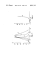
- FIG. 3 presents spectral characteristics illustrating the performance of a particular embodiment of the proposed solid-state laser
- FIG. 4 shows the relationship between the specific power of the laser emission and the excitation level.
- the solid-state laser shown schematically in FIG. 1 comprises a substrate 1 and an electroluminescent capacitor placed onto the substrate which is formed by a lower electrode 2 applied to the substrate 1 and an upper electrode 3 both made of a highly reflective material and serving also as the Fabry-Perot cavity mirrors. Between the electrodes a layer of electroluminescent substance is located which comprises an active element 4 of the laser, a protection layer 5 and an insulator layer 6.
- the substrate 1 should have a mirror-like surface and should be able to withstand the temperatures encountered in the process of depositing the electroluminescent material. If the laser emission is brought out through the substrate 1, the latter shall be made of transparent materials, e.g. glass, quartz crystal, etc.
- the functions of the substrate 1 can be performed by a plate of a highly reflective metal having a mirror-like surface which simultaneously serves as the lower mirror of the cavity.
- the active element 4 of the laser should be made of an optically homogeneous electroluminescent substance. Suitable for this purpose are substances doped with elements having unfilled electron shells, e.g., the transition or rare-earth elements in which it is possible to produce inverse populations in the impurity levels through out the electric field excitation.
- wide-zone high-resistance semiconductors such as ZnS:Mn, should be used for this purpose.
- the active element 4 can be made by applying a film or a powder onto the mirror substrate, with the powder being immersed into a medium of a dielectric material which is transparent to the laser emission whose refractive index is equal to that of the powder.
- the active element 4 can also be designed as a crystal having plane-parallel polished facets. In this case the substrate 1 is excluded from the design.
- the electrode mirrors 2 and 3 are made as layers of a conductive and a highly reflective material.
- the emission is brought out through the electrode mirrors 5 which is partially transparent to this emission.
- the electrode mirror 2 and 3 are designed either as continuous members or as intermittent pieces consisting of areas which are electrically isolated from one another and have preset sizes and shapes, e.g. rectangles, circles, segments, certain symbols or systems of parallel stripes. Such arrangements allows for multiple sources of stimulated emission of a required geometry on a single substrate to be obtained as well as flat matrix or mosaic screens.
- the electrodes 2 and 3 are made of metal films, such as Al, or Au.
- the electrode mirros 2 may also be made as a polished plate of a highly reflective conductive material which can simultaneously perform the functions of the substrate 1.
- the protection layer 5 serves to prevent the mutual diffusion between the material of the electrode mirrors 3 and the electroluminescent substance referred to thereafter as a phosphor in the course of deposition of the latter.
- Materials that could be used to make the protection layer should meet a number of requirements imposed by the temperatures involved in the process of manufacturing the laser. These are: a low diffusion coefficient for the material of the electrode mirrors 3, chemical resistance to the substances used for the layers adjacent to the protection layer 5, a low rate of diffusion of its components into the layer of the phosphor.
- Suitable substances for the protection layer are, for example, SiO, Tn 2 O 5 , CaF 2 .
- the protection layer should be made of a recrystallized film of an undoped basic phosphor substance, e.g. a ZnS film.
- the protection layer 5 should be made as thin as possible in order to reduce the voltage drop that occurs across it.
- the insulator layer 6 performs the same function as in ordinary electroluminescent films, i.e., it prevents the short circuiting of the phosphor layer in the process of deposition of the upper mirrors 3, thus raising the break down level of the electric field strength in the laser.
- This layer is made as an insulator film (for instance, SiO) whose thickness is much smaller than that of the active element 4.
- FIG. 2 shows another embodiment of a solid-state laser made as an electroluminescent capacitor which is applied onto a substrate 1.
- the electrode mirrors 2 and 3 are arranged as multi-layer structures consisting of interlaced layers 7,8,9 and 10,11,12 having high and low refractive indices and of layers 13 and 14 (one for each structure) made of a conductive material which is transparent to the laser emission.
- An active element 4 is placed between the structures.
- the multi-layer structures should have a high reflection coefficient at the laser emission wavelength.
- the layers 7,8,9 and 10,11,12 can be made of ZnS and MgF 2 or of ZnS and Na 3 AlF 6 . They should be arranged interdigitally.
- the layers 13 and 14 can be made as transparent films of a conductive substance selected from the SnO 2 , In 2 O 3 , CdO, ZnO group.
- the number of layers in the above mentioned structures can exceed the number of three as is shown in FIG. 2.
- the lower and upper electrode mirrors 2 and 3 respectively can have various numbers of interlaced layers havng high and low refractive indices, the actual number depends upon which is partially transparent and used to transmit the laser emission.
- the layers 13 and 14 can be arranged so that the layers 7,8,9 and 10,11,12 as well as the active element 4 are located between them or so that placed between them are either the layers 7,8,9 (or 10,11,12) and the active element 4, or only the active element 4.
- the two latter ways of arranging the layers 13 and 14 are preferable from the points of view of being able to lower the value of the laser operating voltage.
- the laser can be of a simpler design with a sufficiently high Q-factor for the cavity, where the non-transparent electrode is made as an opaque metal layer having a high reflection coefficient (for instance, an A1 film), while the partially transparent electrode mirrors is made as a multi-layer structure.
- the non-transparent electrode is made as an opaque metal layer having a high reflection coefficient (for instance, an A1 film)
- the partially transparent electrode mirrors is made as a multi-layer structure.
- the proposed solid-state laser operates as follows. A voltage from a power suply not shown in the drawing is applied to the electrode mirrors 2 and 3 (FIG. 1) or to the layers 13 and 14 (FIG. 2) which creates an intensive electric field (about 10 6 V/cm) in the active element 4, which is sufficient to produce impact excitation of the electroluminescence. When the excitation reaches its threshold level, the inverse population is created at the levels of the impurity centres (transistion or rare-earth elements) and the laser starts generating.
- the function of the Fabry-Perot cavity in the proposed laser embodiment is similar to that in the known devices. The wavelength of the laser emission depends on the type of phosphor and its doped impurity, as well as on the thickness of the active element 4 and on the angle at which the emission leaves the laser cavity.
- the proposed laser is arranged around thin (about 1 micron) ZnS:Mn electroluminescent films.
- the electrodes 2 and 3 are fed with an audio frequency effective voltage of 65 to 75 V.
- the laser emission is brought out through the lower electrode 2 and the substrate 1.
- the system being discussed would produce a spontaneous emission the spectrum of which is shown in FIG. 3 (curve 15) where the X-axis gives the wavelength in nanometers and Y-axis indicates the intensity of emissions related to the intensity at the maximum of a emission band.
- the emission band After the threshold of 60 V has been reached, the emission band would get considerably compressed and in the generation mode it half-width would be 6 to 8 nanometers (curve 16), which is one order of magnitude below the natural emission band ZnS:Mn (curve 17).
- the divergence angle of the laser emission in this case does not exceed 10°.
- the compression of the emission band is accompanied by a sharp increase of its power as illustrated by curve 18 (FIG. 4) where the X-axis shows the intensity of the electrical field in volts per centimeter and the Y-axis presents the specific power emission in milliwatts per square centimeter of the laser emission surface.
- the laser being described has been manufactured in the following way.
- a glass plane-parallel substrate 1 cleaned beforehand is used as a basis onto which a partially transparent gold layer is deposited by evaporation in a vacuum of (1+2) ⁇ 10 -5 torr.
- the reflection coefficient of the gold layer is 65 to 75%. It serves as an electrode 2 and at the same time as a Fabry-Perot cavity mirror.
- On undoped film of ZnS 150-200 nanometers thick is deposited onto it by evaporation in a vacuum of (1+2) ⁇ 10 -5 torr which serves as a protection layer 5. This film is crystallized by means of annealing same in a vacuum of 10 -5 torr at 550 to 600° C for 5 to 10 minutes.
- an electroluminescent film (the active element 4) of the ZnS:Mn active substance which is about 600 nanometers thick.
- the process consists of two steps. At first a ZnS film is applied by means of evaporation in a vacuum of 10 -5 torr. Simultaneously an Mn-activator is vaporized into this film. Then, the total layer is annealed in a vacuum of about 10 -5 torr at 650 to 670° C for 5 to 10 minutes.
- the film is crystallized and simultaneously the Mn activator becomes uniformly implanted into the ZnS lattice throughout the thickness of the film.
- the concentration of the implanted manganese is from 1 to 2 weight percent.
Landscapes
- Physics & Mathematics (AREA)
- Electromagnetism (AREA)
- Optics & Photonics (AREA)
- Engineering & Computer Science (AREA)
- Plasma & Fusion (AREA)
- Condensed Matter Physics & Semiconductors (AREA)
- General Physics & Mathematics (AREA)
- Electroluminescent Light Sources (AREA)
Abstract
A solid-state laser in which an inverse population is formed at the levels of dope ions of the elements with unfilled electron shells by means of impact excitation of said ions with hot carriers, made on the basis of an electroluminescent capacitor in which the layer of electroluminescent substance is optically homogeneous, doped with said elements, and serves as the active element of the laser. The electrodes of the capacitor perform the functions of the Fabry-Perot cavity mirrors and those of the electrodes in order to produce the electrical field required to excite the active element. One of these electrodes is partially transparent to the laser emission.
Description
This is a continuation of application Ser. No. 320,926, filed Jan. 4, 1973 and now abandoned.
The invention relates to lasers and in particular to solid-state lasers for use in quantum electronics, computer devices, optoelectronics, holography and display devices.
A solid-state injection laser employing a p-n junction monocrystal as an active element is known in the art. The facets of the crystal which are normal to the junction are polished to serve as mirrors of a Fabry-Perot cavity. The monocrystal is located between two excitation electrodes which is energized by a required voltage in order to excite the active element.
This laser suffers from a number of drawbacks, vis. the small size of the emission surface (about 1 sq.mm); also high current densities in the generation mode (the threshold current is about 100 A/cm2 at 4.2° K and 105 A/cm2 at the room temperature); no generation at room temperature under the conditions of continuous excitation.
The object of the present invention is to provide a solid-state laser having a large emission surface and low current densities in the generation mode which is able to operate at the room temperature under the conditions of continuous excitation and which assures a high efficiency of converting electric energy into light energy.
This object is achieved by providing a solid-state laser which comprises a Fabry-Perot cavity having an active element excited by an electric field that is produced by a voltage being applied to the excitation electrodes having the active element located between them and which, according to the invention, is arranged around a so called electroluminescent capacitor with the layer of the electroluminescent material of said capacitor being optically homogeneous and being doped with elements having unfilled electron shells and which serves as the active element of the laser while the electrodes of the capacitor perform the functions of Fabry-Perot cavity mirrors and those of the active element excitation, with one of them being partially transparent to the laser emission.
It is preferable that the active element be made in the form of a film.
The preferred material for said film is ZnS:Mn.
The active element may be made as a crystal having plane-parallel facets.
It is also feasible that the active element could use a powder in an immersion medium which serves as a dielectric material transparent to the laser emission whose refractive index is equal to that of said powder.
In the preferred embodiment of the invention, it is at least expedient to design the partially transparent electrode mirrors as a structure consisting of a number of interlaced layers having high and low refractive indices, which would have a high refraction coefficient for the laser emission wavelength, and a layer of a conductive material which would be transparent to the laser emission.
It is feasible that the multi-layer structure should be made of interlaced ZnS, and MgF2 ; and the layer of the conductive material be made of a SnO2 film.
The proposed solid-state laser possesses a number of advantages, the major of them being: a simple design, a small size, low-cost for the materials, the efficiency of the conversion of electric energy to light energy said conversion being almost equal to unity with a low current threshold, which are attributed to the method of obtaining the inverse population through the impact excitation of the impurity centres under the conditions of the electrical fields direct excitation. Besides, the laser has a wide emission surface which can have an area of scores of square centimeters. It also makes it possible to obtain generation at the room temperature.
The invention will be better understood from the description of its embodiments given by way of example with reference to the accompanying drawings, in which:
FIG. 1 is a cross section of a solid-state laser according to the invention;
FIG. 2 is a cross section of another embodiment of the solid-state laser according to the invention;
FIG. 3 presents spectral characteristics illustrating the performance of a particular embodiment of the proposed solid-state laser;
FIG. 4 shows the relationship between the specific power of the laser emission and the excitation level.
The solid-state laser shown schematically in FIG. 1 comprises a substrate 1 and an electroluminescent capacitor placed onto the substrate which is formed by a lower electrode 2 applied to the substrate 1 and an upper electrode 3 both made of a highly reflective material and serving also as the Fabry-Perot cavity mirrors. Between the electrodes a layer of electroluminescent substance is located which comprises an active element 4 of the laser, a protection layer 5 and an insulator layer 6.
The substrate 1 should have a mirror-like surface and should be able to withstand the temperatures encountered in the process of depositing the electroluminescent material. If the laser emission is brought out through the substrate 1, the latter shall be made of transparent materials, e.g. glass, quartz crystal, etc.
In case the emission is brought out through the upper mirror-electrode 3, the functions of the substrate 1 can be performed by a plate of a highly reflective metal having a mirror-like surface which simultaneously serves as the lower mirror of the cavity.
The active element 4 of the laser should be made of an optically homogeneous electroluminescent substance. Suitable for this purpose are substances doped with elements having unfilled electron shells, e.g., the transition or rare-earth elements in which it is possible to produce inverse populations in the impurity levels through out the electric field excitation.
It is preferable that wide-zone high-resistance semiconductors, such as ZnS:Mn, should be used for this purpose.
The active element 4 can be made by applying a film or a powder onto the mirror substrate, with the powder being immersed into a medium of a dielectric material which is transparent to the laser emission whose refractive index is equal to that of the powder.
The active element 4 can also be designed as a crystal having plane-parallel polished facets. In this case the substrate 1 is excluded from the design.
The electrode mirrors 2 and 3 are made as layers of a conductive and a highly reflective material.
In the laser embodiment under discussion, the emission is brought out through the electrode mirrors 5 which is partially transparent to this emission. The electrode mirror 2 and 3 are designed either as continuous members or as intermittent pieces consisting of areas which are electrically isolated from one another and have preset sizes and shapes, e.g. rectangles, circles, segments, certain symbols or systems of parallel stripes. Such arrangements allows for multiple sources of stimulated emission of a required geometry on a single substrate to be obtained as well as flat matrix or mosaic screens. The electrodes 2 and 3 are made of metal films, such as Al, or Au.
The electrode mirros 2 may also be made as a polished plate of a highly reflective conductive material which can simultaneously perform the functions of the substrate 1.
The protection layer 5 serves to prevent the mutual diffusion between the material of the electrode mirrors 3 and the electroluminescent substance referred to thereafter as a phosphor in the course of deposition of the latter. Materials that could be used to make the protection layer should meet a number of requirements imposed by the temperatures involved in the process of manufacturing the laser. These are: a low diffusion coefficient for the material of the electrode mirrors 3, chemical resistance to the substances used for the layers adjacent to the protection layer 5, a low rate of diffusion of its components into the layer of the phosphor. Suitable substances for the protection layer are, for example, SiO, Tn2 O5, CaF2. In case the active element 4 is made of ZnS:Mn, but it is feasible that the protection layer should be made of a recrystallized film of an undoped basic phosphor substance, e.g. a ZnS film. The protection layer 5 should be made as thin as possible in order to reduce the voltage drop that occurs across it.
The insulator layer 6 performs the same function as in ordinary electroluminescent films, i.e., it prevents the short circuiting of the phosphor layer in the process of deposition of the upper mirrors 3, thus raising the break down level of the electric field strength in the laser. This layer is made as an insulator film (for instance, SiO) whose thickness is much smaller than that of the active element 4.
FIG. 2 shows another embodiment of a solid-state laser made as an electroluminescent capacitor which is applied onto a substrate 1. In contrast with the embodiment described above and in order to increase the Q-factor of the cavity, the electrode mirrors 2 and 3 are arranged as multi-layer structures consisting of interlaced layers 7,8,9 and 10,11,12 having high and low refractive indices and of layers 13 and 14 (one for each structure) made of a conductive material which is transparent to the laser emission. An active element 4 is placed between the structures. The multi-layer structures should have a high reflection coefficient at the laser emission wavelength. The layers 7,8,9 and 10,11,12 can be made of ZnS and MgF2 or of ZnS and Na3 AlF6. They should be arranged interdigitally. The layers 13 and 14 can be made as transparent films of a conductive substance selected from the SnO2, In2 O3, CdO, ZnO group. The number of layers in the above mentioned structures can exceed the number of three as is shown in FIG. 2. The lower and upper electrode mirrors 2 and 3 respectively can have various numbers of interlaced layers havng high and low refractive indices, the actual number depends upon which is partially transparent and used to transmit the laser emission.
There can be different ways of arranging the conductive layers 13 and 14 with respect to the interlaced layers 7,8,9 and 10,11,12. The layers 13 and 14 can be arranged so that the layers 7,8,9 and 10,11,12 as well as the active element 4 are located between them or so that placed between them are either the layers 7,8,9 (or 10,11,12) and the active element 4, or only the active element 4. The two latter ways of arranging the layers 13 and 14 are preferable from the points of view of being able to lower the value of the laser operating voltage.
The laser can be of a simpler design with a sufficiently high Q-factor for the cavity, where the non-transparent electrode is made as an opaque metal layer having a high reflection coefficient (for instance, an A1 film), while the partially transparent electrode mirrors is made as a multi-layer structure.
The proposed solid-state laser operates as follows. A voltage from a power suply not shown in the drawing is applied to the electrode mirrors 2 and 3 (FIG. 1) or to the layers 13 and 14 (FIG. 2) which creates an intensive electric field (about 106 V/cm) in the active element 4, which is sufficient to produce impact excitation of the electroluminescence. When the excitation reaches its threshold level, the inverse population is created at the levels of the impurity centres (transistion or rare-earth elements) and the laser starts generating. The function of the Fabry-Perot cavity in the proposed laser embodiment is similar to that in the known devices. The wavelength of the laser emission depends on the type of phosphor and its doped impurity, as well as on the thickness of the active element 4 and on the angle at which the emission leaves the laser cavity.
A fuller understanding of the essence of the present invention may be had from the following description of an example of its embodiment, its operation and manufacturing procedure.
The proposed laser is arranged around thin (about 1 micron) ZnS:Mn electroluminescent films. A partially transparent gold layer is applied onto the glass plane-parallel substrate 1 having a reflection coefficient of R = 65 to 75% which simultaneously serves as the electrode 2 and a Fabry-Perot cavity mirror. It carries the protection layer 5 made as an undoped ZnS film 150 to 200 nanometers thick. Placed above the layer 5 is an electroluminescent ZnS film doped with Mn having a concentration of Mn-CMn = 1-2 weight percent and being within 0.6 to 1.0 micron thick (the active element). A Si0-insulator layer 6 being 20-25 nanometers thick is then placed and an opaque A1 film which serves as the second electrode 3 of the electroluminescent capacitor and at the same time as the upper Fabry-Perot cavity mirror. It has a reflection coefficient of R=90%. In operation, the electrodes 2 and 3 are fed with an audio frequency effective voltage of 65 to 75 V. The laser emission is brought out through the lower electrode 2 and the substrate 1. At a voltage below 60 V the system being discussed would produce a spontaneous emission the spectrum of which is shown in FIG. 3 (curve 15) where the X-axis gives the wavelength in nanometers and Y-axis indicates the intensity of emissions related to the intensity at the maximum of a emission band. After the threshold of 60 V has been reached, the emission band would get considerably compressed and in the generation mode it half-width would be 6 to 8 nanometers (curve 16), which is one order of magnitude below the natural emission band ZnS:Mn (curve 17). The divergence angle of the laser emission in this case does not exceed 10°. The compression of the emission band is accompanied by a sharp increase of its power as illustrated by curve 18 (FIG. 4) where the X-axis shows the intensity of the electrical field in volts per centimeter and the Y-axis presents the specific power emission in milliwatts per square centimeter of the laser emission surface.
The laser being described has been manufactured in the following way.
A glass plane-parallel substrate 1 cleaned beforehand is used as a basis onto which a partially transparent gold layer is deposited by evaporation in a vacuum of (1+2)×10-5 torr. The reflection coefficient of the gold layer is 65 to 75%. It serves as an electrode 2 and at the same time as a Fabry-Perot cavity mirror. On undoped film of ZnS 150-200 nanometers thick is deposited onto it by evaporation in a vacuum of (1+2)×10-5 torr which serves as a protection layer 5. This film is crystallized by means of annealing same in a vacuum of 10-5 torr at 550 to 600° C for 5 to 10 minutes. Placed above this layer is an electroluminescent film (the active element 4) of the ZnS:Mn active substance which is about 600 nanometers thick. The process consists of two steps. At first a ZnS film is applied by means of evaporation in a vacuum of 10-5 torr. Simultaneously an Mn-activator is vaporized into this film. Then, the total layer is annealed in a vacuum of about 10-5 torr at 650 to 670° C for 5 to 10 minutes.
During the procedure, the film is crystallized and simultaneously the Mn activator becomes uniformly implanted into the ZnS lattice throughout the thickness of the film. The concentration of the implanted manganese is from 1 to 2 weight percent. The vacuum evaporation process is then used to apply a SiO insulator layer 6 being 20 to 35 nanometers thick and an opaque A1 film having a reflection coefficient of R=90%, which serves as the second electrode 3 of the electroluminescent capacitor and as the upper mirror of the Fabry-Perot cavity.
Claims (3)
1. A solid-state laser with a Fabry-Perot cavity in which an inverted population is formed at the levels of dope ions which are elements having unfilled electron shells by means of impact excitation of said ions with carriers accelerated by an electric field, made on the basis of an electroluminescent capacitor and comprising:
an active element, which is a layer of an electroluminescent substance of said capacitor; which is optically homogeneous and doped with said elements having unfilled electron shells;
electrodes for said capacitor, between which said active element is disposed, said electrodes being intended to form an electric excitation field of said active element;
said electrodes being simultaneously the mirrors of a Fabry-Perot cavity, one of said electrode mirrors being partially transparent to the laser emission, a voltage being applied to said electrodes, wherein the active element is a powder placed in an immersion medium which is a dielectric transparent to the laser emission whose refractive index is equal to that of the powder.
2. A solid-state laser with a Fabry-Perot cavity in which an inverted population is formed at the levels of dope ions which are elements having unfilled electron shells by means of impact excitation of said ions with carriers accelerated by an electric field, made on the basis of an electroluminescent capacitor and comprising:
an active element, which is a layer of an electroluminescent substance of said capacitor;
which is optically homogeneous and doped with said elements having unfilled electron shells;
multi-layer structure electrodes for said capacitor, between which said active element is disposed, said electrodes being intended to form an electric excitation field of said active element, said electrodes being simultaneously the mirrors of a Fabry-Perot cavity, one of said electrode mirrors being partially transparent to the laser emission, a voltage being applied to said electrodes;
said multi-layer structure being made of interlaced ZnS and MgF2 layers and a SnO2 layer.
3. The apparatus of claim 2 wherein said active element is a ZnS film which is uniformly doped over its thickness with manganese;
said electrodes are made of SnO2 transparent to laser radiation;
and said mirrors of said cavity are comprised of a multi-layer structure of alternating layers of ZnS and MgF2, said mirrors having a high reflection coefficient for the wave length of laser radiation, said mirrors being arranged from each other at a distance which is a multiple of the wave length of radiation from said laser.
Applications Claiming Priority (1)
| Application Number | Priority Date | Filing Date | Title |
|---|---|---|---|
| US32092673A | 1973-01-04 | 1973-01-04 |
Related Parent Applications (1)
| Application Number | Title | Priority Date | Filing Date |
|---|---|---|---|
| US32092673A Continuation | 1973-01-04 | 1973-01-04 |
Publications (1)
| Publication Number | Publication Date |
|---|---|
| US4081763A true US4081763A (en) | 1978-03-28 |
Family
ID=23248442
Family Applications (1)
| Application Number | Title | Priority Date | Filing Date |
|---|---|---|---|
| US05/760,581 Expired - Lifetime US4081763A (en) | 1973-01-04 | 1977-01-19 | Electroluminescent laser |
Country Status (1)
| Country | Link |
|---|---|
| US (1) | US4081763A (en) |
Cited By (17)
| Publication number | Priority date | Publication date | Assignee | Title |
|---|---|---|---|---|
| US4161702A (en) * | 1977-09-28 | 1979-07-17 | The United States Of America As Represented By The Secretary Of The Navy | Distributed feedback filter and laser |
| US4309670A (en) * | 1979-09-13 | 1982-01-05 | Xerox Corporation | Transverse light emitting electroluminescent devices |
| US4737960A (en) * | 1986-09-26 | 1988-04-12 | American Telephone And Telegraph Company, At&T Bell Laboratories | Rare earth doped semiconductor laser |
| US4756606A (en) * | 1986-06-05 | 1988-07-12 | American Telephone And Telegraph Company, At&T Bell Laboratories | Apparatus comprising a monolithic nonlinear Fabry-Perot etalon, and method for producing same |
| EP0588327A1 (en) * | 1992-09-15 | 1994-03-23 | Texas Instruments Incorporated | Silicon-based microlaser by doped thin glass films |
| US5363398A (en) * | 1993-09-30 | 1994-11-08 | At&T Bell Laboratories | Absorption resonant rare earth-doped micro-cavities |
| US5541948A (en) * | 1994-11-28 | 1996-07-30 | The Regents Of The University Of California | Transition-metal doped sulfide, selenide, and telluride laser crystal and lasers |
| US5796120A (en) * | 1995-12-28 | 1998-08-18 | Georgia Tech Research Corporation | Tunnel thin film electroluminescent device |
| WO2000016454A1 (en) * | 1998-09-17 | 2000-03-23 | Astralux, Incorporated | Electroluminescent solid state device |
| US6565770B1 (en) | 2000-11-17 | 2003-05-20 | Flex Products, Inc. | Color-shifting pigments and foils with luminescent coatings |
| US6572784B1 (en) | 2000-11-17 | 2003-06-03 | Flex Products, Inc. | Luminescent pigments and foils with color-shifting properties |
| US20040027652A1 (en) * | 2002-07-31 | 2004-02-12 | Turan Erdogan | Optical filter and fluorescence spectroscopy system incorporating the same |
| US6806505B2 (en) * | 1998-07-23 | 2004-10-19 | Sony Corporation | Light emitting device and process for producing the same |
| US20050110999A1 (en) * | 2002-07-31 | 2005-05-26 | Turan Erdogan | Optical filter and fluorescence spectroscopy system incorporating the same |
| KR100696353B1 (en) * | 1998-07-23 | 2007-03-19 | 소니 가부시끼 가이샤 | Light emitting device and process for producing the same |
| CN101398950B (en) * | 2007-09-25 | 2010-12-22 | 中国印钞造币总公司 | Method for authenticating document of value |
| US20130301117A1 (en) * | 2012-05-11 | 2013-11-14 | Luis E. Zapata | Methods, systems, and apparatus for high energy optical-pulse amplification at high average power |
Citations (6)
| Publication number | Priority date | Publication date | Assignee | Title |
|---|---|---|---|---|
| US3046432A (en) * | 1960-10-19 | 1962-07-24 | Jr Richard B Nehrich | Electroluminescent light |
| US3248669A (en) * | 1962-10-30 | 1966-04-26 | Ibm | Semiconductor laser with optical cavity |
| US3268755A (en) * | 1961-03-30 | 1966-08-23 | Optische Ind De Oude Delft Nv | Current-electroluminescence device having a high resistance layer |
| US3431437A (en) * | 1964-05-25 | 1969-03-04 | Rca Corp | Optical system for performing digital logic |
| US3579130A (en) * | 1969-07-18 | 1971-05-18 | Vern N Smiley | Thin film active interference filter |
| US3621455A (en) * | 1970-07-28 | 1971-11-16 | Milton Green | Pinch effect laser |
-
1977
- 1977-01-19 US US05/760,581 patent/US4081763A/en not_active Expired - Lifetime
Patent Citations (6)
| Publication number | Priority date | Publication date | Assignee | Title |
|---|---|---|---|---|
| US3046432A (en) * | 1960-10-19 | 1962-07-24 | Jr Richard B Nehrich | Electroluminescent light |
| US3268755A (en) * | 1961-03-30 | 1966-08-23 | Optische Ind De Oude Delft Nv | Current-electroluminescence device having a high resistance layer |
| US3248669A (en) * | 1962-10-30 | 1966-04-26 | Ibm | Semiconductor laser with optical cavity |
| US3431437A (en) * | 1964-05-25 | 1969-03-04 | Rca Corp | Optical system for performing digital logic |
| US3579130A (en) * | 1969-07-18 | 1971-05-18 | Vern N Smiley | Thin film active interference filter |
| US3621455A (en) * | 1970-07-28 | 1971-11-16 | Milton Green | Pinch effect laser |
Non-Patent Citations (2)
| Title |
|---|
| Jvey, "Electroluminescence and Semiconductor Lasers", IEEE Jour. of Quantam Electronics, vol. QE-Z, pp. 713-26, Nov. 1966. * |
| Vlasenko et a., Pisma & ZhETF, vol. 14, No. 2, 1971. * |
Cited By (23)
| Publication number | Priority date | Publication date | Assignee | Title |
|---|---|---|---|---|
| US4161702A (en) * | 1977-09-28 | 1979-07-17 | The United States Of America As Represented By The Secretary Of The Navy | Distributed feedback filter and laser |
| US4309670A (en) * | 1979-09-13 | 1982-01-05 | Xerox Corporation | Transverse light emitting electroluminescent devices |
| US4756606A (en) * | 1986-06-05 | 1988-07-12 | American Telephone And Telegraph Company, At&T Bell Laboratories | Apparatus comprising a monolithic nonlinear Fabry-Perot etalon, and method for producing same |
| US4737960A (en) * | 1986-09-26 | 1988-04-12 | American Telephone And Telegraph Company, At&T Bell Laboratories | Rare earth doped semiconductor laser |
| EP0588327A1 (en) * | 1992-09-15 | 1994-03-23 | Texas Instruments Incorporated | Silicon-based microlaser by doped thin glass films |
| US5369657A (en) * | 1992-09-15 | 1994-11-29 | Texas Instruments Incorporated | Silicon-based microlaser by doped thin films |
| US5363398A (en) * | 1993-09-30 | 1994-11-08 | At&T Bell Laboratories | Absorption resonant rare earth-doped micro-cavities |
| US5541948A (en) * | 1994-11-28 | 1996-07-30 | The Regents Of The University Of California | Transition-metal doped sulfide, selenide, and telluride laser crystal and lasers |
| US5796120A (en) * | 1995-12-28 | 1998-08-18 | Georgia Tech Research Corporation | Tunnel thin film electroluminescent device |
| US6806505B2 (en) * | 1998-07-23 | 2004-10-19 | Sony Corporation | Light emitting device and process for producing the same |
| KR100696353B1 (en) * | 1998-07-23 | 2007-03-19 | 소니 가부시끼 가이샤 | Light emitting device and process for producing the same |
| US6067308A (en) * | 1998-09-17 | 2000-05-23 | Astralux, Inc. | Electroluminescent solid state device |
| US6263006B1 (en) * | 1998-09-17 | 2001-07-17 | Astralux, Inc. | Electroluminescent solid state device |
| WO2000016454A1 (en) * | 1998-09-17 | 2000-03-23 | Astralux, Incorporated | Electroluminescent solid state device |
| US6565770B1 (en) | 2000-11-17 | 2003-05-20 | Flex Products, Inc. | Color-shifting pigments and foils with luminescent coatings |
| US6572784B1 (en) | 2000-11-17 | 2003-06-03 | Flex Products, Inc. | Luminescent pigments and foils with color-shifting properties |
| US6809859B2 (en) * | 2002-07-31 | 2004-10-26 | Semrock, Inc. | Optical filter and fluorescence spectroscopy system incorporating the same |
| US20050110999A1 (en) * | 2002-07-31 | 2005-05-26 | Turan Erdogan | Optical filter and fluorescence spectroscopy system incorporating the same |
| US20040027652A1 (en) * | 2002-07-31 | 2004-02-12 | Turan Erdogan | Optical filter and fluorescence spectroscopy system incorporating the same |
| US7411679B2 (en) | 2002-07-31 | 2008-08-12 | Semrock, Inc. | Optical filter and fluorescence spectroscopy system incorporating the same |
| CN101398950B (en) * | 2007-09-25 | 2010-12-22 | 中国印钞造币总公司 | Method for authenticating document of value |
| US20130301117A1 (en) * | 2012-05-11 | 2013-11-14 | Luis E. Zapata | Methods, systems, and apparatus for high energy optical-pulse amplification at high average power |
| US9065241B2 (en) * | 2012-05-11 | 2015-06-23 | Massachusetts Institute Of Technology | Methods, systems, and apparatus for high energy optical-pulse amplification at high average power |
Similar Documents
| Publication | Publication Date | Title |
|---|---|---|
| US4081763A (en) | Electroluminescent laser | |
| US4081764A (en) | Zinc oxide light emitting diode | |
| EP0853334B1 (en) | Optoelectronic material, devices using the same, and method for manufacturing the same | |
| Dearnaley et al. | Electrical phenomena in amorphous oxide films | |
| US5422907A (en) | Pumped solid-state lasers comprising doped nanocrystal phosphors | |
| CA2645416C (en) | Electrically pumped broadly tunable mid-infrared lasers based on quantum confined transition metal doped semiconductors | |
| US3728594A (en) | Electroluminescent device comprising a transition metal oxide doped with a trivalent rare earth element | |
| US4394601A (en) | ZnS:Mn Thin-film electroluminescent element with memory function | |
| RU2064206C1 (en) | Laser screen for cathode-ray tube and method for its manufacturing | |
| JP3850605B2 (en) | Solid-phase excimer device and manufacturing method thereof | |
| US6351482B1 (en) | Variable reflectivity mirror for increasing available output power of a laser | |
| US5196366A (en) | Method of manufacturing electric devices | |
| US4196402A (en) | Higher power semiconductor radiating mirror laser | |
| US4161702A (en) | Distributed feedback filter and laser | |
| JP3514542B2 (en) | Brightness modulation type diamond light emitting device | |
| JPH03129883A (en) | Manufacture of semiconductor diode as well as semiconductor luminous diode together with photocell | |
| Abduev et al. | Ultraviolet luminescence of epitaxial zinc oxide films subjected to one-and two-photon excitation | |
| Uchida | Electroluminescence of ZnS: Mn, Cu, Cl Films | |
| Case et al. | Some features of a photon avalanche phenomenon | |
| Croitoru et al. | Schottky-type photovoltaic junctions with transparent conductor films | |
| Olbright et al. | Observation of band-filling optical nonlinearity in a CdSxSe1− x doped glass | |
| Campbell et al. | Raman line shape in semiconductor microcrystals | |
| Simpson et al. | Laser-modulated transmission in GaAs doping superlattices | |
| Seykora | Exciton‐enhanced conductivity and photoresistivity in tin oxide–dye films | |
| JPS62181483A (en) | Laser element |