US4008370A - Automatic noise gate for a synchronizing signal amplifier - Google Patents
Automatic noise gate for a synchronizing signal amplifier Download PDFInfo
- Publication number
- US4008370A US4008370A US05/649,973 US64997376A US4008370A US 4008370 A US4008370 A US 4008370A US 64997376 A US64997376 A US 64997376A US 4008370 A US4008370 A US 4008370A
- Authority
- US
- United States
- Prior art keywords
- signals
- level
- terminal
- coupled
- capacitor
- Prior art date
- Legal status (The legal status is an assumption and is not a legal conclusion. Google has not performed a legal analysis and makes no representation as to the accuracy of the status listed.)
- Expired - Lifetime
Links
Images
Classifications
-
- H—ELECTRICITY
- H04—ELECTRIC COMMUNICATION TECHNIQUE
- H04N—PICTORIAL COMMUNICATION, e.g. TELEVISION
- H04N5/00—Details of television systems
- H04N5/14—Picture signal circuitry for video frequency region
- H04N5/21—Circuitry for suppressing or minimising disturbance, e.g. moiré or halo
- H04N5/213—Circuitry for suppressing or minimising impulsive noise
Definitions
- This invention relates to an automatic noise gate for a synchronizing signal amplifier.
- Impulse noise has long been a problem in television receivers, being particularly upsetting to sweep synchronizing and AGC systems.
- the noise pulses are generally of much greater amplitude than the synchronizing components of the composite video signal.
- an AGC system which is allowed to sample these large amplitude noise pulses will develop an output control voltage which tends to rapidly decrease the gain of the IF amplifier.
- the result of this AGC control voltage change is an undesirably attenuated composite video signal.
- a well-known method for minimizing the effects of impulse noise on AGC systems is to turn the AGC system off for the duration of the noise pulse. This prevents the AGC system from sampling the large amplitude noise pulses, and, consequently from developing an AGC output voltage which reduces the gain of the IF amplifier.
- An automatic noise gate of a synchronizing signal amplifier comprises a capacitor having a first terminal adapted to be coupled to a source of synchronizing signals, having a maximum level less than a first level, and noise signals, having a maximum level greater than the first level, and a second terminal.
- Sensing means providing a second charging path coupled to the second terminal of the capacitor and the means providing a first charging path enables the active current conducting device, when signals produced by the source of signals is less than the first level and disables the active current conducting device when signals produced by the source of signals is greater than the first level. Charging of the capacitor from the source of signals substantially in accordance with the characteristics of the second charging path is therefore provided when the signal produced by the source of signals are greater than the first level.
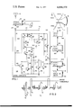
- FIG. 1 is a schematic diagram, partially in block form, of a television receiver embodying the invention.
- FIG. 2 illustrates a waveform at a terminal A in the schematic diagram of FIG. 1.
- an antenna 12 intercepts radio frequency (RF) electromagnetic signals and produces RF electrical signals which are coupled to signal circuits 14.
- the RF signals coupled to signal circuits 14 are amplified and detected to recover the modulation of the video carrier which is representative of the video signal transmitted.
- the recovered video signal is provided at an output terminal 16 and is coupled to the control electrode of the kinescope 18 to provide for intensity modulation of the electron beam produced within the kinescope 18.
- the video signal including synchronizing information is provided at an output terminal 20 of signal circuits 14.
- the detected signal produced by the signal circuits 14 also contains modulation of the audio carrier which is representative of the audio signal transmitted.
- the recovered audio signal is provided at an output terminal 22 which is coupled to a speaker 24 which transforms the audio signals into acoustic waves.
- the video signals including synchronizing signals developed at terminal 20 of signal circuits 14 are coupled through a capacitor 26 to a terminal A of sync circuits 28.
- the operation will be considered under the following conditions: (1) operation during the sync interval (t 0 -t 3 of FIG. 2); and, (2) operation during a noise pulse interval (t 4 -t 5 of FIG. 2) when the noise pulse has an amplitude greater than the noise threshold shown in FIG. 2.
- signals produced at terminal A as shown in FIG. 2 did not contain any noise pulses.
- signals at terminal A produce a current through a series combination of a resistor 30, the base-emitter junction of a first transistor 32 of a noise gate 34 and a resistor 36 coupled between terminal A and reference potential.
- the current through the base-emitter junction produces a current from a source of direct current potential (B+) to which the collector electrode of transistor 32 is coupled.
- the voltage produced at terminal A during the interval t 1 -t 2 produces current flow through the series combination of a resistor 44, the base-emitter junction of transistor 46, the parallel combination of a resistor 48 and the base-emitter junction of a transistor 50 and the collector-emitter junction of transistor 40 to reference potential.
- Current flow through the base-emitter junctions of transistors 46 and 50 provides for current flow through the collector-emitter junction of transistor 46 from the current source 52 comprising transistors 54, 56 and 58, diode 60 and resistor 62.
- Forward biasing of the base-emitter junction of transistor 50 provides for current flow through diodes 64 and 66 coupled in series combination between the current source 52 and the collector electrode of transistor 50.
- diodes 64 and 66 With current flowing through diodes 64 and 66, the potential at the junction of the diodes 64 and 66 is below the level which is required to forward bias a diode 68 in series combination with a resistor 70, which series combination is coupled between the junction of diodes 64 and 66 and reference potential. Under this condition, the voltage developed at the junction of diode 68 and the resistor 70 is approximately zero volts; therefore, no current flows through the series combination of a resistor 72, the base-emitter junction of a transistor 74, and a resistor 76 coupled in parallel with resistor 70, or through a resistor 78 and the base-emitter junction of a transistor 80 also coupled in parallel with resistor 70.
- transistor 74 With no current flow through the base-emitter junction of transistor 74, transistor 74 is cut off and a capacitor 82 coupled to the collector electrode of transistor 74 begins to charge from the constant current source provided for by transistor 84 in combination with a resistor 86 operating in conjunction with the constant current source 52. As the charge on the capacitor 82 increases, the base-emitter junction of a transistor 88 having its collector electrode coupled to B+ and its emitter electrode coupled to reference potential by means of a resistor 90 is forward biased and a voltage is developed across the resistor 90 which corresponds to the voltage across the capacitor 82.
- the emitter electrode of transistor 88 is also coupled to an output terminal 92 which is coupled to a vertical sync processor 94 which provides for a synchronizing pulse at an output terminal 96 at a predetermined voltage level at output terminal 92 of sync circuits 28, which level is only attained once each field of the video signal.
- the synchronizing pulses at terminal 96 are coupled to a vertical deflection circuit 98 which develops a current signal, which is properly phased with the signal at terminal A, through vertical deflection windings 100a and 100b which are coupled between an output terminal 102 of vertical deflection circuit 98 and reference potential.
- transistor 80 With no current flowing through the base-emitter junction of transistor 80, transistor 80 is cut off and the voltage at the collector electrode which is coupled to a constant current source comprising a transistor 104 operating in conjunction with the constant current source 52 provides a potential of approximately B+ at an output terminal 106 which is coupled to a horizontal deflection circuit 108.
- the transition from a potential of approximately reference potential to B+ at terminal 106 at t 1 as shown in FIG. 2 provides for proper synchronization of the signals produced at an output terminal 112 of horizontal deflection circuit 108 and synchronizing signals at terminal A of sync circuits 28.
- Current produced through horizontal deflection windings 112a and 112b coupled between output terminal 110 and reference potential and placed in close proximity with the kinescope 18 provide for horizontal deflection of the electron beam produced in the kinescope 18.
- the horizontal deflection circuit 108 also produces pulses at an output terminal 114 which is coupled to a high voltage multiplier and rectifier 116 thereby developing a high voltage direct current potential at an output terminal 118 which is coupled to the ultor electrode of the kinescope 18.
- the high voltage potential on the ultor electrode of the kinescope 18 provides for the desired acceleration of the electron beam produced in the electron gun of the kinescope 18.
- an output signal developed in an output terminal 120 of vertical sync processor 94 is coupled to the base electrode of a transistor 122.
- the signal at output terminal 120 provides for saturation of the transistor 122, thereby clamping the voltage at the collector electrode of transistor 80 to approximately reference potential during the vertical synchronizing interval.
- the voltage at terminal A is less than that which is required to forward bias the base-emitter junctions of transistors 32 and 46 by way of resistors 30 and 44.
- transistor 50 is also cut off and the potential at the junction of diodes 64 and 66 increases to a level which forward biases the diode 68 and produces a potential at the junction of diode 68 and resistor 70 which provides for forward biasing of the base-emitter junctions of transistors 74 and 80.
- capacitor 82 coupled to the collector electrode of transistor 74 is discharged and the potential at output terminal 92 of sync circuits 28 decreases to approximately reference potential.
- the capacitor 26 can discharge via resistor 27 in order to provide for acknowledgment of subsequent synchronizing signals.
- the capacitor 26 without the noise gate 34 would be charged through resistor 44 and the base-emitter junctions of transistor 46 and 50 to an abnormally high voltage. With capacitor 26 charged to the abnormally high voltage, capacitor 26 would normally not be discharged sufficiently at the beginning of the next synchronizing interval such as at t 0 ' to provide for forward biasing of the base-emitter junctions of transistors 46 and 50 by the synchronizing signal occurring between t 0 ' and t 3 '. Therefore, proper synchronization of the vertical and horizontal deflection circuits would not be maintained.
- noise gate 34 which, in conjunction with resistor 30, establishes the noise threshold as shown in FIG. 2, noise pulses produced at terminal A of sync circuits 28 which exceed the noise threshold, develop a voltage across resistor 36 which provides for forward biasing of the base-emitter junction of transistor 38, thereby reducing the voltage at the collector electrode of transistor 38 to a level which provides for cutoff of the transistor 40.
- the impedance looking into the base-emitter junction of transistor 46 is very high and, therefore, the charging impedance for capacitor 26 is the resistance of resistor 30 plus the input impedance of transistor 32.
- the charging rate of capacitor 26 is increased by approximately the ratio of resistance of resistor 30 to the resistance of resistor 44. This technique minimizes the change of charge on capacitor 26 during the noise pulse interval.
- the ability of the synchronizing circuits to acknowledge synchronizing signals occurring subsequent to noise pulses is greatly enhanced by the use of the noise gate.
Landscapes
- Engineering & Computer Science (AREA)
- Multimedia (AREA)
- Signal Processing (AREA)
- Details Of Television Scanning (AREA)
- Synchronizing For Television (AREA)
- Picture Signal Circuits (AREA)
- Amplifiers (AREA)
Applications Claiming Priority (2)
| Application Number | Priority Date | Filing Date | Title |
|---|---|---|---|
| GB37881/75A GB1525256A (en) | 1975-09-15 | 1975-09-15 | Synchronizing signal separator having an automatic noise gate |
| UK37881/75 | 1975-09-15 |
Publications (1)
| Publication Number | Publication Date |
|---|---|
| US4008370A true US4008370A (en) | 1977-02-15 |
Family
ID=10399670
Family Applications (1)
| Application Number | Title | Priority Date | Filing Date |
|---|---|---|---|
| US05/649,973 Expired - Lifetime US4008370A (en) | 1975-09-15 | 1976-01-19 | Automatic noise gate for a synchronizing signal amplifier |
Country Status (12)
| Country | Link |
|---|---|
| US (1) | US4008370A (cg-RX-API-DMAC10.html) |
| JP (1) | JPS5236415A (cg-RX-API-DMAC10.html) |
| AT (1) | ATA670176A (cg-RX-API-DMAC10.html) |
| AU (1) | AU508222B2 (cg-RX-API-DMAC10.html) |
| BE (1) | BE846191A (cg-RX-API-DMAC10.html) |
| DE (1) | DE2641298C3 (cg-RX-API-DMAC10.html) |
| ES (1) | ES451537A1 (cg-RX-API-DMAC10.html) |
| FR (1) | FR2324177A1 (cg-RX-API-DMAC10.html) |
| GB (1) | GB1525256A (cg-RX-API-DMAC10.html) |
| IT (1) | IT1068499B (cg-RX-API-DMAC10.html) |
| NL (1) | NL7610198A (cg-RX-API-DMAC10.html) |
| SE (1) | SE415315B (cg-RX-API-DMAC10.html) |
Citations (2)
| Publication number | Priority date | Publication date | Assignee | Title |
|---|---|---|---|---|
| US3441669A (en) * | 1965-02-26 | 1969-04-29 | Rca Corp | Threshold control for sync separator noise protection circuit and for agc stage |
| US3639780A (en) * | 1968-06-24 | 1972-02-01 | Gte Sylvania Inc | Video signalling processing apparatus |
Family Cites Families (3)
| Publication number | Priority date | Publication date | Assignee | Title |
|---|---|---|---|---|
| NL97482C (cg-RX-API-DMAC10.html) * | 1957-07-10 | |||
| US3234328A (en) * | 1963-03-01 | 1966-02-08 | Motorola Inc | Television receiver |
| US3256502A (en) * | 1964-02-28 | 1966-06-14 | Sylvania Electric Prod | Sync pulse separating and agc circuitry |
-
1975
- 1975-09-15 GB GB37881/75A patent/GB1525256A/en not_active Expired
-
1976
- 1976-01-19 US US05/649,973 patent/US4008370A/en not_active Expired - Lifetime
- 1976-09-03 SE SE7609789A patent/SE415315B/xx unknown
- 1976-09-09 AU AU17565/76A patent/AU508222B2/en not_active Expired
- 1976-09-09 IT IT27039/76A patent/IT1068499B/it active
- 1976-09-10 AT AT670176A patent/ATA670176A/de not_active Application Discontinuation
- 1976-09-13 JP JP51110687A patent/JPS5236415A/ja active Granted
- 1976-09-14 BE BE170630A patent/BE846191A/xx unknown
- 1976-09-14 FR FR7627579A patent/FR2324177A1/fr not_active Withdrawn
- 1976-09-14 NL NL7610198A patent/NL7610198A/xx not_active Application Discontinuation
- 1976-09-14 DE DE2641298A patent/DE2641298C3/de not_active Expired
- 1976-09-15 ES ES451537A patent/ES451537A1/es not_active Expired
Patent Citations (2)
| Publication number | Priority date | Publication date | Assignee | Title |
|---|---|---|---|---|
| US3441669A (en) * | 1965-02-26 | 1969-04-29 | Rca Corp | Threshold control for sync separator noise protection circuit and for agc stage |
| US3639780A (en) * | 1968-06-24 | 1972-02-01 | Gte Sylvania Inc | Video signalling processing apparatus |
Also Published As
| Publication number | Publication date |
|---|---|
| DE2641298A1 (de) | 1977-03-17 |
| GB1525256A (en) | 1978-09-20 |
| DE2641298C3 (de) | 1979-03-22 |
| AU508222B2 (en) | 1980-03-13 |
| ES451537A1 (es) | 1977-12-01 |
| DE2641298B2 (de) | 1977-10-27 |
| BE846191A (fr) | 1976-12-31 |
| FR2324177A1 (fr) | 1977-04-08 |
| SE7609789L (sv) | 1977-03-16 |
| AU1756576A (en) | 1978-03-16 |
| SE415315B (sv) | 1980-09-22 |
| NL7610198A (nl) | 1977-03-17 |
| JPS5519111B2 (cg-RX-API-DMAC10.html) | 1980-05-23 |
| IT1068499B (it) | 1985-03-21 |
| ATA670176A (de) | 1980-11-15 |
| JPS5236415A (en) | 1977-03-19 |
Similar Documents
| Publication | Publication Date | Title |
|---|---|---|
| US3919482A (en) | FM receiver noise suppression circuit | |
| US4115812A (en) | Automatic gain control circuit | |
| US4013964A (en) | Automatic gain control means for a single sideband radio receiver | |
| US4032973A (en) | Positive feedback high gain agc amplifier | |
| US3441669A (en) | Threshold control for sync separator noise protection circuit and for agc stage | |
| US4212032A (en) | Synchronization and gain control circuit | |
| US2906817A (en) | Television receiver signal processing circuits | |
| US4042959A (en) | Noise suppression circuit | |
| US3450834A (en) | Automatic gain control circuit | |
| US2736769A (en) | Noise cut-off synchronizing signal separator | |
| US4172239A (en) | Signal attenuator | |
| US3454721A (en) | Transistorized agc system | |
| US2956118A (en) | Selective amplitude discriminatory circuit | |
| US4216502A (en) | Peak detector circuit | |
| US4008370A (en) | Automatic noise gate for a synchronizing signal amplifier | |
| US3700803A (en) | Self-tracking noise suppressing circuit | |
| US3512040A (en) | Television receiver deflection circuit using a controlled rectifier | |
| US3555182A (en) | Plural operating mode automatic gain control system | |
| US4218708A (en) | Keyed AGC circuit | |
| US3976836A (en) | Automatic black level setting circuit | |
| US3109061A (en) | Noise cut-off agc and sync-separator tubes | |
| US3165699A (en) | Automatic gain control system for suppressed carrier single sideband radio receivers | |
| US2797258A (en) | Sync separator | |
| US3548097A (en) | Transistorized control circuitry for television receiver | |
| US3126514A (en) | John w |
Legal Events
| Date | Code | Title | Description |
|---|---|---|---|
| AS | Assignment |
Owner name: RCA LICENSING CORPORATION, TWO INDEPENDENCE WAY, P Free format text: ASSIGNMENT OF ASSIGNORS INTEREST.;ASSIGNOR:RCA CORPORATION, A CORP. OF DE;REEL/FRAME:004993/0131 Effective date: 19871208 |