US4008079A - Superconducting alloys - Google Patents
Superconducting alloys Download PDFInfo
- Publication number
- US4008079A US4008079A US05/558,623 US55862375A US4008079A US 4008079 A US4008079 A US 4008079A US 55862375 A US55862375 A US 55862375A US 4008079 A US4008079 A US 4008079A
- Authority
- US
- United States
- Prior art keywords
- alloy
- alloys
- lead
- particles
- matrix
- Prior art date
- Legal status (The legal status is an assumption and is not a legal conclusion. Google has not performed a legal analysis and makes no representation as to the accuracy of the status listed.)
- Expired - Lifetime
Links
- 229910001281 superconducting alloy Inorganic materials 0.000 title abstract 2
- 229910045601 alloy Inorganic materials 0.000 claims abstract description 93
- 239000000956 alloy Substances 0.000 claims abstract description 93
- 239000002245 particle Substances 0.000 claims abstract description 39
- 229910052797 bismuth Inorganic materials 0.000 claims abstract description 34
- 239000010949 copper Substances 0.000 claims abstract description 27
- 229910052802 copper Inorganic materials 0.000 claims abstract description 26
- 239000011159 matrix material Substances 0.000 claims abstract description 21
- RYGMFSIKBFXOCR-UHFFFAOYSA-N Copper Chemical compound [Cu] RYGMFSIKBFXOCR-UHFFFAOYSA-N 0.000 claims abstract description 16
- PXHVJJICTQNCMI-UHFFFAOYSA-N Nickel Chemical compound [Ni] PXHVJJICTQNCMI-UHFFFAOYSA-N 0.000 claims abstract description 16
- JCXGWMGPZLAOME-UHFFFAOYSA-N bismuth atom Chemical compound [Bi] JCXGWMGPZLAOME-UHFFFAOYSA-N 0.000 claims abstract description 12
- 239000011669 selenium Substances 0.000 claims abstract description 10
- 150000001875 compounds Chemical class 0.000 claims abstract description 8
- 229910052738 indium Inorganic materials 0.000 claims abstract description 8
- APFVFJFRJDLVQX-UHFFFAOYSA-N indium atom Chemical compound [In] APFVFJFRJDLVQX-UHFFFAOYSA-N 0.000 claims abstract description 8
- 229910052759 nickel Inorganic materials 0.000 claims abstract description 8
- 229910052711 selenium Inorganic materials 0.000 claims abstract description 7
- 229910052714 tellurium Inorganic materials 0.000 claims abstract description 7
- BUGBHKTXTAQXES-UHFFFAOYSA-N Selenium Chemical compound [Se] BUGBHKTXTAQXES-UHFFFAOYSA-N 0.000 claims abstract description 6
- PORWMNRCUJJQNO-UHFFFAOYSA-N tellurium atom Chemical compound [Te] PORWMNRCUJJQNO-UHFFFAOYSA-N 0.000 claims abstract description 6
- 239000011575 calcium Substances 0.000 claims abstract description 5
- VYZAMTAEIAYCRO-UHFFFAOYSA-N Chromium Chemical compound [Cr] VYZAMTAEIAYCRO-UHFFFAOYSA-N 0.000 claims abstract description 4
- 229910052804 chromium Inorganic materials 0.000 claims abstract description 4
- 239000011651 chromium Substances 0.000 claims abstract description 4
- OYPRJOBELJOOCE-UHFFFAOYSA-N Calcium Chemical compound [Ca] OYPRJOBELJOOCE-UHFFFAOYSA-N 0.000 claims abstract description 3
- 229910052684 Cerium Inorganic materials 0.000 claims abstract description 3
- 229910052791 calcium Inorganic materials 0.000 claims abstract description 3
- ZMIGMASIKSOYAM-UHFFFAOYSA-N cerium Chemical compound [Ce][Ce][Ce][Ce][Ce][Ce][Ce][Ce][Ce][Ce][Ce][Ce][Ce][Ce][Ce][Ce][Ce][Ce][Ce][Ce][Ce][Ce][Ce][Ce][Ce][Ce][Ce][Ce][Ce][Ce][Ce][Ce][Ce][Ce][Ce][Ce][Ce][Ce] ZMIGMASIKSOYAM-UHFFFAOYSA-N 0.000 claims abstract description 3
- 229910052732 germanium Inorganic materials 0.000 claims abstract description 3
- GNPVGFCGXDBREM-UHFFFAOYSA-N germanium atom Chemical compound [Ge] GNPVGFCGXDBREM-UHFFFAOYSA-N 0.000 claims abstract description 3
- 229910052746 lanthanum Inorganic materials 0.000 claims abstract description 3
- FZLIPJUXYLNCLC-UHFFFAOYSA-N lanthanum atom Chemical compound [La] FZLIPJUXYLNCLC-UHFFFAOYSA-N 0.000 claims abstract description 3
- WPBNNNQJVZRUHP-UHFFFAOYSA-L manganese(2+);methyl n-[[2-(methoxycarbonylcarbamothioylamino)phenyl]carbamothioyl]carbamate;n-[2-(sulfidocarbothioylamino)ethyl]carbamodithioate Chemical compound [Mn+2].[S-]C(=S)NCCNC([S-])=S.COC(=O)NC(=S)NC1=CC=CC=C1NC(=S)NC(=O)OC WPBNNNQJVZRUHP-UHFFFAOYSA-L 0.000 claims abstract description 3
- 239000000463 material Substances 0.000 claims description 27
- 239000002887 superconductor Substances 0.000 claims description 10
- 239000008240 homogeneous mixture Substances 0.000 claims description 6
- YBNMDCCMCLUHBL-UHFFFAOYSA-N (2,5-dioxopyrrolidin-1-yl) 4-pyren-1-ylbutanoate Chemical compound C=1C=C(C2=C34)C=CC3=CC=CC4=CC=C2C=1CCCC(=O)ON1C(=O)CCC1=O YBNMDCCMCLUHBL-UHFFFAOYSA-N 0.000 claims description 3
- 229910002665 PbTe Inorganic materials 0.000 claims description 3
- OCGWQDWYSQAFTO-UHFFFAOYSA-N tellanylidenelead Chemical compound [Pb]=[Te] OCGWQDWYSQAFTO-UHFFFAOYSA-N 0.000 claims description 3
- 229910016272 Bi2 Te3 Inorganic materials 0.000 claims 1
- 238000005266 casting Methods 0.000 abstract description 21
- 239000006185 dispersion Substances 0.000 abstract description 6
- 239000000470 constituent Substances 0.000 abstract description 2
- 238000001816 cooling Methods 0.000 description 22
- 238000000034 method Methods 0.000 description 12
- 239000000203 mixture Substances 0.000 description 11
- 238000002844 melting Methods 0.000 description 8
- 230000008018 melting Effects 0.000 description 8
- 239000000243 solution Substances 0.000 description 8
- 229910000978 Pb alloy Inorganic materials 0.000 description 7
- 239000000654 additive Substances 0.000 description 7
- 230000005291 magnetic effect Effects 0.000 description 7
- 238000001556 precipitation Methods 0.000 description 7
- 238000012360 testing method Methods 0.000 description 7
- 230000006872 improvement Effects 0.000 description 6
- 239000011572 manganese Substances 0.000 description 6
- 239000000155 melt Substances 0.000 description 6
- 230000000996 additive effect Effects 0.000 description 5
- 229910052751 metal Inorganic materials 0.000 description 5
- 239000002184 metal Substances 0.000 description 5
- 238000007792 addition Methods 0.000 description 4
- 229910052745 lead Inorganic materials 0.000 description 4
- 239000007788 liquid Substances 0.000 description 4
- 238000005275 alloying Methods 0.000 description 3
- 230000008901 benefit Effects 0.000 description 3
- 230000015572 biosynthetic process Effects 0.000 description 3
- 239000010419 fine particle Substances 0.000 description 3
- 230000004907 flux Effects 0.000 description 3
- 238000007710 freezing Methods 0.000 description 3
- 230000008014 freezing Effects 0.000 description 3
- 238000004519 manufacturing process Methods 0.000 description 3
- IJGRMHOSHXDMSA-UHFFFAOYSA-N Atomic nitrogen Chemical compound N#N IJGRMHOSHXDMSA-UHFFFAOYSA-N 0.000 description 2
- 229910001152 Bi alloy Inorganic materials 0.000 description 2
- OKTJSMMVPCPJKN-UHFFFAOYSA-N Carbon Chemical compound [C] OKTJSMMVPCPJKN-UHFFFAOYSA-N 0.000 description 2
- CURLTUGMZLYLDI-UHFFFAOYSA-N Carbon dioxide Chemical compound O=C=O CURLTUGMZLYLDI-UHFFFAOYSA-N 0.000 description 2
- DGAQECJNVWCQMB-PUAWFVPOSA-M Ilexoside XXIX Chemical compound C[C@@H]1CC[C@@]2(CC[C@@]3(C(=CC[C@H]4[C@]3(CC[C@@H]5[C@@]4(CC[C@@H](C5(C)C)OS(=O)(=O)[O-])C)C)[C@@H]2[C@]1(C)O)C)C(=O)O[C@H]6[C@@H]([C@H]([C@@H]([C@H](O6)CO)O)O)O.[Na+] DGAQECJNVWCQMB-PUAWFVPOSA-M 0.000 description 2
- PWHULOQIROXLJO-UHFFFAOYSA-N Manganese Chemical compound [Mn] PWHULOQIROXLJO-UHFFFAOYSA-N 0.000 description 2
- 230000005540 biological transmission Effects 0.000 description 2
- 239000004020 conductor Substances 0.000 description 2
- 238000011161 development Methods 0.000 description 2
- 230000018109 developmental process Effects 0.000 description 2
- 229910002804 graphite Inorganic materials 0.000 description 2
- 239000010439 graphite Substances 0.000 description 2
- 229910052748 manganese Inorganic materials 0.000 description 2
- 150000002739 metals Chemical class 0.000 description 2
- 230000003647 oxidation Effects 0.000 description 2
- 238000007254 oxidation reaction Methods 0.000 description 2
- 239000002244 precipitate Substances 0.000 description 2
- 230000002028 premature Effects 0.000 description 2
- 230000008569 process Effects 0.000 description 2
- 239000000047 product Substances 0.000 description 2
- 238000010791 quenching Methods 0.000 description 2
- 230000000171 quenching effect Effects 0.000 description 2
- 230000009467 reduction Effects 0.000 description 2
- 238000001878 scanning electron micrograph Methods 0.000 description 2
- 229910052708 sodium Inorganic materials 0.000 description 2
- 239000011734 sodium Substances 0.000 description 2
- 239000007787 solid Substances 0.000 description 2
- 229910052716 thallium Inorganic materials 0.000 description 2
- BKVIYDNLLOSFOA-UHFFFAOYSA-N thallium Chemical compound [Tl] BKVIYDNLLOSFOA-UHFFFAOYSA-N 0.000 description 2
- XLYOFNOQVPJJNP-UHFFFAOYSA-N water Substances O XLYOFNOQVPJJNP-UHFFFAOYSA-N 0.000 description 2
- 229910000881 Cu alloy Inorganic materials 0.000 description 1
- 229910000528 Na alloy Inorganic materials 0.000 description 1
- 229910001257 Nb alloy Inorganic materials 0.000 description 1
- 229910001275 Niobium-titanium Inorganic materials 0.000 description 1
- 229910000831 Steel Inorganic materials 0.000 description 1
- 230000002378 acidificating effect Effects 0.000 description 1
- 230000009471 action Effects 0.000 description 1
- 238000004458 analytical method Methods 0.000 description 1
- 230000005290 antiferromagnetic effect Effects 0.000 description 1
- QVGXLLKOCUKJST-UHFFFAOYSA-N atomic oxygen Chemical compound [O] QVGXLLKOCUKJST-UHFFFAOYSA-N 0.000 description 1
- 230000009286 beneficial effect Effects 0.000 description 1
- 229910000675 bismuth manganese alloy Inorganic materials 0.000 description 1
- 238000009835 boiling Methods 0.000 description 1
- 229910002092 carbon dioxide Inorganic materials 0.000 description 1
- 239000001569 carbon dioxide Substances 0.000 description 1
- 150000004649 carbonic acid derivatives Chemical class 0.000 description 1
- 230000008859 change Effects 0.000 description 1
- 239000004927 clay Substances 0.000 description 1
- 238000011109 contamination Methods 0.000 description 1
- 238000000354 decomposition reaction Methods 0.000 description 1
- 230000002939 deleterious effect Effects 0.000 description 1
- 230000003467 diminishing effect Effects 0.000 description 1
- 230000000694 effects Effects 0.000 description 1
- 238000010894 electron beam technology Methods 0.000 description 1
- 230000008030 elimination Effects 0.000 description 1
- 238000003379 elimination reaction Methods 0.000 description 1
- 238000005516 engineering process Methods 0.000 description 1
- 238000002474 experimental method Methods 0.000 description 1
- 239000007789 gas Substances 0.000 description 1
- 238000007429 general method Methods 0.000 description 1
- 239000001307 helium Substances 0.000 description 1
- 229910052734 helium Inorganic materials 0.000 description 1
- SWQJXJOGLNCZEY-UHFFFAOYSA-N helium atom Chemical compound [He] SWQJXJOGLNCZEY-UHFFFAOYSA-N 0.000 description 1
- 239000001257 hydrogen Substances 0.000 description 1
- 229910052739 hydrogen Inorganic materials 0.000 description 1
- 150000004679 hydroxides Chemical class 0.000 description 1
- 230000003116 impacting effect Effects 0.000 description 1
- 238000011031 large-scale manufacturing process Methods 0.000 description 1
- 229910000464 lead oxide Inorganic materials 0.000 description 1
- 230000005415 magnetization Effects 0.000 description 1
- 229910052758 niobium Inorganic materials 0.000 description 1
- 239000010955 niobium Substances 0.000 description 1
- GUCVJGMIXFAOAE-UHFFFAOYSA-N niobium atom Chemical compound [Nb] GUCVJGMIXFAOAE-UHFFFAOYSA-N 0.000 description 1
- KJSMVPYGGLPWOE-UHFFFAOYSA-N niobium tin Chemical compound [Nb].[Sn] KJSMVPYGGLPWOE-UHFFFAOYSA-N 0.000 description 1
- RJSRQTFBFAJJIL-UHFFFAOYSA-N niobium titanium Chemical compound [Ti].[Nb] RJSRQTFBFAJJIL-UHFFFAOYSA-N 0.000 description 1
- 229910000657 niobium-tin Inorganic materials 0.000 description 1
- 229910052757 nitrogen Inorganic materials 0.000 description 1
- 230000010355 oscillation Effects 0.000 description 1
- YEXPOXQUZXUXJW-UHFFFAOYSA-N oxolead Chemical compound [Pb]=O YEXPOXQUZXUXJW-UHFFFAOYSA-N 0.000 description 1
- 239000001301 oxygen Substances 0.000 description 1
- 229910052760 oxygen Inorganic materials 0.000 description 1
- 230000005298 paramagnetic effect Effects 0.000 description 1
- 238000004663 powder metallurgy Methods 0.000 description 1
- 230000001376 precipitating effect Effects 0.000 description 1
- 238000002360 preparation method Methods 0.000 description 1
- 238000005096 rolling process Methods 0.000 description 1
- 230000035945 sensitivity Effects 0.000 description 1
- 238000005476 soldering Methods 0.000 description 1
- 239000006104 solid solution Substances 0.000 description 1
- 238000005507 spraying Methods 0.000 description 1
- 239000010935 stainless steel Substances 0.000 description 1
- 229910001220 stainless steel Inorganic materials 0.000 description 1
- 239000010959 steel Substances 0.000 description 1
- 238000003878 thermal aging Methods 0.000 description 1
- 231100000925 very toxic Toxicity 0.000 description 1
- 238000003466 welding Methods 0.000 description 1
- 238000004804 winding Methods 0.000 description 1
Images
Classifications
-
- H—ELECTRICITY
- H10—SEMICONDUCTOR DEVICES; ELECTRIC SOLID-STATE DEVICES NOT OTHERWISE PROVIDED FOR
- H10N—ELECTRIC SOLID-STATE DEVICES NOT OTHERWISE PROVIDED FOR
- H10N60/00—Superconducting devices
- H10N60/80—Constructional details
- H10N60/85—Superconducting active materials
-
- Y—GENERAL TAGGING OF NEW TECHNOLOGICAL DEVELOPMENTS; GENERAL TAGGING OF CROSS-SECTIONAL TECHNOLOGIES SPANNING OVER SEVERAL SECTIONS OF THE IPC; TECHNICAL SUBJECTS COVERED BY FORMER USPC CROSS-REFERENCE ART COLLECTIONS [XRACs] AND DIGESTS
- Y10—TECHNICAL SUBJECTS COVERED BY FORMER USPC
- Y10S—TECHNICAL SUBJECTS COVERED BY FORMER USPC CROSS-REFERENCE ART COLLECTIONS [XRACs] AND DIGESTS
- Y10S420/00—Alloys or metallic compositions
- Y10S420/901—Superconductive
-
- Y—GENERAL TAGGING OF NEW TECHNOLOGICAL DEVELOPMENTS; GENERAL TAGGING OF CROSS-SECTIONAL TECHNOLOGIES SPANNING OVER SEVERAL SECTIONS OF THE IPC; TECHNICAL SUBJECTS COVERED BY FORMER USPC CROSS-REFERENCE ART COLLECTIONS [XRACs] AND DIGESTS
- Y10—TECHNICAL SUBJECTS COVERED BY FORMER USPC
- Y10S—TECHNICAL SUBJECTS COVERED BY FORMER USPC CROSS-REFERENCE ART COLLECTIONS [XRACs] AND DIGESTS
- Y10S505/00—Superconductor technology: apparatus, material, process
- Y10S505/80—Material per se process of making same
- Y10S505/801—Composition
- Y10S505/805—Alloy or metallic
-
- Y—GENERAL TAGGING OF NEW TECHNOLOGICAL DEVELOPMENTS; GENERAL TAGGING OF CROSS-SECTIONAL TECHNOLOGIES SPANNING OVER SEVERAL SECTIONS OF THE IPC; TECHNICAL SUBJECTS COVERED BY FORMER USPC CROSS-REFERENCE ART COLLECTIONS [XRACs] AND DIGESTS
- Y10—TECHNICAL SUBJECTS COVERED BY FORMER USPC
- Y10S—TECHNICAL SUBJECTS COVERED BY FORMER USPC CROSS-REFERENCE ART COLLECTIONS [XRACs] AND DIGESTS
- Y10S505/00—Superconductor technology: apparatus, material, process
- Y10S505/80—Material per se process of making same
- Y10S505/812—Stock
- Y10S505/813—Wire, tape, or film
-
- Y—GENERAL TAGGING OF NEW TECHNOLOGICAL DEVELOPMENTS; GENERAL TAGGING OF CROSS-SECTIONAL TECHNOLOGIES SPANNING OVER SEVERAL SECTIONS OF THE IPC; TECHNICAL SUBJECTS COVERED BY FORMER USPC CROSS-REFERENCE ART COLLECTIONS [XRACs] AND DIGESTS
- Y10—TECHNICAL SUBJECTS COVERED BY FORMER USPC
- Y10S—TECHNICAL SUBJECTS COVERED BY FORMER USPC CROSS-REFERENCE ART COLLECTIONS [XRACs] AND DIGESTS
- Y10S505/00—Superconductor technology: apparatus, material, process
- Y10S505/825—Apparatus per se, device per se, or process of making or operating same
- Y10S505/911—Fluid reaction surface, i.e. impeller
-
- Y—GENERAL TAGGING OF NEW TECHNOLOGICAL DEVELOPMENTS; GENERAL TAGGING OF CROSS-SECTIONAL TECHNOLOGIES SPANNING OVER SEVERAL SECTIONS OF THE IPC; TECHNICAL SUBJECTS COVERED BY FORMER USPC CROSS-REFERENCE ART COLLECTIONS [XRACs] AND DIGESTS
- Y10—TECHNICAL SUBJECTS COVERED BY FORMER USPC
- Y10S—TECHNICAL SUBJECTS COVERED BY FORMER USPC CROSS-REFERENCE ART COLLECTIONS [XRACs] AND DIGESTS
- Y10S505/00—Superconductor technology: apparatus, material, process
- Y10S505/825—Apparatus per se, device per se, or process of making or operating same
- Y10S505/912—Metal founding
- Y10S505/913—Casting process
- Y10S505/915—Making composite product
Definitions
- the present invention relates to Type II superconducors and in particular to Type II superconductors having high critical currents.
- Niobium metal is itself very expensive and the techniques of working the alloy to produce a suitable conductor are both difficult and expensive.
- the cost of niobium alloy, in the form of a suitable conductor, is a significant aspect of the capital cost of a superconducting cable system using it.
- Attempts have been made to find other suitable alloys.
- One such attempt is described in British Patent Specification No. 1137427. This specification describes a system of alloys based on lead and incorporating a dispersion of fine particles of oxides of the lead and/or other alloying component. The alloys produced have improved (upper) critical currents at moderate applied fields.
- ⁇ critical ⁇ parameters of Type II superconductors is to be understood as being to ⁇ upper critical ⁇ parameters.
- the applied fields are usually fairly low, less than 5 kG and the critical field is not likely to be a limiting factor for systems having at least moderately high critical temperatures.
- the alloys described in this prior specification suffer from certain disadvantages in that the oxides produced tend to combine chemically with water or carbon dioxide to produce thermally unstable hydroxides or carbonates. Decomposition of such materials incorporated in the alloy can cause blistering if the alloy is heat-processed e.g., by extruding at high temperatures or soldering or welding.
- the process used for preparing the oxide dispersion gives a non-uniform dispersion of coarse oxide particles. These problems can be overcome but at the expense of increased cost of manufacture. Further, the oxide dispersion reduces the ductility of the alloy and at high levels of oxide, which are advantageous from the improvement in superconducting properties, the reduction in ductility can be so marked as to make working of the alloys difficult.
- the particles of oxide dispersed in the alloy act as pinning centres for Abrikosov flux vortices thus allowing much higher values of critical current to be attained than in the unmodified alloy.
- the present invention is directed to an alternative way of providing pinning centres and in particular to providing smaller and more closely spaced pinning centres.
- the present invention provides an alloy comprising a matrix of a Type II superconductor, which is an homogeneous mixture of lead with bismuth and/or indium, including, dispersed in the matrix, a material to provide pinning centres comprising at least 0.01% by volume of a stable discontinuous phase comprising discrete crystalline particles of copper, manganese, tellurium, selenium, nickel, calcium, chromium, cerium, germanium or lanthanum either in the form of the element or of a compound with at least one of the components of the matrix, wherein the discrete particles have an average diameter of not more than 2 microns, preferably not more than 0.5 microns.
- Type II superconductors of the present type by using thallium or sodium as the other constituent of the lead based alloy, however, these materials are not as useful as alloys using indium and/or bismuth. Further thallium is very toxic and sodium produces chemically reactive alloys which may not be stable in an operational environment.
- a second aspect of the invention provides an alloy comprising a matrix of a Type II superconductor including, dispersed in the matrix, a material to provide pinning centres comprising at least 0.01% by volume of a stable discontinuous phase in the form of discrete particles having an average diameter of not more than 2 microns and formed by cooling an homogeneous liquid mixture of the alloy components at an average cooling rate of at least 10 3 ° C. sec - 1 , preferably more than 10 5 ° C. sec - 1 , to a temperature at which the alloy is substantially completely solid.
- the invention also provides superconducting elements made from or comprising the alloy of the invention at a temperature below its critical temperature.
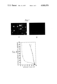
- FIG. 1 (a and b) shows scanning electron micrographs of an alloy of the invention.
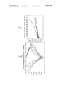
- FIGS. 2 (a, b, and c) and 5 show plots of magnetization versus applied magnetic field for various alloys of the invention.
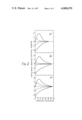
- FIGS. 3 and 4 are plots of critical current density versus applied magnetic field for alloys of the invention.
- cryogenic systems are operated at or about 4.2° K because this is the normal boiling point of liquid helium and can therefore be maintained fairly straight-forwardly. It is thus preferred to use alloys having critical temperatures somewhat in excess of this figure in order to obtain practically useful values of critical current at operational magnetic fields.
- the composition of the alloys are limited in respect of the proportion of X to a minimum figure at least sufficient that the alloy is a Type II superconductor.
- the preferred upper figure is limited by the phase stability of the material.
- the matrix alloys used in the invention should contain a minimum of 50% of lead and a minimum of 5% of bismuth or 10% of indium. The following are preferred practical ranges for the amount of X in atom percent based on the total alloy:
- the particles forming the discontinuous phase are of a material which is insoluble in the solid matrix.
- the precise composition of the discontinuous phase in any particular instance will thus depend to some extent on the composition of the matrix.
- the products of the invention are made in the first instance by freezing an homogeneous molten solution of the basic components of the alloy at a cooling rate of at least 10 3 ° C. sec - 1 , preferably at least 10 5 ° C. sec - 1 , thus precipitating the discontinuous phase in the form of particles having an average diameter of not more than 2 microns, preferably less than this, e.g. 0.5 microns, and optimally not more than 0.1 microns. Since particle size is a function of cooling rate and the latter is determined by the freezing technique used, particle size will be discussed later in connection with the different techniques.
- the method of providing the discontinuous phase is to incorporate in solution in the molten base alloy e.g.
- Pb/35% Bi a proportion of a material which will, on cooling, either itself precipitate out of solution as discrete particles or combine with one or more of the components of the basic alloy to precipitate at least one type of discontinuous phase on cooling.
- the phases formed may depend on cooling rate as well as on the composition of the alloy as, at the high cooling rates employed, metastable phases may form.
- Typical additive materials and the phases likely to be precipitated are listed in Table I in relation to the alloying components of the lead alloys mentioned above. As these ternary systems have not been fully investigated there may be other binary and ternary compounds precipitated in addition to those listed.
- the discontinuous phase does not have significant para-, ferro-, or antiferromagnetic properties at superconducting temperatures. Possession of such magnetic properties would have a deleterious effect on the ability of the particles to act as pinning centres.
- manganese can provide pinning centres, it is less effective than might otherwise be expected because it tends to be precipitated in the form of paramagnetic compounds.
- the particles are not of a material which, itself, is a superconductor under operating conditions. It is thought possible that the phase discontinuity might itself act as a pinning centre, but this would be expected to be weaker than the pinning action of a non-superconducting particle under the same conditions.
- disperse phase forming materials used in the invention copper and especially nickel, selenium and tellurium are preferred.
- the amount of material forming the discontinuous phase added to the molten base alloy is preferably sufficient to produce between 0.01 and 20% by volume of discontinuous phase.
- the amount added will be in this range after allowing for density differences and thermal expansion effects.
- the volume of precipitate required is achieved with a lower atomic % of additive, depending on the stoichiometry of the compound formed. The lower limit is determined by practical considerations of providing a significant improvement in superconductive properties.
- the upper level of discontinuous phase is limited by diminishing returns, in terms of improvement of critical current for increased additions and by difficulties associated with solubility in the molten state and the tendency at higher concentrations to form larger particles unless very high cooling rates are employed.
- the general method used to produce the alloys of the invention is by rapid quenching of a molten solution of the appropriate additive in the basic alloy.
- the cooling rate In order to prevent the formation of relatively large particles of disperse phase the cooling rate must be at least 10 3 ° C. sec - 1 .
- sec - 1 represents very nearly the maximum rate of cooling attainable using chill casting and this rate tends to produce relatively coarse dispersions typically in the range of 1 to 2 microns average diameter a significant proportion of particles being up to 10 microns in diameter. These are not very preferred alloys of the invention.
- a liquid to be quenched is atomised and sprayed on to a cooled surface, usually the outer surface of an internally cooled cylinder.
- a cooled surface usually the outer surface of an internally cooled cylinder.
- the atomised droplets of liquid spread out and are rapidly cooled to form a flake.
- Cooling rates of greater than 10 7 ° C. sec - 1 are possible, but in practice cooling rates much in excess of 10 6 ° C. sec - 1 are difficult to maintain in large-scale production.
- the practical limit on the rate of cooling is not a limit on the concept of the invention, merely on the techniques at present available to carry it out. Development of techniques giving even higher rates of cooling will enable finer particles to be precipitated and are thus included in the broad concept of the present invention.
- the additive which comprises or stimulates disperse phase precipitation should be completely dissolved in the molten alloy before spraying. This may mean forming the solution at a temperature considerably in excess of the melting point of the basic alloy.
- copper is only very slightly soluble (ca. 0.1% by weight) at normal melting temperatures.
- additions of about 1% copper it is advisable to heat the molten alloy to 500° C. above the normal melting point of the basic alloy.
- the maximum temperature for lead alloys is limited by the vapour pressure of lead to not higher than about 1100° C, and preferably not higher than 1000° C. for unsealed apparatus.
- the molten solution In order to prevent premature and thus uncontrolled precipitation it is advisable to heat the molten solution to 50° to 150° C. optimally about 100° C. above the liquidus of the mixture, i.e. the temperature at which the disperse phase forming material is completely in solution in the melt.
- undesirable contamination e.g. by oxidation of the alloy when molten it is advisable to keep the surface of the molten alloy under an inert or reducing atmosphere, e.g. N 2 or 90% N 2 / 10% H 2 .
- Choice of correct melting temperature avoids such premature precipitation.
- the droplets On impact on the cooled surface the droplets splat and are rapidly cooled and freeze.
- the cooled surface is the external surface of an internally cooled drum the system is usually provided with a scraper to dislodge flakes adhering to the surface of the drum.
- the cooled drum is conveniently a water-cooled chromium-plated copper drum, which is rotated to present a continuous fresh cool surface for impact.
- the flake obtained from splat casting can be formed by conventional powder metallurgy techniques.
- the alloy should not be heated to a temperature higher than that at which substantial increase in the particle size of the discontinuous phase occurs. This temperature will depend on the particular system employed in a given case.
- the preferred techniques of the invention involve cooling at such high rates that the product may contain "disperse phase forming material" frozen in (supercooled) solid solution. Thermal aging of such materials can stimulate further and beneficial precipitation of the disperse phase.
- the lead based alloys of and produced by the process of the present invention have critical temperatures typical of superconducting lead alloys i.e. about 7° K.
- the critical fields are not very significantly higher than those of equivalent alloys not including the dispersed phase, i.e. about 10 to 15 kG.
- very marked increases of critical current can be achieved. Improvements by a factor of 10 2 to 10 3 are readily obtained with copper additions of as little as 0.1% by weight in a splat cast alloy.
- Alloys of this invention advantageously have a critical current density at 4.2° K and an applied field of 7 kG, of at least 80 A mm - 2 .
- the alloys are expected to have utility primarily in situations where a high critical current is required in a relatively low applied field, for example in power transmission cables.
- the alloys may also have other uses, for example, in the outer windings of cryogenic motors or magnets.
- Chill castings were produced by melting the alloy components under a 90/10 nitrogen-hydrogen atmosphere using an electrical resistance furnace. The melts were cast into a split graphite mould to produce 12.7 mm. and 6.35 mm diameter rods. The 12.7 mm diameter rods were rolled at room temperature to give 270 mm ⁇ 10 mm ⁇ 0.5 mm specimens which were used for determination of the critical current, the 6.35 mm diameter rods were drawn to 2.3 mm diameter for testing magnetisation. The rate of cooling of the chill castings was assessed to be about 10 2 ° C. sec - 1 .
- Splat cast alloys were produced by melting the alloy components in a clay graphite crucible with a hole in the base through which the melt could be bottom poured. During melting this hole was sealed by a conical plug attached to the end of the steel tube which contained the thermocouple for checking the temperature of the melt. After melting the temperature was raised to at least 100° C. above the estimated liquidus temperature and the melt was stirred vigorously immediately before casting. The atomising and quenching unit was completely enclosed and was purged with nitrogen before casting. The stopper rod was withdrawn and the lead alloy poured through the bottom of the crucible as a stream about 2 mm diameter and fell into the apex of a cone formed by a number of high velocity gas jets.
- Flakes produced this way were compacted to 38 mm diameter billets and extruded at room temperature to 6.35 mm diameter rod.
- the 6.35 mm diameter rod was then drawn at room temperature to give 2.3 mm diameter specimens for magnetisation experiments.
- Critical current specimens were produced by extruding the flake through a rectangular section die, 25 mm ⁇ 3 mm and rolling to produce 0.5 mm thickness strip.
- FIGS. 1a and 1b are Cu K ⁇ scanning electron micrographs of chill cast and splat cast specimens respectively (see further under Example 1).
- the magnetisation of the sample at 4.2° K was measured in a vibrating sample magnetometer.
- a superconducting solenoid was used to produce the test field applied to the sample.
- a pair of sensing coils, wound in opposition, was positioned inside the solenoid and the sample vibrated along the common axis of the solenoid and sensing coils.
- the sensing coils cancelled out unwanted signals due to the change in the field being applied to the samples by the solenoid but sensed an a.c. signal due to the magnetisation of the sample as it oscillated between them.
- This a.c. signal was amplified and detected against a second a.c. signal produced from the vibrator which controlled the oscillation of the sample in a phase sensitive detector to give a d.c.
- the critical field can readily be determined from the X-Y plot.
- the degree of hysteresis in the plotted curve is a measure of the flux pinning in the sample.
- FIGS. 2 and 5 are Examples of such hysteresis curves.
- a ⁇ U ⁇ shaped specimen of the alloy being tested was disposed symmetrically along the axis of a superconducting solenoid, at 4.2° K, such that the maximum field generated by the solenoid was transverse to the specimen.
- the critical current was determined by noting the point at which the voltage across the sample monitored using a sensitive volt-meter (lu V sensitivity) became measurable, it being zero whilst the material is superconducting.
- a plot of critical current against transverse field can be produced. Such a plot gives a measure of the amount of current which, say, a superconducting cable made from the test material would be able to carry in operation.
- This Example illustrates the preparation of alloys according to the invention by chill and splat casting and illustrates the advantage of using splat casting.
- Alloys having matrix composition of Pb/25% Bi, Pb/30% Bi and Pb/40% Bi each alloy having 1% Cu incorporated therein were made by chill casting from 800° C. A portion of the chill cast metal was re-melted and splat cast from 800° C. Samples prepared from the two castings were compared. The results are set out in Table II and in FIGS. 1, 2 and 3.
- H c2 figures given in Table II show that there is no significant difference in upper critical field between the chill and splat cast material but that as expected H c2 increases with increasing Bi content.
- FIG. 1 shows copper K ⁇ X-ray images produced in a scanning electron microscope (magnification ⁇ 750) of the alloy in Table II having a (nominal) composition of Pb/40% Bi/1% Cu.
- FIG. 1 a) is chill cast and FIG. 1 b) splat cast.
- FIG. 1 a) shows that relatively coarse copper particles of up to 10 ⁇ m diameter are present in the chill cast material.
- the copper in the splat cast material, FIG. 1 b) is not present as clearly defined particles and must therefore be present as particles smaller than the diameter of the electron beam (0.5 ⁇ m) giving an average particle size (diameter) well below 0.5 ⁇ m.
- FIGS. 2 a, b and c are plots of specimen magnetisation versus applied magnetic field at 4.2° K for the Pb/25% Bi/1% Cu, Pb/30% Bi/1% Cu and Pb/40% Bi/1% Cu alloys respectively.
- the magnetisation is in units of -4 ⁇ M, kG, the applied field in kG.
- the solid line is the result for splat cast material and the dotted line for chill cast material of the same composition. It is very clear that the degree of hysteresis, and thus the amount of flux pinning is much greater for the splat cast alloy than for the chill cast alloy.
- FIG. 3 is a plot of critical current density against applied magnetic field for the alloy in Table II having a (nominal) composition of Pb/30% Bi/1% Cu at 4.2° K. Curve (i) is the chill and curve (ii) the splat cast material. The improvement in critical current density is very marked.
- This Example illustrates a variety of alloys according to the invention and further illustrates the advantage of splat casting.
- FIG. 5 shows magnetisation data for two of the alloys above and for two alloys not given in Table III. These alloys are:
Landscapes
- Superconductors And Manufacturing Methods Therefor (AREA)
- Superconductor Devices And Manufacturing Methods Thereof (AREA)
- Manufacture Of Alloys Or Alloy Compounds (AREA)
Applications Claiming Priority (2)
| Application Number | Priority Date | Filing Date | Title |
|---|---|---|---|
| UK12492/74 | 1974-03-20 | ||
| GB1249274A GB1458284A (en) | 1974-03-20 | 1974-03-20 | Superconducting alloys |
Publications (1)
| Publication Number | Publication Date |
|---|---|
| US4008079A true US4008079A (en) | 1977-02-15 |
Family
ID=10005605
Family Applications (1)
| Application Number | Title | Priority Date | Filing Date |
|---|---|---|---|
| US05/558,623 Expired - Lifetime US4008079A (en) | 1974-03-20 | 1975-03-17 | Superconducting alloys |
Country Status (11)
| Country | Link |
|---|---|
| US (1) | US4008079A (enExample) |
| JP (1) | JPS50133792A (enExample) |
| BE (1) | BE826946A (enExample) |
| CA (1) | CA1058423A (enExample) |
| DE (1) | DE2511882A1 (enExample) |
| ES (1) | ES435732A1 (enExample) |
| FR (1) | FR2264882B1 (enExample) |
| GB (1) | GB1458284A (enExample) |
| IT (1) | IT1034446B (enExample) |
| NL (1) | NL7503007A (enExample) |
| SE (1) | SE7503162L (enExample) |
Cited By (6)
| Publication number | Priority date | Publication date | Assignee | Title |
|---|---|---|---|---|
| US4253871A (en) * | 1978-07-20 | 1981-03-03 | Compagnie Europeenne D'accumulateurs | Alloys for making electrode supports in lead accumulators |
| US4939032A (en) * | 1987-06-25 | 1990-07-03 | Aluminum Company Of America | Composite materials having improved fracture toughness |
| US5226947A (en) * | 1992-02-17 | 1993-07-13 | Wisconsin Alumni Research Foundation | Niobium-titanium superconductors produced by powder metallurgy having artificial flux pinning centers |
| RU2221889C1 (ru) * | 2001-12-21 | 2004-01-20 | Дочернее государственное предприятие "Институт ядерной физики" Национального ядерного центра Республики Казахстан | Способ синтеза интерметаллических соединений |
| US20060272145A1 (en) * | 2005-03-11 | 2006-12-07 | Alabama Cryogenic Engineering, Inc. | Method of producing superconducting wire and articles produced thereby |
| US20210398714A1 (en) * | 2020-02-21 | 2021-12-23 | John A. Wood | Above room temperature type ii superconductor |
Families Citing this family (6)
| Publication number | Priority date | Publication date | Assignee | Title |
|---|---|---|---|---|
| JP2599387B2 (ja) * | 1987-06-02 | 1997-04-09 | 古河電気工業株式会社 | セラミックス超電導体 |
| JPH0221628A (ja) * | 1987-12-28 | 1990-01-24 | Tanaka Electron Ind Co Ltd | 超電導素子用ボンディングpb合金線及び超電導装置 |
| DE3844114C3 (de) * | 1987-12-28 | 1999-03-18 | Tanaka Electronics Ind | Verwendung eines Kontaktierdrahtes aus einer Bleilegierung in einer Supraleitervorrichtung |
| DE3844879C3 (de) * | 1987-12-28 | 1999-06-24 | Tanaka Electronics Ind | Supraleitervorrichtung mit einem Kontaktierdraht |
| JP2550188B2 (ja) * | 1988-11-25 | 1996-11-06 | 株式会社日立製作所 | 酸化物系高温超電導体と接合方法及びろう材 |
| JPH0585987U (ja) * | 1991-07-25 | 1993-11-19 | 信越ユニット株式会社 | ドアエッジ部材の構造 |
Citations (3)
| Publication number | Priority date | Publication date | Assignee | Title |
|---|---|---|---|---|
| US1681272A (en) * | 1925-11-30 | 1928-08-21 | Yoshikawa Hiroshi | Lead alloy |
| US2325071A (en) * | 1940-11-30 | 1943-07-27 | Indium Corp America | Bearing and like article |
| GB1137427A (en) * | 1966-08-04 | 1968-12-18 | Central Electr Generat Board | Improvements in or relating to superconducting alloys and their manufacture |
-
1974
- 1974-03-20 GB GB1249274A patent/GB1458284A/en not_active Expired
-
1975
- 1975-03-13 NL NL7503007A patent/NL7503007A/xx not_active Application Discontinuation
- 1975-03-17 US US05/558,623 patent/US4008079A/en not_active Expired - Lifetime
- 1975-03-18 DE DE19752511882 patent/DE2511882A1/de active Pending
- 1975-03-18 ES ES435732A patent/ES435732A1/es not_active Expired
- 1975-03-19 FR FR7508541A patent/FR2264882B1/fr not_active Expired
- 1975-03-19 CA CA222,532A patent/CA1058423A/en not_active Expired
- 1975-03-19 SE SE7503162A patent/SE7503162L/xx unknown
- 1975-03-19 JP JP50034253A patent/JPS50133792A/ja active Pending
- 1975-03-20 IT IT7521475A patent/IT1034446B/it active
- 1975-03-20 BE BE7000632A patent/BE826946A/xx unknown
Patent Citations (3)
| Publication number | Priority date | Publication date | Assignee | Title |
|---|---|---|---|---|
| US1681272A (en) * | 1925-11-30 | 1928-08-21 | Yoshikawa Hiroshi | Lead alloy |
| US2325071A (en) * | 1940-11-30 | 1943-07-27 | Indium Corp America | Bearing and like article |
| GB1137427A (en) * | 1966-08-04 | 1968-12-18 | Central Electr Generat Board | Improvements in or relating to superconducting alloys and their manufacture |
Cited By (7)
| Publication number | Priority date | Publication date | Assignee | Title |
|---|---|---|---|---|
| US4253871A (en) * | 1978-07-20 | 1981-03-03 | Compagnie Europeenne D'accumulateurs | Alloys for making electrode supports in lead accumulators |
| US4939032A (en) * | 1987-06-25 | 1990-07-03 | Aluminum Company Of America | Composite materials having improved fracture toughness |
| US5226947A (en) * | 1992-02-17 | 1993-07-13 | Wisconsin Alumni Research Foundation | Niobium-titanium superconductors produced by powder metallurgy having artificial flux pinning centers |
| RU2221889C1 (ru) * | 2001-12-21 | 2004-01-20 | Дочернее государственное предприятие "Институт ядерной физики" Национального ядерного центра Республики Казахстан | Способ синтеза интерметаллических соединений |
| US20060272145A1 (en) * | 2005-03-11 | 2006-12-07 | Alabama Cryogenic Engineering, Inc. | Method of producing superconducting wire and articles produced thereby |
| US20210398714A1 (en) * | 2020-02-21 | 2021-12-23 | John A. Wood | Above room temperature type ii superconductor |
| US11710584B2 (en) * | 2020-02-21 | 2023-07-25 | Taj Quantum | Above room temperature type II superconductor |
Also Published As
| Publication number | Publication date |
|---|---|
| DE2511882A1 (de) | 1975-09-25 |
| AU7896675A (en) | 1976-09-16 |
| IT1034446B (it) | 1979-09-10 |
| NL7503007A (nl) | 1975-09-23 |
| SE7503162L (sv) | 1975-09-22 |
| FR2264882B1 (enExample) | 1980-02-15 |
| JPS50133792A (enExample) | 1975-10-23 |
| ES435732A1 (es) | 1977-04-01 |
| FR2264882A1 (enExample) | 1975-10-17 |
| GB1458284A (en) | 1976-12-15 |
| CA1058423A (en) | 1979-07-17 |
| BE826946A (nl) | 1975-09-22 |
Similar Documents
| Publication | Publication Date | Title |
|---|---|---|
| US4008079A (en) | Superconducting alloys | |
| Munitz et al. | Liquid separation in Cu–Co and Cu–Co–Fe alloys solidified at high cooling rates | |
| Munitz et al. | Supercooling effects in Cu-10 Wt Pct Co alloys solidified at different cooling rates | |
| El-Eskandarany et al. | Rod milling for solid-state formation of Al30Ta70 amorphous alloy powder | |
| Chu et al. | Solidification of highly undercooled Sn-Pb alloy droplets | |
| DE69115394T2 (de) | Hochfeste Legierungen auf Aluminiumbasis | |
| US3947265A (en) | Process of adding alloy ingredients to molten metal | |
| McMasters et al. | Preparation of Terfenol-D by float zone solidification | |
| US4851193A (en) | High temperature aluminum-base alloy | |
| Soda et al. | Development of net-shape cast aluminium-yttrium alloy wires and their solidification structures | |
| Parameswaran et al. | Phase equilibria for iron-rich Fe− Cu− C alloys: 1500 to 950° C | |
| Yamauchi et al. | Effects of Cu addition on the β-phase formation rate in Fe2Si5 thermoelectric materials | |
| JPH02225642A (ja) | ニオブ基高温用合金 | |
| Chen et al. | Growth of MnSb single crystals by pulling with a seed from nonstoichiometric molten solution | |
| Bowers | Superconducting alloys | |
| Esaka et al. | Evolution of structure unidirectionally solidified Sn–Ag3Sn eutectic alloy | |
| Ramachandrarao et al. | Quenching from the mushy state—a new technique for the production of metastable phases | |
| Li et al. | Liquidus temperatures and solidification behavior in the copper–niobium system | |
| Kohayashi et al. | Large domain growth of Ag-doped YBaCuO-system superconductor | |
| Figueredo et al. | Directional phase formation on melting via peritectic reaction | |
| Mathur et al. | Superconductivity as a function of carrier density and magnetic spin concentration in the SnTe-MnTe system | |
| Osborne et al. | Centrifugal atomization of neodymium and Er3Ni regenerator particulate | |
| Singh et al. | Impact of substrate temperature on rapid solidification of an Al-Cu eutectic alloy | |
| Munitz et al. | Solidification of supercooled Fe-Ni alloys | |
| JPS6173849A (ja) | Cu基超伝導合金 |