US3829708A - Transistor switching circuit arrangement for an inductive d-c circuit - Google Patents
Transistor switching circuit arrangement for an inductive d-c circuit Download PDFInfo
- Publication number
- US3829708A US3829708A US00270924A US27092472A US3829708A US 3829708 A US3829708 A US 3829708A US 00270924 A US00270924 A US 00270924A US 27092472 A US27092472 A US 27092472A US 3829708 A US3829708 A US 3829708A
- Authority
- US
- United States
- Prior art keywords
- transistor
- resistor
- circuit
- switch
- inductive
- Prior art date
- Legal status (The legal status is an assumption and is not a legal conclusion. Google has not performed a legal analysis and makes no representation as to the accuracy of the status listed.)
- Expired - Lifetime
Links
Images
Classifications
-
- H—ELECTRICITY
- H03—ELECTRONIC CIRCUITRY
- H03K—PULSE TECHNIQUE
- H03K17/00—Electronic switching or gating, i.e. not by contact-making and –breaking
- H03K17/51—Electronic switching or gating, i.e. not by contact-making and –breaking characterised by the components used
- H03K17/56—Electronic switching or gating, i.e. not by contact-making and –breaking characterised by the components used by the use, as active elements, of semiconductor devices
- H03K17/60—Electronic switching or gating, i.e. not by contact-making and –breaking characterised by the components used by the use, as active elements, of semiconductor devices the devices being bipolar transistors
- H03K17/64—Electronic switching or gating, i.e. not by contact-making and –breaking characterised by the components used by the use, as active elements, of semiconductor devices the devices being bipolar transistors having inductive loads
-
- H—ELECTRICITY
- H03—ELECTRONIC CIRCUITRY
- H03K—PULSE TECHNIQUE
- H03K17/00—Electronic switching or gating, i.e. not by contact-making and –breaking
- H03K17/08—Modifications for protecting switching circuit against overcurrent or overvoltage
- H03K17/082—Modifications for protecting switching circuit against overcurrent or overvoltage by feedback from the output to the control circuit
- H03K17/0826—Modifications for protecting switching circuit against overcurrent or overvoltage by feedback from the output to the control circuit in bipolar transistor switches
Definitions
- ABSTRACT A transistor circuit arrangement for switching an inductive d-c circuit on and off is disclosed in which secondary breakdown of the transistor switch is prevented. The breakdown is caused by excess voltage at the transistor during the disconnecting of the inductive circuit. To prevent this,- an integrating element, whose charging and discharging circuits are decoupled, is arranged between the collector and the base of a transistor. This permits the controlled charging of the integrator when the inductor is disconnected and an approximately constant voltage rise at the collector-emitter of the transistor.
- the time constant of the discharging circuit is substantially smaller than the time constant of the charging circuit.
- a simple transistor circuit arrangement is obtained by connecting a capacitor between the collector and the base of the transistor, and connecting the base of the transistor with the cathode of the diode, connected between a first and a second resistor, and connecting the resistors in series with the two terminals of a d-c voltage source.
- Matching of the transistor circuit arrangement to different load currents is easily accomplished by arranging an auxiliary voltage source between the second resistor and the corresponding terminal of the d-c voltage source. The adjustment of the transistor circuit arrangement for different currents thereby is facilitated if the auxiliary voltage source is adjustable.
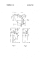
- FIG. 1 illustrates the characteristic of a transistor and different current-voltage curves when a inductive d-c circuit is switched off and on;
- FIG. 2 illustrates a transistor circuit arrangement according to the invention
- FIG. 3 illustrates a transistor circuit arrangement according to the invention in which an input transistor is connected with the main transistor, and an auxiliary voltage source is also employed.
- the characteristic of the transistor is designated by I.
- I In order to prevent a breakdown in the transistor the current and voltage transients occuring during switching must not be allowed to exceed this characteristic.
- an inductive d-c circuit If an inductive d-c circuit is switched on, one obtains the current-voltage curve in FIG. 1 designated with II, which is safely below the characteristic of the transistor.
- the shape of the current-voltage curve designated III occurs upon switching off an inductive d-c circuit if no circuit elements are provided for limiting the voltage. As will be seen from FIG. 1, the currentvoltage curve III exceeds the characteristic of the transistor, and a second breakdown of the transistor therefore occurs.
- the current voltage curve designated IV is obtained. In this curve the characteristic of the transistor is not exceeded, and a second breakdown cannot occur.
- an inductor m is connected by one terminal directly to the positive terminal +U, and its other terminal is connected to the negative terminal of a d-c voltage source through the collector-emitter path of a transistor p.
- a series circuit is connected consisting of a first and second resistor, r1 and r2.
- a diode n is arranged between the two resistors.
- the base of the transistor p is connected to the cathode of diode n and the first resistor rl is connected to the anode of diode n.
- the common junction of the resistor r1 and the anode of diode n forms the control input.
- a control switch a is connected between the control input and the negative terminal of the dc voltage source.
- a control switch a is connected between the control input and the negative terminal of the dc voltage source.
- a control switch a is connected between the control input and the negative terminal of the dc voltage source.
- the inductor m is connected in series with a main transistor p2.
- the base of the main transistor p2 is connected with the emitter of an input transistor p1, the collector of which is connected with the positive terminal of the d-c voltage source through a collector resistor r3.
- the series circuit consisting of the first and second resistors, rl and r2, with intermediate diode n, is again connected in shunt with the inductor m and the maintransistor p2.
- An auxiliary voltage source consisting of voltage Ul is provided between the second resistor and the negative terminal of the d-c voltage source.
- the capacitor k is connected between the collector and the base of the input transistor pl, with the cathode of the diode n also connected to the base of input transistor p1.
- the common junction of the first resistor rl and the anode of the diode n again constitutes the control input.
- the control switch a is again connected between the control input and the negative terminal of the dc voltage source.
- the transistor circuit arrangement according to FIG. 3 therefore is distinguished merely by the amplifier circuit for the main transistor p2 and the additional auxiliary voltage source, the significance of which will be explained later.
- the auxiliary voltage source can also be provided, for example, in a transistor circuit arrangement according to FIG. 2 between the second resistor r2 and the negative terminal of the d-c voltage source.
- the control switch a is opened at a given point in time to connect the inductor m, transistor p is turned on by resistor r1.
- the capacitor k is then discharged at approximately constant current and causes a linear drop of the voltage across the collector-emitter path of transistor p.
- Transistor p is therefore not suddenly turned on when the control switch a is opened, but is turned on over a definite time interval. The time interval is dependent upon the time constant at which capacitor k discharges. Neglecting the control current of the transistor, this time constant is determined only by the first resistor r1 and the capacitor k.
- the function of the transistor circuit arrangement according to FIG. 3 is in principle the same as in the transistor circuit arrangement according to FIG. 2.
- the control signal for the main transistor p2 is merely amplified.
- the minimum time interval, in which the main transistor p2 or the transistor p, is switched on can be varied by the auxiliary voltage source connected between the second resistor r2 and the negative terminal of the (1-0 voltage source.
- the potential at the base of the input transistor p1 is changed by the auxiliary voltage U2, so that the time interval required for turning the input and main transistors pl and p2 on is also changed thereby.
- This design is particularly useful if the transistor circuit arrangement is used in an electronic commutation arrangement for d-c motors.
- an appropriate minimum time interval for turning on the main transistor p2 is first adjusted through the auxiliary voltage U1. If after the acceleration process the starting current has decayed to the nominal current, the time interval for turning on the transistor can be changed to a value corresponding to the nominal current, for example, by disconnecting the auxiliary voltage U1 by means of a double-throw switch b. Matching to different currents is facilitated and can be done more accurately if the auxiliary voltage Ul is adjustable. By matching the time interval for turning on the transistor according to the respective load current, the switching losses are reduced to a minimum.
- a circuit for switching an inductive d-c load on and off using a transistor switch so as to avoid secondary breakdown of the transistor due to high transient voltages generated by the load comprising:
- a transistor switch having its emitter-collector path in series with the load across a d-c source
- a diode connecting the junction of said second resistor and said switch to said base having a polarity such as to permit said capacitor to be charged through said first resistor when said switch is open and discharged through said second resistor when said switch is closed.
- a circuit for switching an inductive d-c load on and off using a transistor switch so as to avoid secondary breakdown of the transistor due to high transient voltages generated by the load comprising:
- a transistor switch having its emitter-collector path in series with the load across a dc source
- an amplifier transistor having its emitter coupled to the base of said transistor switch and its collector coupled to said source;
- a second resistor having its one end connected to 5 vand Off as in Claim 3 in Which an auxiliary adjustable the other side of said source and its other end cond b h d nected through a switch to said one side of said Voltage slmrce 1S arrange etweent resistor an the one side of the d-c voltage source to permit the adsource, the value of said second resistor being sub- Stantiany greater thatn that of Said first resistor; ustment of the voltage applied to the transistor with f.
- Varying Starling clfrrems transistor is turned sistor and said switch to said base having a polarity 0 an he n uctl e -C ClrCult 8 turned on. such as to permit said capacitor to be charged
Landscapes
- Electronic Switches (AREA)
- Dc-Dc Converters (AREA)
- Relay Circuits (AREA)
Applications Claiming Priority (1)
| Application Number | Priority Date | Filing Date | Title |
|---|---|---|---|
| DE2135858A DE2135858C3 (de) | 1971-07-17 | 1971-07-17 | Transistorschalteinrichtung zum Schalten eines induktiven Gleichstromkreises |
Publications (1)
| Publication Number | Publication Date |
|---|---|
| US3829708A true US3829708A (en) | 1974-08-13 |
Family
ID=5814025
Family Applications (1)
| Application Number | Title | Priority Date | Filing Date |
|---|---|---|---|
| US00270924A Expired - Lifetime US3829708A (en) | 1971-07-17 | 1972-07-12 | Transistor switching circuit arrangement for an inductive d-c circuit |
Country Status (5)
| Country | Link |
|---|---|
| US (1) | US3829708A (enExample) |
| JP (1) | JPS5326302B1 (enExample) |
| DE (1) | DE2135858C3 (enExample) |
| FR (1) | FR2146751A5 (enExample) |
| GB (1) | GB1393306A (enExample) |
Cited By (5)
| Publication number | Priority date | Publication date | Assignee | Title |
|---|---|---|---|---|
| US4013904A (en) * | 1975-08-28 | 1977-03-22 | Westinghouse Electric Corporation | Darlington transistor switching circuit for reactive load |
| EP0220791A1 (en) * | 1985-06-18 | 1987-05-06 | Fuji Electric Co., Ltd. | Switching device |
| US5424666A (en) * | 1993-04-26 | 1995-06-13 | Consorzio Per La Ricera Sulla Microelectronica Nel Mezzogiorno | Control circuit for slowly turning off a power transistor |
| DE102016114002A1 (de) * | 2016-07-29 | 2018-02-01 | Eberspächer Controls Landau Gmbh & Co. Kg | Trennschalteranordnung, insbesondere für ein Bordspannungssystem eines Fahrzeugs |
| CN114062917A (zh) * | 2021-11-16 | 2022-02-18 | 广东电网有限责任公司 | 一种旁路开关高频耐压试验电路、方法及装置 |
Families Citing this family (2)
| Publication number | Priority date | Publication date | Assignee | Title |
|---|---|---|---|---|
| GB2242587B (en) * | 1990-02-01 | 1994-05-25 | Mole Valley Systems Ltd | Power control circuit for reactive loads |
| DE102019134525A1 (de) * | 2019-12-16 | 2021-06-17 | Valeo Siemens Eautomotive Germany Gmbh | Schaltungsanordnung und Verfahren zum Schutz eines Leistungshalbleiterschalters vor Überspannungen |
-
1971
- 1971-07-17 DE DE2135858A patent/DE2135858C3/de not_active Expired
-
1972
- 1972-07-11 FR FR7225153A patent/FR2146751A5/fr not_active Expired
- 1972-07-12 US US00270924A patent/US3829708A/en not_active Expired - Lifetime
- 1972-07-13 GB GB3289972A patent/GB1393306A/en not_active Expired
- 1972-07-17 JP JP7155072A patent/JPS5326302B1/ja active Pending
Cited By (7)
| Publication number | Priority date | Publication date | Assignee | Title |
|---|---|---|---|---|
| US4013904A (en) * | 1975-08-28 | 1977-03-22 | Westinghouse Electric Corporation | Darlington transistor switching circuit for reactive load |
| EP0220791A1 (en) * | 1985-06-18 | 1987-05-06 | Fuji Electric Co., Ltd. | Switching device |
| US5424666A (en) * | 1993-04-26 | 1995-06-13 | Consorzio Per La Ricera Sulla Microelectronica Nel Mezzogiorno | Control circuit for slowly turning off a power transistor |
| DE102016114002A1 (de) * | 2016-07-29 | 2018-02-01 | Eberspächer Controls Landau Gmbh & Co. Kg | Trennschalteranordnung, insbesondere für ein Bordspannungssystem eines Fahrzeugs |
| US10439607B2 (en) | 2016-07-29 | 2019-10-08 | Eberspächer Controls Landau Gmbh & Co. Kg | Circuit breaker device, especially for a vehicle electrical system |
| CN114062917A (zh) * | 2021-11-16 | 2022-02-18 | 广东电网有限责任公司 | 一种旁路开关高频耐压试验电路、方法及装置 |
| CN114062917B (zh) * | 2021-11-16 | 2023-08-18 | 广东电网有限责任公司 | 一种旁路开关高频耐压试验电路、方法及装置 |
Also Published As
| Publication number | Publication date |
|---|---|
| DE2135858C3 (de) | 1980-02-28 |
| DE2135858B2 (de) | 1975-01-23 |
| GB1393306A (en) | 1975-05-07 |
| DE2135858A1 (de) | 1973-02-01 |
| FR2146751A5 (enExample) | 1973-03-02 |
| JPS5326302B1 (enExample) | 1978-08-01 |
Similar Documents
| Publication | Publication Date | Title |
|---|---|---|
| US4622482A (en) | Slew rate limited driver circuit which minimizes crossover distortion | |
| US5036269A (en) | Voltage stabilizer with a very low voltage drop designed to withstand high voltage transients | |
| EP0166581A2 (en) | Cmos circuit overvoltage protection | |
| US3241043A (en) | Thyratron tube replacement unit employing a zener diode limiting the inverse voltageacross a gating transistor | |
| US5568345A (en) | Overvoltage protection circuit | |
| US3829708A (en) | Transistor switching circuit arrangement for an inductive d-c circuit | |
| US3729655A (en) | Protective circuit arrangement for a switching transistor in an inductive load circuit | |
| US3886410A (en) | Short circuit protection apparatus for a regulated power supply | |
| US4723191A (en) | Electronic voltage regulator for use in vehicles with protection against transient overvoltages | |
| WO1984002622A1 (en) | Comparator circuit having reduced input bias current | |
| US4158178A (en) | Anti-latch circuit for amplifier stage including bipolar and field-effect transistors | |
| US4420786A (en) | Polarity guard circuit | |
| US3206695A (en) | Overvoltage protection circuit for power converters | |
| EP0132863B1 (en) | Protection circuit | |
| GB871787A (en) | Transistor monostable two-state apparatus | |
| JPH027714A (ja) | 異常電流時の素子の保護装置 | |
| US4339669A (en) | Current ramping controller circuit | |
| US3106674A (en) | Regulator protection circuits | |
| US4068278A (en) | Overload protection circuit for amplifiers | |
| US3875539A (en) | High voltage ripple reduction circuit | |
| US5606481A (en) | Overvoltage protection for battery powered equipment | |
| US3508162A (en) | Means for limiting current in a power supply amplifier | |
| US4047054A (en) | Thyristor switching circuit | |
| US11177650B2 (en) | Overvoltage protection circuit | |
| EP0322000B1 (en) | Integrated logic circuit incorporating hot-carrier stress reduction and instability damping |