US3772676A - Character display system - Google Patents
Character display system Download PDFInfo
- Publication number
- US3772676A US3772676A US00245082A US3772676DA US3772676A US 3772676 A US3772676 A US 3772676A US 00245082 A US00245082 A US 00245082A US 3772676D A US3772676D A US 3772676DA US 3772676 A US3772676 A US 3772676A
- Authority
- US
- United States
- Prior art keywords
- words
- word
- character
- stroke
- stored
- Prior art date
- Legal status (The legal status is an assumption and is not a legal conclusion. Google has not performed a legal analysis and makes no representation as to the accuracy of the status listed.)
- Expired - Lifetime
Links
Images


Classifications
-
- G—PHYSICS
- G09—EDUCATION; CRYPTOGRAPHY; DISPLAY; ADVERTISING; SEALS
- G09G—ARRANGEMENTS OR CIRCUITS FOR CONTROL OF INDICATING DEVICES USING STATIC MEANS TO PRESENT VARIABLE INFORMATION
- G09G1/00—Control arrangements or circuits, of interest only in connection with cathode-ray tube indicators; General aspects or details, e.g. selection emphasis on particular characters, dashed line or dotted line generation; Preprocessing of data
- G09G1/06—Control arrangements or circuits, of interest only in connection with cathode-ray tube indicators; General aspects or details, e.g. selection emphasis on particular characters, dashed line or dotted line generation; Preprocessing of data using single beam tubes, e.g. three-dimensional or perspective representation, rotation or translation of display pattern, hidden lines, shadows
- G09G1/08—Control arrangements or circuits, of interest only in connection with cathode-ray tube indicators; General aspects or details, e.g. selection emphasis on particular characters, dashed line or dotted line generation; Preprocessing of data using single beam tubes, e.g. three-dimensional or perspective representation, rotation or translation of display pattern, hidden lines, shadows the beam directly tracing characters, the information to be displayed controlling the deflection and the intensity as a function of time in two spatial co-ordinates, e.g. according to a cartesian co-ordinate system
- G09G1/10—Control arrangements or circuits, of interest only in connection with cathode-ray tube indicators; General aspects or details, e.g. selection emphasis on particular characters, dashed line or dotted line generation; Preprocessing of data using single beam tubes, e.g. three-dimensional or perspective representation, rotation or translation of display pattern, hidden lines, shadows the beam directly tracing characters, the information to be displayed controlling the deflection and the intensity as a function of time in two spatial co-ordinates, e.g. according to a cartesian co-ordinate system the deflection signals being produced by essentially digital means, e.g. incrementally
Definitions
- the [58] 6 ig word for each stroke contains an auxiliary bit 1 340/324 which specifies if the follow-stroke is to be a continua- 8 tion of the presently read stroke so that a separate word for the following stroke need not be stored.
- the [56] References and Read Only Memory is divided into blocks wherein UNITED STATES PATENTS each block contains the stroke groups for two charac- 3,533,096 10/1970 Bouchard 340/324 A ters-one group at each end of the block, and the 3,540,032 11/1970 Criscimagna et a1. 340/324 A groups are paired according to size to minimize storage space. Primary Examiner-David L.
- This invention relates generally to character display systems which are capable of displaying any combination of a repertoire of characters on a surface such as an X-Y table or the viewing screen of a cathode ray tube.
- the invention relates more particularly to systems in which the characters are formed by successive strokes of a marker such as a pen or an electron beam, as opposed to systems using a raster technique as in home television.
- a computer has stored in its memory any instruction set indicative of the messages to be displayed. These instructions are passed to a character display system, one character at a time.
- a character display system of the stroke tracing type In response to the instruction to display a particular character, a character display system of the stroke tracing type must generate a succession of X and Y deflection signals which direct the movement of the marker as it traces each stroke of the character. It must also generate another signal, sometimes called an intensity signal, which directs the marker either to write as it moves or to not write as it moves to a new position. All of these signals are applied through suitable buffers, amplifiers and the like, to the actual display device which traces out the characters.
- Anotherobject is to provide a character display system of reduced size. 7
- Another object is to provide a character display system in which the memory portion is readily manufactured.
- Another object is to provide a character display system with improvedcharacter definition.
- a display system incorporating the present invention stores the stroke patterns for the individual characters in digital form in a Read Only Memory.
- Each stroke for each character is defined as a word.
- Each character is permitted a maximum of a first predetermined number of strokes.
- a second predetermined number of word spaces is allotted for storing the strokes for two characters.
- the second predetermined number may be substantially less than twice the first predetermined number.
- the two characters to be stored in each allotted space are paired in advance.
- the words representing strokes for one of the characters are stored beginning at one end of the allotted space, while the words representing the strokes of the other character are stored beginning at the opposite end of the allotted space.
- Certain redundancies are eliminated. If two successive words are identical, the storage of the second is omitted.
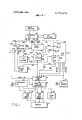
- FIG. 1 is a functional block diagram of a display system incorporating the present invention
- FIG. 2 is a diagram showing the relative times of occurrence of various waveforms
- FIG. 3 is a schematic block diagram of the timing control and Gate Generator circuits
- FIG. 4 is a Memory Map, or Pattern Location diagram, showing schematically the arrangement of the various units of the Read Only Memory
- FIG. 5 is a schematic diagram showing the connections among the various units of the Memory
- FIG. 6 is a diagram showing the arrangement of word storage in a portion of the Memory
- FIG. 7 is a diagram of the strokes used to write the character
- FIG. 8 is a diagram of the strokes used to write the character A;
- FIG. 9 is a diagram illustrating the various strokes which may be traced in the first quadrant.
- FIG. 10 is a schematic block diagram of the clock modifying circuit and other portions of the apparatus.
- FIG. 11 is a diagram showing the relative times of occurrence of additional waveforms.
- FIG. 12 is a schematic block diagram of the End of Character Decoder.
- the character data path 25 transmits, one at a time, digital words each representing a character or symbol to be displayed and the path 25 comprises as many conductors as are required to transmit all the bits of each such word simultaneously.
- a bus or path is applied as an input or output to a gate or a component, it is to be understood that the number of gates or the number of terminals of the component are sufficient to accommodate all of the conductors of that bus or path.
- the computer 21 has a memory in which are stored in digital form words representing characters to be displayed on the display device 26 which is considered, for illustrative purposes, to be a cathode ray tube (CRT) device.
- the memory of computer 21 also has stored therein instructions as to the sequence, timing and position at which characters are to be displayed on the device 26.
- words representing the character and its position are applied to the paths 25 and 27 respectively for transmission to the system 24.
- a start signal is then sent over the path 28 to the system 24 which immediately generates a busy signal and transmits it to the interface unit 22 over the path 29 so as to suspend receipt of further instructions until the instant character is displayed.
- the system 24 then writes" the specified character on the device 26, in a manner to be more fully explained, and, when finished, removes the busy signal, thereby enabling reception of further instructions.
- Each set of instructions in the memory of the computer 21 may be updated by means of a stored program contained therein and/or by means of various peripheral devices 23 such as photopens, tape or card reading devices, keyboard devices, and the like.
- the updating or current sensor data is coupled via the interface unit 22 to the computer 21 where it is processed according to the stored program to update the instructions.
- the character display system 24 includes timing control and gate generating circuits 30 which control the operation of the system by means of various clocks, pulses, gates and other waveforms as illustrated in FIG. 2.
- timing control and gate generating circuits 30 which control the operation of the system by means of various clocks, pulses, gates and other waveforms as illustrated in FIG. 2.
- a logical l is represented by a positive voltage (approximately 4 volts) also referred to as I-Iigh" or hi
- a logical is represented by approximately zero volts, also referred to as low” or the flip flop circuits (FF) require an inverted or low signal to reset them directly, as indicated by the conventional inverter symbol on each of these inputs
- the basic clock is a positive going square wave with a period of 75 nanoseconds (ns) although a 150 ns clock derived therefrom is also used
- the flip flops and other circuits operated by clock pulses are actuated on the descending, or negative going portion of the pulse.
- FIG. 3 there is shown the previously mentioned clock 31, designated Clock A, the output of which is connected to a conductor 32 for distribution to various components. Connection to such components is shown in FIG. 3 by a short arrow labeled A".
- the waveform of this clock is shown by the curve 41 of FIG. 2.
- the start pulse has the waveform shown by the curve 42 of FIG. 2 and is a negative going pulse whose duration is not critical but is preferably in the range from about ns to 300 ns.
- the conductor 28 carrying this pulse is connected through an inverting amplifier 33 to one of the J inputs of a flip flop circuit 34, which is operated by the clock 31.
- the Q output of the flip flop 34 is connected to its K input.
- the Q output is connected through an inverter to the SET input of a flip flop 35.
- the Q output of the latter flip flop is connected to the conductor 29 to carry the busy signal back to the interface unit 22.
- the 6 output of the flip flop 35 is connected to the J input of the flip flop 34.
- both the J and K inputs of the flip flop 34 are low and accordingly the clock has no effect.
- the J input goes high whereupon the next occurring negatively going portion of the clock pulse makes the Q output high and the Q output low.
- SETS the flip flop 35 so that the Q output goes high and constitutes the busy signal.
- the above mentioned negative going portion of the pulse of clock A is designated time 0.
- the busy signal is a high level signal starting at time 0 but of indefinite duration, being terminated only when the writing of the character is completed, all as will be more fully explained.
- the next clock pulse at time 75 returns the flip flop 34 to its initial conditions. Because both the J and K inputs are now low, further action of this flip flop must await both the removal of the character busy signal and the arrival of another start pulse.
- the Q output of the flip flop 34 is also connected to the J input of another flip flop 36, also actuated by Clock A, the Q output of which is connected back to its own K input.
- the Q output of the flip flop 34 goes high at time 0, in the sequence previously explained, it makes the J input of the flip flop 36 high so that the next succeeding clock pulse, at time 75, actuates this flip flop to make the Q output high and the 6 output low.
- the 6 output remains low until the arrival of the next clock pulse at time whereupon the flip flop 36 is returned to its initial condition.
- This Q output, carrying the waveform 44 is connected to a conductor 37 and constitutes a gate which enables certain other portions of the apparatus, as will be more fully explained.
- the path 25 carrying the character data is connected to a latch circuit 51.
- This data is preferably in the form of a 7 bit digital word representing the desired character in accordance with a predetermined code such as the U.S.A. Standard Code for Information Interchange (ASCII).
- ASCII Standard Code for Information Interchange
- the bits of the word are transmitted simultaneously over a multiplicity of conductors.
- a latch circuit such as the latch 51, is a form of temporary digital storage.
- the bits to be stored are applied in parallel as voltage levels to the input.
- the output terminals assume the voltage levels dictated by the input. These outputs continue to be available after termination of the enabling pulse and remain unchanged regardless of the input. Upon receipt of another enabling pulse, the outputs assume the voltage levels dictated by the then present input.
- Such latches are well known and are available commercially from several manufacturers.
- One kind suitable for use in the present invention is that marketed by the Fairchild Semiconductor Division of Fairchild Camera and Instrument Corp., Mountainview, Calif, and designated Model 9314.
- the latch 51 may comprise two such units.
- the waveform 44 illustrated in FIG. 2 is applied over the conductor 37 to the latch circuit 51 whereupon voltage levels indicative of the various bits of the word appear on the output. Different bits of the word are transmitted to different portions of the apparatus, as will be more fully explained.
- a Read Only Memory (ROM) 52 is also shown in FIG. 1 .
- ROM Read Only Memory
- Such a memory is a digital storage device containing information which cannot be altered during normal operation of the device. The desired storage pattern is inserted during manufacture, that is, before use. All of the bits of each stored digital word are stored at a single address, which, upon the application of a suitable voltage level, cause voltage levels indicative of each bit in the addressed word to appear in parallel, simultaneously, at the output terminals (which are equal in number to the number of bits in each word) for as long as the applied voltage persists.
- Such Read Only Memory devices are well known and are available commercially from several manufacturers, on example suitable for present purposes being that marketed by the Intel Corp., Mountainview, Calif. as model no. 3301.
- This functional arrangement of the 16 units which constitute the Read Only Memory 52 The units are arranged in pairs so that each pair stores 256 8 bit words.
- the physical arrangement may, of course, be anything which is convenient for mounting and wiring but, for explanation, it is convenient to think of the units as being arranged in the rows and columns of the ASCII code.
- the units 52a, 52b etc. are shown one below the other across the top of the Figure.
- the words are assumed to extend horizontally, side by side, with the bits of each word being arranged in vertical rows.
- Each unit is assumed to be divided into 8 blocks of 32 words each containing 4 bits.
- each pair of units such as the pair 52a and 52b, is arranged into 8 blocks of addresses, each block containing 32 addresses and each address containing 1 word of 8 bits.
- the remaining units of the memory 52 are designated 52c to 52p inclusive and are arranged beneath the pair 520 and 52b as shown. These pairs are also assumed to be divided into 8 blocks of 32 addresses each. Each block of each pair of units stores the words representing the strokes required to write 2 characters. In the embodiment being described, there are a total of 64 blocks each storing the words necessary to write 2 characters so that a total of 128 characters is provided for.
- the present invention stores the words defining the strokes for two characters in a total of 32 addresses. This is possible for a number of reasons. First, not all characters will require a full 25 strokes so that it is possible to pair a character requiring many strokes with a character requiring few strokes. Additionally, not every stroke requires a separate address, that is, a separate word definition. For example, if the second stroke of a character is to be the same as the first stroke, the word defining the first stroke may include a bit indicating that the next stroke is identical. This being so, his unnecessary to provide a separate address for the second stroke. This will be explained more fully.
- Each of the units for example, the unit 52a, includes 8 address inputs designated A0 to A7 inclusive.
- Each unit is manufactured with an internal decoder so that when it is addressed by an 8 bit code applied to the terminals A0 to A7, one of the 32 addresses has a voltage level applied thereto and thereby is activated.
- the digital output indicative of the words stored at the particular address appears on the four output terminals, 01 to 04, inclusive.
- Each unit also includes a terminal designated Vcc to which the supply voltage is connected and a terminal designated GND which is connected to ground.
- Each unit also has two terminals designated CS1 and CS2 (which are abbreviations for Chip Select 1 and Chip Select 2). These terminals are connected to enable a matrix of internal OR gates connected in the output leads. No output signal will appear on any of the output terminals 01 to 04 inclusive unless a suitable enabling signal is applied to both of the terminals CS1 and CS2.
- the address terminals A0 to A7 inclusive of all of the units are connected in parallel.
- the CS1 terminals of the two units constituting each pair are connected together. That is, the CS1 terminals of units 52a and 52b, which constitute column 0 are connected together. Similarly, the CS1 terminals of units 52c and 52d which constitute column 1, are connected together, and the remaining units are similarly connected. All of the CS2 terminals are connected together so that the entire memory 52 can be enabled or disabled with a single signal.
- the output terminals 01 to 04 of all of the first units of each pair are connected together as are the output terminals of all of the second units of each pair. That is, the output terminals of units 52a, 52c, 52e, etc., are connected together and the output terminals of units 52b, 52d, and 52f etc., are all connected together.
- the Q output of the flip flop 36 is connected to the J input of a flip flop 55 the Q output of which is connected to the J input of another flip flop 56.
- the flip flops are both actuated by the clock A.
- the Q output of the flip flop 56 is connected to the K inputs of both of the flip flop 55 and 56, while the Q output of the flip flop 55 is connected by a conductor 57 to the J input of a flip flop 58.
- the Q output of the latter is connected to its K input and to the J input of a flip flop 59, the Q output of which is connected to its own K input.
- the flip flops 58 and 59 are also actuated by the Clock A.
- the Q output of the flip flop 58 is connected to a conductor 60 so as to control other portions of the apparatus, as will be more fully explained.
- Q55 and conductor 57 go low. Also at time 300, Q59 goes high while Q 59 goes low.
- the voltage of Q59, and the voltage of conductor 29, carrying the character busy signal are used to generate a reset integrator" signal which directs the establishment and renewal of a suitable resetting circuit such as one which discharges the capacitors used in the function generator or otherwise prepares the function generator for a new operation.
- a pair of NAND circuits 61 and 62 each comprising an AND circuit with an inverter in the output are connected as a flip flop. More particularly, the conductor 29 is connected to one input of the circuit 61, while the Q output of flip flop 59 is connected to one input of the other circuit 62.
- the output of circuit 61 is connected to the other input of circuit 62 and the output of circuit 62 is connected to the other input of circuit 61.
- the output conductor 63 is connected to the output of circuit 61. Initially, that is, after the completion of one character and before starting the next, the conductor 29 (see waveform 43 FIG. 2) is low while Q 59 is high. Accordingly, the output of circuit 61 is high.
- the reset integrators signal on conductor 63 is also used to enable the generation of a 150 ns clock.
- Conductor 63 is connected through an inverting amplifier 64 to the Reset" terminal of a flip flop 66.
- This flip flop is also actuated by the clock A and has both its J and K inputs permanently connected to a high voltage source.
- the Q output is the desired 150 ns clock, designated clock B, and is connected to a conductor 67.
- the conductor 63 is high, as shown by the waveform 46 of FIG. 2, and the flip flop 66 is Reset so that the Q output is low.
- the Reset" signal is removed so that, beginning with the next clock pulse at time 375, the flip flop 66 toggles, thereby generating a 150 ns clock (clock B) on conv ductor 67 as shown by waveform 47 of FIG. 2.
- the clock C shown by the waveform 47, is derived from clock B and, as far as those portions shown in FIG. 2 are concerned, is substantially identical to clock B. It differs when a SKIP is called for as will be more fully explained subsequently.
- the output of the latch circuit 51 is a 7 bit ASCII word which defines the next character to be written.
- the three most significant bits of this word are connected over a path 71 to the A5, A6, and A7 address terminals of the memory 52. These three bits select one of the address blocks of the memory 52. Referring to FIG. 4, these bits select that block of all the units which represents one of the double rows such as the rows 0 and 1 or the rows 2 and 3 or the rows 4 and 5, etc.
- the decoder 73 is a conventional device which places a signal on that one of eight output conductors which is designated by the input signal. These output conductors are represented collectively by the path 74 and are connected to the CS1 terminals of those units representing columns 0 to column 7 respectively. In other words, the first conductor is connected to the CS1 terminals of units 52a and 52b, the next conductor is connected to the CS1 terminals of units 520 and 52d, etc. Referring again to FIG. 4 the decoder 73 selects the column. Thus, the first six bits together have selected one block of addresses in one particular pair of units. Each one of these blocks of addresses, as previously mentioned, contains the words representing the strokes for two characters and it is necessary to select between them.
- the last bit of the ASCII code from the latch circuit 51 is connected over a path 75 to an up/down counter 76.
- This counter is a conventional five bit unit, and, in response to successive clock pulses, generates successive five bit signals on five output conductors running successively up from 00000 to 11 1 l l or alternatively, running down from I l I l l to 00000. Whether it counts up or down is selected by the last bit applied thereto over the path 75.
- the five conductors of the output are represented by the path 77 and are applied to the address inputs A0 to A4 inclusive of the memory 52.
- the counter 76 is controlled by a nanosecond clock C, indicated by the waveform 47 of FIG. 2, which is a modified version of the clock B. Modification is accomplished by a clock modifying circuit 78 the function and operation of which will be explained subsequently.
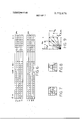
- FIG. 6 there are shown the portions of the units 52g and 52h corresponding to ASCII column 4 and ASCII rows 0, 1.
- this address block are stored two groups of words, one representing the pattern of required strokes to write the character (h and the other representing the pattern of strokes required to write the Capital A.
- the first group representing has nineteen words which are stored in adjacent addresses starting at the left end of the block.
- the second group, representing A has nine words which are stored in adjacent addresses starting at the right end of the block.
- There'are 32 addresses in the block each capable of storing an 8 bit word, although not all the addresses are used.
- the various ones and zeros represent the digits stored in each space.
- FIG. 7 there are shown schematically 22 strokes used to write the character
- the instructions for these strokes are shown in coded form in the left hand portion of FIG. 6.
- FIG. 8 shows the 12 strokes required to write the capital A.
- the instructions for these strokes are shown in coded form on the right hand portion of FIG. 6.
- each instruction is an 8 bit word and the bits are designated, from top to bottom in FIG. 6, as X X X Y Y Y U8 and SK.
- These codes have the meanings shown in Table I. 25 quently.
- Y outputs are passed to a decoder and buffer matrix 81 which is controlled by the same clock C as controls the up/down counter 76.
- the outputs are decoded into terms of the desired X and Y motions of the beam, stored temporarily, and passed to a function generator 82 which may include integrators and be generally similar to that described in the aforementioned US. Pat. No. 3,533,096.
- the outputs of the function generator 82 are combined with the outputs of a positioning circuit 83 in an X sum and drive amplifier 84 and a Y sum and drive amplifier 85 and are then passed to the display 26.
- the X6, Xi, and X7 outputs are also passed to an EC decoder 86 which decodes them to generate an EC (end of character) signal after the character has been written.
- This signal is transmitted via the path 87 to the K input of the flip flop (FIG. 3) so that the character busy signal is removed at the next clock pulse.
- the reset integrator waveform is applied via the path 63 to the decoder 81 and to the function generator 82 so as to make them ready for the next character.
- the SK output of the memory 52 is transmitted over a path 88 to the clock modification circuit 78 the details of which will be explained subse- The F?
- the outputs of the memory 52 are coded digital signals indicative of the rate and direction of movement and intensity required of a marker to write the selected character. It is possible to trace lines in various directions for various distances in each unit of time. Regarding the X direction first, it is possible to trace lines in either the positive or the negative direction a distance equal to one half of one of the spaces indicated in FIGS. 7 and 8, or a whole space, or one and one half spaces. Similarly, lines can traced in the Y direction, either positively or negatively by corresponding amounts.
- the starting position of the marker is the point S at the lower left hand corner as shown in FIGS. 7 and 8.
- the U8 (unblank) signal is used to control the intensity of the beam, that is, whether to leave it blanked out so that the beam does not write anything or to unblank it causing it to write.
- the SK (skip) signal is used to indicate whether the next succeeding stroke is the same as the one now being written, as will be more fully explained.
- the particular units used to form the memory 52 provide for low or zero outputs as logical ones. Accordingly, in terms of the logic used throughout the rest of the equipment, the outputs are Y0, X1, X1, Y8, YT, Y7, UH and SK All six of the X able buffering, is transmitted to a Z drive amplifier 89 which, in turn, controls the intensity of the display device 26.
- the first bit X is a one which indicates that the motion of the marker, which, in this case, is the beam of the CRT, in the X direction is positive.
- the next 2 bits, X and X are 0 and 1 respectively, indicating, as shown by Table I, that the beam is to move one half a space as those spaces are indicated in FIGS. 7 and 8.
- the Y output is a 1 indicating that the beam is to move positively in the Y direction.
- the Y1 and Y2 outputs are l and 0, respectively, indicating that the beam is to move one Y space during this period.
- the U8 bit is a 1 indicating that the beam should be unblanked so that a visible trace will be made.
- the skip pulse is also a 1 indicating that the second stroke is identical to the first. Therefore, it is unnecessary to store this second word since it is merely a duplication of the first.
- the writing of the second stroke is accomplished by skipping a clock pulse so that the decoder and buffer matrix 81 maintains its outputs unchanged for another clock period with the result that the function generator 82 continues to generate ramp voltages at the same rates as before.
- the apparatus by which the outputs are maintained by skipping a pulse is shown in detail in FIG. 10.
- the skip function will be explained with the aid of a simplified example.
- the Read Only Memory 52 including the internal decoder 52r which receives the 5 bit count over the path 77 from the up/- down counter 76.
- the decoder 52r activates, that is, reads out, the words in the selected group of addresses successively. For illustrative purposes only four addresses are shown.
- the skip output of the memory 52 is transmitted over the path 88 to the clock modifying circuit 78. More particularly, the path 88 is connected to the input of an inverting amplifier 78a the output of which is connected to the J input of a flip flop 78b which flip flop is actuated by the clock B. The Q output of the flip flop 78b is connected to its own K input. The reset terminal is connected to the conductor 60 which, it will be recalled from the discussion of FIGS. 1, 2 and 3, carries a negative going skip reset" pulse of seventy five nanoseconds duration beginning at time 225. The 6 output which is now a one is connected to one input of an AND circuit 780 the other input of which is connected to the conductor 67 carrying the clock B. The output of the AND circuit is connected by means of a path 90 to the up/down counter 76 and to the decoder and buffer matrix 81.
- FIG. 11 shows the state of the U/D counter 76 and the various waveforms associated with the illustrative example of FIG. 10.
- the counter 76 Prior to time 300 (300 ms after generation of the character busy signal) the counter 76 had been reset to 00000, as previously explained, and therefore the first word of the example had already appeared at the output of the ROM 52. Since X, is zero, the X, output is high at this time as indicated by the waveform 93. Similarly, Y, is one and the X, output is low as indicated by the waveform 95. Skip is zero and the ST output is high as shown by the waveform 97.
- the J input to the flip flop 78b is low, as shown by the waveform 98, and the 6 output remains high (having been reset) as shown by the waveform 99.
- Both this X and Y outputs of the buffer 81 are high, as indicated by the waveforms 94 and 96 respectively, due to the previous action of the reset integrator signal (waveform 46 of FIGS. 2 and 11).
- the reset integrator signal is removed from the decoder and buffer 81 and from the function generator 82 thereby conditioning these components to utilize new inputs. Seventy five nanoseconds later the first positive going portion of Clock B (Waveform 47) is generated. Since 6 of flip flop 78b is high, this portion of clock B on conductor 67 (FIG. 10) passes through the AND circuit 780 and appears on conductor as clock C (waveform 48).
- the clock C is also applied to the U/D counter 76 and the negative going portion at time 450 initiates the changing of the count from 00000 to 00001 and the reading of the second word from the ROM 52.
- X,, Y,, and SK of the second word are one, zero and one respectively, and accordingly the X T, and SX outputs of the ROM 52 go low, high and low, respectively N nanoseconds after time 450, as shown by the waveforms 93, and 97. This low skip output, after inversion makes the J input of the flip flop 78b high immediately, as shown by the waveform 98.
- the negative going portion of the clock C actuates the flip flops 81a and 81b so that the X and X outputs of the buffer 81 go low and high respectively to indicate the corresponding values in the second word.
- clock C is also applied to the U/D counter 76 thereby initiating the changing of the count from 00001 to 00010 and the reading of the third word from the ROM 52.
- the negative going portion of clock B is applied to the flip flop 78b and, since J is high, 6 becomes low as shown by the waveform 99 of FIG. 1 1.
- This low condition blocks the AND circuit 78c so that the next positive going portion of clock B (occurring at time 675) cannot pass through, thereby inhibiting what would normally be the corresponding pulse of clock C.
- the pulse thus inhibited is shown by the dotted portion of the waveform 48 in FIG. 11. since there is no negative going portion of clock C at time 750, none is applied to the decoder and buffer 81 at this time.
- the X output remains low and the Y output remains high as shown by the waveforms 94 and 96, and the function generator 82 continues to generate ramp voltages at the same rates as before.
- clock C actuates the buffer 81 to reflect the outputs corresponding to the third word, that is, X high and Y low. Also, the counter 76 is advanced to 00011 and N nanoseconds later the outputs of the ROM 52 correspond to the fourth word, namely, 3C, low and Y; also low.
- each word appears at the output of the buffer during the clock period next following that in which it first appears at the output of the memory.
- the effect of the skip signal in any word is to hold or store that word in the buffer for an additional clock period and to simultaneously hold or store the next succeeding word at the memory output for the same additional clock period.
- the next word is read out beginning at the start of the fifth writing time period. This word is all zeros. This directs the beam to remain stationary at its then attained position but blanked out for one time period.
- the reason for this is that the variousamplifiers have finite band widths and it is found, if it is attempted to radically alter the direction of an unblanked beam such as that occurring at the apex of the A, that the beam never quite reaches the apex but tends to follow an are as it reverses direction, never quite reaching the full height of the character. If such a character, for example A, is written adjacent to another character, such as a Z, with a horizontal portion at the top, the letter A will appear to be substantially shorter than the letter Z.
- the fourth word is read during the sixth writing time period and directs the beam downward from the apex of the A. It is'thought that the explanation of this and the succeeding words will be obvious from that previously given and need not be discussed in detail. It is,
- the beam is again held stationary during the tenth writing time period for the same reasons as that it was held stationary at the top of the A. It is also noted that during the 1 1th and 12th time periods the beam is blanked out because it is retracing a previously written path. Additionally, after the A has been completely written, the next and last word, read during the fifteenth time period, is coded to denote the end of the character by making X0 1, X1 0, and X2 0. When this occurs, the EC decoder 86 generates a signal which is passed to the K input of the flip flop 35 (FIG. 3) so that at the next clock pulse, Q goes low thereby removing the character busy signal.
- this removal of the busy signal on path 29 signals the interface unit 22 that the system 24 is now in condition to receive instructions to write another character.
- the end of character signal initiates the generation of the reset integrator signal which prepares the decoder matrix 81 and the function generator 82 to write the next character.
- the End of Character (EC) decoder is shown in FIG. 12.
- the X output of the memory 52 is connected to the input of an inverting amplifier 101 the output of which is connected to one input of an AND circuit 102.
- the X: and Y outputs of the memory 52 are connected to first and second inputs of an AND circuit 103 the output of which is connected to the other input of an AND circuit 102. It is apparent that the output of the latter circuit will be one when and only when X 1, X, 0 and X 0.
- the end of character signal is shown by the waveform 49 of FIG. 2.
- a back up, or fail safe feature is provided in case there is no end of character word encoded in the block being addressed. Such absence could occur if, for example, in some case it were necessary to use all 32 positions in one of the blocks for words representing strokes, leaving no place for an end of character word. As another example, it is possible that one or more blocks might be unused, yet might be interrogated. In either case, operations should be terminated just as if an end of character word were present.
- the U/D counter 76 includes an ouput on conductor 105 which is normally low but which goes high after the counter has completed thirty two counts in either direction. The conductor 105 is also connected to the K input of the flip flop 35 (which has an internal OR circuit) so that, should there be no end of character signal, the end of count signal from the counter 76 will terminate operations.
- the character is written in similar manner by reading that portion of the unit 52g and 52h which is illustrated in FIG. 6, starting at the left. It is thought that the manner in which it is written will be apparent from the discussion previously given in connection with a capital A. However, it is to be noted that there are no directions for the beam to dwell for one time period, as there were for the letter A. This is because, although the illustrated stroke pattern for the character prescribes several sharp corners, none form a point at either the top or the bottom of the character. In the case of the character a slight rounding effect is beneficial rather than detrimental. It is also to be noted that the entire character is written in 22 time periods and that another one is used for the end of character code. However, only ninteen words are required to completely define the character. It is also to be noted that the character and the letter A are quite suitable to be paired because, although the character requires many strokes, the character A requires fewer strokes and both are easily fitted into the 32 word spaces with some to spare.
- an actual commercial embodiment of a system in accordance with the invention may include many additional features which have been omitted from the present disclosure in the interest of clarity. For example, it is possible to incorporate the features of writing at various speeds and/or writing characters in different sizes. Additionally, in some situations it may be desired to start the letter at the center of the space rather than at the lower left hand corner as illustrated. However, all of these techniques are well known to those skilled in the art.
- a stroke signal generating system comprising,
- a memory for storing a plurality of groups of digital words, each word representing in coded form a stroke to be traced, each group representing the strokes required to write one character,
- said memory being divided into a plurality of blocks each having the same number of adjacent addresses and each block being for storing two groups of words at addresses beginning at opposite ends thereof,
- said means for selecting and for reading includes an updown counter for sequentially reading words in the selected block beginning at that end determined by the counting direction selected.
- each of said words includes coded information specifying whether the next stroke shall be defined as a continuation of the instant stroke or whether it shall be defined by the next succeeding word.
- a stroke signal generating system including signal generating apparatus for deriving signals suitable for directing a marker to traverse any of a plurality of predetermined patterns of strokes, each pattern representing a different character, wherein said apparatus comprises,
- a memory for storing a plurality of digital words, each representing in coded form a stroke to be traced in a predetermined direction in a predetermined time, said words being stored in groups, each group representing the pattern of strokes required for one character, said memory being divided into a plurality of blocks each containing the same number of addresses and each being for storing a pair of groups of words corresponding to a preselected pair of characters, one of the groups of each pair being stored at those adjacent addresses beginning at one end of its blocks while the other group of each pair is stored at those adjacent addresses beginning at the other end of its block,
- first means responsive to an instruction to write a particular character for selecting that block in which the corresponding group of words is stored
- second means responsive to an instruction to write a particular character for selecting that end of the selected block in which the group of words corresponding to that particular character is stored and for reading sequentially the words in that group which are stored at addresses beginning at the selected end, and
- each of said groups includes a word specifying that the pattern has been completed.
- each group that includes two words calling for successive strokes having opposite vertical directions at the top or bottom of the pattern includes an auxiliary word, interposed between said two words, containing coded instructions to blank said marker and hold it at its then attained position.
- said second means includes an up-down counter, conditioned by said instruction to count either up or down depending upon the end of the selected block in which the corresponding group of words is stored, said counter being for reading sequentially the words of that group which are stored at addresses beginning at the selected end.
- a stroke signal generating system comprising circuitry, responsive to an instruction to write a selected one of a repertoire of characters, for generating a series of signals indicative of the direction of movement and writing intensity required of a marker to trace the selected character, characterized in that such circuitry includes a memory having stored therein a plurality of digital words arranged in groups, each word representing in coded form the characteristics of a stroke, each group representing the characteristics of all the strokes required to write one character, characterized in that said memory is divided into a plurality of blocks of addresses, each block being for storing two groups of words at addresses beginning at opposite ends thereof, and in that said circuitry includes means responsive to the aforesaid instruction for selecting that block in which the group of words corresponding to the selected character is stored and for reading the words of one of the groups stored in that block beginning at one or the other end of the block depending upon which end includes addresses of words in the group corresponding to the selected character, whereby the required series of signals is generated.
- a system comprising,
- a memory having stored therein a plurality of digital words each defining in coded form a stroke to be traced
- each of said words including an auxiliary bit having a first or second condition specifying whether or not, respectively, the next stroke shall be defined as a continuation of the instant stroke
- a decoder and buffer actuated by pulses for decoding each word, exclusive of said auxiliary bit, after being'read out of said memory and for storing the decoded information temporarily pending receipt of a subsequent pulse
- said means responsive includes means for inhibiting that pulse next following the pulse which initiates decoding of that word which included said first condition.
- said circuit includes an AND circuit interposed between said clock and said counter and said decoder and buffer and in which said means responsive includes means for blocking the passage through said AND circuit of that pulse next following the pulse which initiated decoding of that word which included said first condition.
- said means responsive includes a flip flop circuit actuated by pulses received directly from said clock and enabled by the reading out of said first condition for blocking said AND circuit.
Landscapes
- Engineering & Computer Science (AREA)
- Radar, Positioning & Navigation (AREA)
- Remote Sensing (AREA)
- Physics & Mathematics (AREA)
- Computer Hardware Design (AREA)
- General Physics & Mathematics (AREA)
- Theoretical Computer Science (AREA)
- Controls And Circuits For Display Device (AREA)
Applications Claiming Priority (1)
| Application Number | Priority Date | Filing Date | Title |
|---|---|---|---|
| US24508272A | 1972-04-18 | 1972-04-18 |
Publications (1)
| Publication Number | Publication Date |
|---|---|
| US3772676A true US3772676A (en) | 1973-11-13 |
Family
ID=22925203
Family Applications (1)
| Application Number | Title | Priority Date | Filing Date |
|---|---|---|---|
| US00245082A Expired - Lifetime US3772676A (en) | 1972-04-18 | 1972-04-18 | Character display system |
Country Status (5)
Cited By (3)
| Publication number | Priority date | Publication date | Assignee | Title |
|---|---|---|---|---|
| US4131883A (en) * | 1976-01-20 | 1978-12-26 | Asea Aktiebolag | Character generator |
| US4156915A (en) * | 1977-03-28 | 1979-05-29 | Vector General, Inc. | Font generating system |
| US4250562A (en) * | 1979-05-22 | 1981-02-10 | Hewlett-Packard Company | Digital signal state analyzer and display |
Families Citing this family (1)
| Publication number | Priority date | Publication date | Assignee | Title |
|---|---|---|---|---|
| US4181955A (en) * | 1978-06-02 | 1980-01-01 | Mathematical Applications Group, Inc. | Apparatus for producing photographic slides |
Citations (2)
| Publication number | Priority date | Publication date | Assignee | Title |
|---|---|---|---|---|
| US3533096A (en) * | 1967-09-01 | 1970-10-06 | Sanders Associates Inc | Character display system |
| US3540032A (en) * | 1968-01-12 | 1970-11-10 | Ibm | Display system using cathode ray tube deflection yoke non-linearity to obtain curved strokes |
Family Cites Families (2)
| Publication number | Priority date | Publication date | Assignee | Title |
|---|---|---|---|---|
| FR2029264A5 (US06252093-20010626-C00008.png) * | 1969-01-22 | 1970-10-16 | Vincent Carrefour Jacque | |
| US3717872A (en) * | 1970-06-01 | 1973-02-20 | Hughes Aircraft Co | High fidelity symbol display through limited bandwidth system |
-
1972
- 1972-04-18 US US00245082A patent/US3772676A/en not_active Expired - Lifetime
-
1973
- 1973-02-09 CA CA163,404A patent/CA999682A/en not_active Expired
- 1973-03-15 DE DE2313016A patent/DE2313016C2/de not_active Expired
- 1973-04-17 GB GB1855973A patent/GB1423716A/en not_active Expired
- 1973-04-18 JP JP4401573A patent/JPS5721716B2/ja not_active Expired
Patent Citations (2)
| Publication number | Priority date | Publication date | Assignee | Title |
|---|---|---|---|---|
| US3533096A (en) * | 1967-09-01 | 1970-10-06 | Sanders Associates Inc | Character display system |
| US3540032A (en) * | 1968-01-12 | 1970-11-10 | Ibm | Display system using cathode ray tube deflection yoke non-linearity to obtain curved strokes |
Cited By (3)
| Publication number | Priority date | Publication date | Assignee | Title |
|---|---|---|---|---|
| US4131883A (en) * | 1976-01-20 | 1978-12-26 | Asea Aktiebolag | Character generator |
| US4156915A (en) * | 1977-03-28 | 1979-05-29 | Vector General, Inc. | Font generating system |
| US4250562A (en) * | 1979-05-22 | 1981-02-10 | Hewlett-Packard Company | Digital signal state analyzer and display |
Also Published As
| Publication number | Publication date |
|---|---|
| JPS4948249A (US06252093-20010626-C00008.png) | 1974-05-10 |
| JPS5721716B2 (US06252093-20010626-C00008.png) | 1982-05-08 |
| DE2313016A1 (de) | 1973-11-08 |
| GB1423716A (en) | 1976-02-04 |
| DE2313016C2 (de) | 1985-01-10 |
| CA999682A (en) | 1976-11-09 |
Similar Documents
| Publication | Publication Date | Title |
|---|---|---|
| US4075620A (en) | Video display system | |
| US3911419A (en) | Controller for cursor positioning on a display medium | |
| US3936664A (en) | Method and apparatus for generating character patterns | |
| US4714919A (en) | Video display with improved smooth scrolling | |
| US3329948A (en) | Symbol generating apparatus | |
| US3800288A (en) | Computer-directed process control system with crt display | |
| US4570161A (en) | Raster scan digital display system | |
| US3774161A (en) | Visual display system | |
| US3555520A (en) | Multiple channel display system | |
| US3952296A (en) | Video signal generating apparatus with separate and simultaneous processing of odd and even video bits | |
| US3872446A (en) | Visual display system | |
| US4119953A (en) | Timesharing programmable display system | |
| US4011556A (en) | Graphic display device | |
| US3731299A (en) | Graphical keyboard operated display device | |
| US3631457A (en) | Display apparatus | |
| US4309700A (en) | Cathode ray tube controller | |
| US4093996A (en) | Cursor for an on-the-fly digital television display having an intermediate buffer and a refresh buffer | |
| JPH0613224B2 (ja) | フォントの含蓄方法 | |
| US3772676A (en) | Character display system | |
| EP0140555B1 (en) | Apparatus for displaying images defined by a plurality of lines of data | |
| US3533096A (en) | Character display system | |
| US3883728A (en) | Digital vector generator | |
| US3675230A (en) | Apparatus for decoding graphic-display information | |
| US4146877A (en) | Character generator for video display | |
| US3665454A (en) | Variable rate display generator |