US3772631A - Resistor and method of making and trimming same - Google Patents
Resistor and method of making and trimming same Download PDFInfo
- Publication number
- US3772631A US3772631A US00849332A US3772631DA US3772631A US 3772631 A US3772631 A US 3772631A US 00849332 A US00849332 A US 00849332A US 3772631D A US3772631D A US 3772631DA US 3772631 A US3772631 A US 3772631A
- Authority
- US
- United States
- Prior art keywords
- high resistance
- resistance material
- electrically conductive
- conductive segments
- segments
- Prior art date
- Legal status (The legal status is an assumption and is not a legal conclusion. Google has not performed a legal analysis and makes no representation as to the accuracy of the status listed.)
- Expired - Lifetime
Links
- 238000004519 manufacturing process Methods 0.000 title claims abstract description 17
- 238000009966 trimming Methods 0.000 title abstract description 73
- 238000000034 method Methods 0.000 claims abstract description 21
- 239000000758 substrate Substances 0.000 claims abstract description 14
- 239000000463 material Substances 0.000 claims description 102
- 239000004020 conductor Substances 0.000 claims description 32
- 230000008859 change Effects 0.000 claims description 11
- 230000003247 decreasing effect Effects 0.000 claims description 10
- 230000004075 alteration Effects 0.000 claims description 2
- 230000000694 effects Effects 0.000 description 12
- BQCADISMDOOEFD-UHFFFAOYSA-N Silver Chemical compound [Ag] BQCADISMDOOEFD-UHFFFAOYSA-N 0.000 description 6
- 229910052709 silver Inorganic materials 0.000 description 6
- 239000004332 silver Substances 0.000 description 6
- 230000004807 localization Effects 0.000 description 4
- 239000004033 plastic Substances 0.000 description 4
- 229920003023 plastic Polymers 0.000 description 4
- OKTJSMMVPCPJKN-UHFFFAOYSA-N Carbon Chemical compound [C] OKTJSMMVPCPJKN-UHFFFAOYSA-N 0.000 description 3
- RYGMFSIKBFXOCR-UHFFFAOYSA-N Copper Chemical compound [Cu] RYGMFSIKBFXOCR-UHFFFAOYSA-N 0.000 description 3
- 230000008901 benefit Effects 0.000 description 3
- 229910052799 carbon Inorganic materials 0.000 description 3
- 229910052802 copper Inorganic materials 0.000 description 3
- 239000010949 copper Substances 0.000 description 3
- 239000011521 glass Substances 0.000 description 3
- PXHVJJICTQNCMI-UHFFFAOYSA-N Nickel Chemical compound [Ni] PXHVJJICTQNCMI-UHFFFAOYSA-N 0.000 description 2
- 239000000919 ceramic Substances 0.000 description 2
- 239000011248 coating agent Substances 0.000 description 2
- 238000000576 coating method Methods 0.000 description 2
- 238000000465 moulding Methods 0.000 description 2
- 238000010422 painting Methods 0.000 description 2
- 238000012216 screening Methods 0.000 description 2
- 238000005507 spraying Methods 0.000 description 2
- 238000012935 Averaging Methods 0.000 description 1
- 239000004641 Diallyl-phthalate Substances 0.000 description 1
- 239000004593 Epoxy Substances 0.000 description 1
- ISWSIDIOOBJBQZ-UHFFFAOYSA-N Phenol Chemical compound OC1=CC=CC=C1 ISWSIDIOOBJBQZ-UHFFFAOYSA-N 0.000 description 1
- QUDWYFHPNIMBFC-UHFFFAOYSA-N bis(prop-2-enyl) benzene-1,2-dicarboxylate Chemical compound C=CCOC(=O)C1=CC=CC=C1C(=O)OCC=C QUDWYFHPNIMBFC-UHFFFAOYSA-N 0.000 description 1
- 238000010276 construction Methods 0.000 description 1
- 238000012937 correction Methods 0.000 description 1
- 238000005520 cutting process Methods 0.000 description 1
- 230000007812 deficiency Effects 0.000 description 1
- 238000000151 deposition Methods 0.000 description 1
- 230000008021 deposition Effects 0.000 description 1
- 238000013461 design Methods 0.000 description 1
- 238000007598 dipping method Methods 0.000 description 1
- 238000006073 displacement reaction Methods 0.000 description 1
- 230000008030 elimination Effects 0.000 description 1
- 238000003379 elimination reaction Methods 0.000 description 1
- 239000000839 emulsion Substances 0.000 description 1
- 238000001704 evaporation Methods 0.000 description 1
- 230000006872 improvement Effects 0.000 description 1
- 239000011810 insulating material Substances 0.000 description 1
- 239000012212 insulator Substances 0.000 description 1
- 238000012886 linear function Methods 0.000 description 1
- 239000007788 liquid Substances 0.000 description 1
- 238000005259 measurement Methods 0.000 description 1
- 229910052751 metal Inorganic materials 0.000 description 1
- 239000002184 metal Substances 0.000 description 1
- 229910044991 metal oxide Inorganic materials 0.000 description 1
- 229910052759 nickel Inorganic materials 0.000 description 1
- 235000013824 polyphenols Nutrition 0.000 description 1
- 230000008569 process Effects 0.000 description 1
- 230000009467 reduction Effects 0.000 description 1
- 238000004544 sputter deposition Methods 0.000 description 1
- 238000012360 testing method Methods 0.000 description 1
Images


Classifications
-
- H—ELECTRICITY
- H01—ELECTRIC ELEMENTS
- H01C—RESISTORS
- H01C17/00—Apparatus or processes specially adapted for manufacturing resistors
- H01C17/22—Apparatus or processes specially adapted for manufacturing resistors adapted for trimming
- H01C17/24—Apparatus or processes specially adapted for manufacturing resistors adapted for trimming by removing or adding resistive material
-
- H—ELECTRICITY
- H01—ELECTRIC ELEMENTS
- H01C—RESISTORS
- H01C10/00—Adjustable resistors
Definitions
- a preferred embodiment of the 30 309 333 334 13; 29 10 20 resistor is structured with a resistive film deposited upon a substrate.
- a number of closely spaced electri- [56] References Cited cally conductive segments are deposited upon the re- UNITED STATES PATENTS sistive film for reducing electrical distortion caused by trimming and manufacturing anomalies. 1,918,050 7/1933 Mattem 338/ X 10 Claims, 17 Drawing Figures 34 3e 38 W "I MW i l FE J 3o 28 22 RESISTOR AND METHODOF MAKING AND TRIMMING SAME BACKGROUND OF THE INVENTION.
- Trimmable resistors are well known and. have beenv used. as elements in such devices as rheostats and. potentiometers.
- the word-trimmable refers to the resistors capabilityof having. its resistance. and voltage characteristics altered by. the removal of a portion or portions of the resistancematerialof the resistor was to effect a reduced crosssectional area in order to increase resistance. value and/or alteredby. the addition.
- resistance char acteristic of an element may be illustrated as agraphical curve developed as resistance value of the element is plotted against distance or displacement along the element.
- the resistance characteristic. may also be thought of as the relationship of: output: compared to contact element or wiper travel.
- the voltage ratio characteristic may be defined as the. ratio of the voltage between the wiper and. a designated reference point,
- the greater the length affected by trimming the greater the difficulty in predictability of the actual change in resistance values at. any particular location along the length. Thus, at a specific distance away from the trim itwill not be known to what degree a change has occurred.
- the present invention moves a long. way toward alleviating the above mentioned problems by providing a variable resistor with the ability to have its characteristic easily changed comprising in combination an electrically. conductive material having ahigh resistance; an electrically conductive element for making electrical.
- the conductive element and the high resistance material being movable relative one another; means for connecting the high resistance material and the conductive element to external electrical circuitry; and'a plurality of closely spaced electrically conductive segments of low resistance positioned along the highresistance material so as to be generally perpendicular to the orientation of a, potential gradient capable of being established along the high resistance material, theconductive segments being effectively conductively isolated from each other, from other elementsof the variable resistor and fromelements external to the variable resistor.
- the present invention includes a method of manufacturing such a variable resistor and the method of trimming the resistor.
- An object of the present invention is to provide a variable resistor having a capability of localizing the effect of trimming and having the capability of reducing error'due to manufacturing and/or material anomalies.
- Another object of the invention is to provide a variable resistor whose trimming may be achieved quickly and economically, resulting in an improved apparatus capable of providing more accurate output signals.
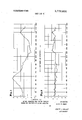
- FIG. I is aview of an embodiment of a variable resistor'illustrating the placement of electrically conductive segments.
- FIG. 2 is a sectioned view taken along the line 22 of FIG. 1.
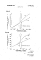
- FIG. 3 is a graph where the difference. between the resistance characteristic of a resistive element as manufactured and the resistance characteristic of a desired or-ideal resistive element is plotted.
- FIG. 4 is a graph where the difference between the resistance characteristic of a resistive element as manufactured and after trimming and the resistance characteristic of a desired or ideal resistive element is plotted.
- FIG. 5 is a graph where the difference between the voltage ratio characteristic of a resistive element as manufacturedv and the voltage ratio characteristic of a desired or ideal resistive element is plotted.
- FIG. 6 is a graph where the difference between the voltage ratio characteristic of a resistive element as manufactured and after trimming and the voltage ratio characteristic of a desired or ideal resistive element is plotted.
- FIG. 7 is a diagramatic representation of the effects of trimming on a prior art resistor.
- FIG. 8 is a diagramatic representation of the effects of trimming on an embodiment of the present invention.
- FIG. 9 is a graph comparing resistance characteristic in the vicinity of a trimming location before and after trimming on a prior art resistor.
- FIG. is a graph comparing resistance characteristic in the vicinity of a trimming location before and after trimming on a resistor of the present invention.
- FIG. 11 is a graph of the resistance differential of a resistive element as manufactured and after trimming in accordance with the prior art (without having a plurality of closely spaced electrically conductive segments).
- FIG. 12 is a graph of the resistance differential of a resistive element as manufactured and after trimming in accordance with the present invention.
- FIG. 13 is a graph where the difference between the voltage ratio characteristic of a resistive element without conductive segments and a desired or ideal voltage ratio characteristic is plotted.
- FIG. 14 is a graph where the difference between the voltage ratio characteristic of the resistive element with conductive segments and a desired or ideal voltage ratio characteristic is plotted.
- FIG. 15 is a perspective view of a potentiometer illustrating a preferred embodiment of the present invention.
- FIG. 16 is a perspective view of a portion of a potentiometer illustrating another preferred embodiment of the present invention.
- FIG. 17 is a perspective view of a portion of a potentiometer illustrating still another preferred embodiment of the present invention.
- FIG. 1 an embodiment of an adjustable resistor 20 such as those used for potentiometers.
- the resistor 20 comprises a body of electrically conductive material having a high resistance (or low conductivity), such as a resistive film 22 coated on an insulative base or substrate 24 as best seen in FIG. 2. Positioned along the resistor is a plurality of closely spaced electrically conductive segments 26 of low resistance. Two electrically conductive terminals or pads 28 and 30 are provided near each end of the resistor 20 (and extending across the resistor) and are used to connect the resistor to other circuitry and, more importantly, are used to provide an electrical potential across the resistor which establishes a potential gradient parallel to the longitudinal axis of the resistor 20.
- the spaced segments 26 extend only partially across the width of the resistor dividing the resistor into two zones, one having conductive segments, the other free of the segments.
- the segments are essentially perpendicular to the orientation of the potential gradient; stated another way, the segments 26 are positioned essentially perpendicular to imaginary current flow lines or essentially parallel to imaginary equipotential lines formed by the potential difference between pads 28 and 30. A fuller explanation will be given below when referring to FIGS. 7 and 8.
- the segments are conductively isolated from each other and from any other element of the resistor or potentiometer.
- conductively isolated it is meant that the segments are not connected in any normal fashion to conduct current to any other elements; that is, there is no electrically conductive element connecting a segment with any other element or component of the resistor or potentiometer or a system of which the resistor or potentiometer may be a part.
- an electrically conductive element or terminal 32 is provided.
- the wiper 32 is movable in a direction parallel to the orientation of the potential gradient in the zone free of the segments for allowing variability of the resistance signal derived from the resistor 20.
- the input voltage is that applied across the resistor 20 from pad 28 to pad 30 while the output voltage is measured from pad 28 to the wiper 32, for example.
- Trimming is necessary because of imperfections in material used and because of imperfections in the method of applying a resistive coating upon a substrate. As illustrated in FIG. 2, the resistive film 22 has a rough, uneven surface with some portions of the substrate 24 being coated with more film than other portions. Trimming compensates to a degree for these manufacturing and material deficiencies.
- FIGS. 3 and 4 are of resistance characteristics while FIGS. 5 and 6 are of voltage ratio characteristics.
- the X-coordinates of FIGS. 3 and 4, designated 31 and 33 respectively, refer to the distance or travel along a ring shaped resistive element similar in construction to that shown in FIG. 15.
- the Y-coordinates designated 34 and 35 in FIGS. 3 and 4, respectively, are sealed in millivolts and represent the sum difference between an ideal resistance characteristic and the actual resistance characteristic.
- the ideal resistance characteristic would be a line superimposed upon the X- coordinates 31 and 33. As can be easily seen, the resistance characteristic in FIG.
- FIGS. 5 and 6 have the same X-coordinates as FIGS. 3 and 4.
- the Y-coordinates are scale in percent and represent the difference between the actual voltage ratio and an ideal voltage ratio. As can easily be seen, the voltage ratio in untrimmed condition, FIG. 5, varies between about +0.3 to about 0.2 percent while after trimming, FIG. 6, the variation is between about +0.09 to about 0.07 percent.
- trimmings are illustrated at locations of the resistor between pairs of the segments 26.
- locations designated 34, 36 and 38 there is illustrated removal trimming; that is, a portion of the resistive film 22 has been removed, thereby reducing the cross-sectional area of the resistive film in order to increase the resistance per unit length at that section where the trimming occurs.
- removal trimming that is, a portion of the resistive film 22 has been removed, thereby reducing the cross-sectional area of the resistive film in order to increase the resistance per unit length at that section where the trimming occurs.
- 40 also positioned between a pair of the segments 26
- there is an example of the addition of electrically conductive material upon the resistive film thereby decreasing the resistance per unit length at that section where the trimming occurs. Since there are resistance changes at particular locations, total resistance of the resistor 20 changes so that the characteristic curves are altered.
- conductors and conductors of low resistance and electrically conductive segment or terminal refer, for example, to copper or silver elements which are the two most widely used conductive materials; equivalent conductive materials may also be used. More specifically, the bulk resistivity of commercially annealed copper is about 1.72 X ohm-centimeters at C, while silver is about 1.6 X 10 ohm-centimeters at 20 C. Any suitable material having a bulk resistivity of 10 to 10 ohm-centimeters will suffice.
- Terms such as material of high resistance and resistive film or materials of low conductivity refer, for example, to conductive plastics, carbon films, ceramic-metallic oxide films, metallic films or conductive ceramics. These materials have bulk resistive values of about 0.1 to 100.00 ohmcentimeters at 20 C. Any suitable material having a bulk resistivity of 10 to 10 ohm-centimeters will suffice.
- a term such as insulative refers to materials that are considered insulators, such as expoxies, phenolics and diallylphthalate. These materials have a bulk resistivity value of about 10 to 10 ohm-centimeters at C. Other materials such as glass or ceramics may be used or other suitable materials having a bulk resistivity of 10' to 10 ohm-centimeters will suffice.
- potential gradient is the rate of change of voltage per unit distance or the change in potential along the resistor created by an applied potential across the resistor; the potential gradient may be conveniently thought of as imaginary lines extending the longitudinal length of the resistor coincident the current flow lines of FIGS. 7 and 8.
- Equipotential lines are imaginary lines of equal potential disposed at substantially right angles to the potential gradient or current lines.
- resistance value refers to the actual resistance measurement between any two specific locations on the resistor.
- FIG. 7 there is illustrated an enlarged view of a portion of a resistor such as that shown in FIG. 1 absent the conductive segments 26.
- the FIG. 7 embodiment illustrates a resistive element 42 of high resistance or low conductivity material after trimming (a portion of the material has been removed at the location designated 44). Also illustrated is a rectangular area 46 representing the location of a wiper in engagement with the surface of the element. Also depicted is a series of equipotential lines 48 drawn in a generally vertical direction and a series of current flow lines 50 which are drawn generally horizontal. As mentioned, the equipotential lines and the current flow lines are a diagramatic illustration caused by an applied potential across the element 42.
- trimming may be of any desired length across the width of the element 42; additionally, the width of the trim (in a direction parallel to the longitudinal axis of the element 42) may be of any suitable dimension. The dimensions of the trimming depend upon the type of instrument used to make the removal and on the skill of the operator of the instrument.
- Another disturbing problem which is illuatrated in FIG. 7 is the broad effect caused by the trim; that is, as illustrated by the distorted equipotential lines 48, trimming at a particular location will cause a change along a far greater area of the resistor than the actual dimensions of the trimming.
- the effect of the trimming will not be restricted to that particular location but will extend a considerable distance away from the trimming. This lack of trimming localization is highly undesirable.
- FIG. 8 there is illustrated an enlarged view of a resistive element 54 such as shown in FIG. 1, including a number of closely spaced electrically conductive segments 26. There is a trimming of the high resistance material at a location designated 52. An area designated 56 is used to illustrate the engagement made between the element 54 and a wiper which is designed to move along the surface in a manner already described for the wiper in FIG. 7. Also illustrated are equipotential lines 58 and current flow lines 60 which are disposed in a perpendicular relationship to the equipotential lines 58. It is readily understood that since the conductive segment 26' is of low resistance or high conductivity, any potential difference which appears across a particular segment will be corrected so that the equipotential lines will remain essentially vertical and parallel as illustrated. That is, the segment will average the potential difference at all points along its length.
- FIGS. 9 and 10 there is a graphical demonstration of the advantage achieved by way of the present invention (FIG. 10) over the prior art (FIG. 9).
- the graph of FIG. 9 illustrates a portion of a resistance characteristic line 70 of a resistor having a structure similar to that shown in FIG. 1 absent the conductive segments 26 A trimming removal having a width of approximately 0.06 inches was made.
- Line 72 is a portion of the resistance characteristic of the resistor after trimming and quite clearly indicates, by not being parallel with line 70, that effects of the trimming extend to a distance of about 0.27 inches in a direction to the left of the trimming and more than 0.30 inches to the right of the trimming.
- FIG. 10 illustrates portions of the resistance characteristics of a resistor constructed in a manner similar to that shown in FIG. 1.
- line 74 illustrates the portion of the resistance characteristic before a trimming removal is made; while line 76 illustrates the portion of the resistance characteristic after trimming.
- the width of the trimming is about 0.06 inches. It is to be noted that the effect of the trimming extends to the left a distance of about 0.11 inches and extends to the right a distance of about 0.12 inches. Thus, trimming between a pair of conductive segments substantially localizes its effects. Predictability is also enhanced as resistance is a linear function of distance through the trimming location.
- FIG. 11 there is plotted a resistance characteristic of a resistive element in the as manufactured conditon; that is, a resistive element which was built under usual production conditions.
- the resistive element does not have any closely spaced conductive segments on it.
- the X-coordinate represents distance while the Y-coordinate is millivolts (there is a constant current input). Trimming of the resistive element occurs at three locations resulting in the three step increases in millivolt reading illustrated.
- FIG. 12 represents the resistance characteristic of a resistive element having the closely spaced conductive elements in the as-manufactured condition.
- the X and Y coordinates are identical to those of FIG. 1 1 and there is trimming of the resistive elements'in three locations as in resistive element used for the FIG. 11 graph.
- FIGS. 13 and 14 the smoothness improvement is again shown when a comparison of voltage ratio characteristic plots is made.
- FIG. 13 represents the resistive element without conductive segments
- FIG. 14 represents the resistive element with conductive segments.
- the advantages achieved could also be achieved if the electrically conductive segments were not lines but instead were a series of dots or dashes. The averaging effect on the equipotential lines would still occur so as to correct distortions. Also, it is noted that the segments may be divided in half and positioned so that the resistive element is divided into three zones, two outer zones having the spaced conductive segments in alignment and the third or central zones being free of the segments and providing a track for the wiper.
- Resistive elements having conductors crossing the elements have been made in the past. However, there has never been a recognition of the advantages of closely spacing electrically conductive segments.
- the conductors of the prior art were incorporated for completely different purposes than those set forth herein and thus were structurally different.
- the conductors were connected to terminals, commonly called taps, so that their signals or output could be made available to other electrical circuitry.
- the purpose of having taps along the length of the resistor was to make the resistive element more versatile by providing an apparent change in the efi'ective resistance by means of shunt circuitry between the taps. Taps are generally not closely spaced as is required and desirable in the preferred embodiments of the present invention.
- conductors which were connected to external or other circuitry and expected to provide informational signals efforts were made to prevent disturbances about the conductors. Since trimming causes distortions as explained above, it was likely in the prior art that trimming took place away from the conductors.
- the method of manufacturing a resistor of the preferred type comprises the steps of providing a body of high resistance material, such as resistive film 22, FIG. 1, placing a plurality of closely spaced electrically conductive segments of low resistance such as segment 26 so that the segments are essentially perpendicular to the orientation of a potential gradient of an applied electrical potential.
- the resistor may be manufactured by providing a substrate of insulative material such as an epoxy, diayllylphthalate, phenol, glass or any other commonly used insulative material.
- the purpose of insulating material is to support a resistive material and electrically separate the resistive element of a resistor from a surrounding environment such as a metal housing.
- the substrates are molded to a desired predetermined shape.
- a layer of film of resistive material is applied to the substrate by any suitable means.
- conductive resistive films include conductive plastics, carbon films (emulsion of carbon) and ceramic-metallic I films may be applied in any suitable fashion such as by spraying, dipping, painting, silk screening, vacuum evaporating or sputtering, all of which are well known methods.
- a plurality of conductive segments of low resistance material such as silver, copper or nickel, is applied by spraying, painting or silk screening and may be applied before, during or after the resistive element is applied, depending upon the choice of material. The sequence of application of the segments and the resistive film is unimportant.
- the resistor is usually machined and cured and provided with terminals for suitably connecting the resistor to other circuit elements (the terminals could be molded into location during the molding of the base).
- the resistor of FIG. 1 comprises a glass substrate supporting a deposit of high resistance conductive film which in turn supports a plurality of deposited silver segments.
- the length of the resistor between the two outermost silver pads is approximately 6.5 inches while the width of the resistor is approximately 0.375 inches.
- the silver segments are 0.006 inches thick with a spacing of about 0.060 between adjacent segments. Each segment extended approximately 0.187 inches across the width of the resistor. It is noted that the ratio of the spacing between segments to the width of a segment is about to l.
- a cylindrical potentiometer which is comprised of a moldable plastic insulative substrate 100 in the shape of a hollow cylinder with an outer surface 102 and an inner surface 104.
- a resistive film 106 which provides the resistive element of the potentiometer.
- Deposited upon the resistive film is a plurality of segments 108.
- Two pads, 110 and 112 are connected to terminals 114 and 116 respectively, to allow a potential difference to be applied across the film 106.
- FIG. embodiment is analogous to the embodiment shown in FIG. 1. Trimming is illustrated at two locations designated 124 and 126.
- FIG. 16 illustrates a radial or disc resistive element for a potentiometer which is comprised of a cylindrical insulated substrate 130 having two end surfaces one of which supports a conductive resistive film 132 upon which a plurality of electrically conductive segments 134 is deposited.
- the resistive film 132 is di vided into two zones, a first or outer zone containing segments 134 and an inner zone designated 136 which provides the track for a rotatable wiper (not shown).
- two pads, 140 and 142 are provided for establishing a potential differential along the resistive element 132.
- FIG. 17 illustrates a preferred embodiment in which the resistive element 150 is applied in a helical fashion to a cylindrical base 152 so as to form what is commonly called a multi-turn resistive element.
- the resistive element has a plurality of closely spaced electrical conductors 154 which occupy a first zone on the film while a second zone of the film is provided for the movable wiper (not shown).
- resistive element having a plurality of closely spaced segments may take a variety of different forms as clearly indicated by the various embodiments, FIGS. 1, 15, 16 and 17.
- the method of altering the resistance characteristic of an element of high resistance comprises the steps of providing an element of high resistance having a plurality of closely spaced electrically conductive segments of low resistance where the segments are effectively conductively isolated from each other and from any other elements.
- Resistance value of the element is controllably increased by removing a portion of the high resistance material between a pair of the segments.
- the resistance value of the element may be decreased by adding conductive material to the element between a pair of the segments. It is understood that a combination of removing and adding material to various portions of the high resistance element may be necessary to provide the desired resistance and/or voltage ratio characteristics.
- the trimming method comprises initially comparing the desired resistance and/or voltage ratio characteristic and the actual characteristic and adjusting the actual characteristic by trimming as required. Trimming is done by removing or adding material as explained above.
- the removal trimming may be easily accomplished with a burr device, a small rotary cutting tool similar to that used by dentists.
- Other removal devices include abrasive jets, pulsed liquid jets or lasers.
- Adding material may be accomplished by the same process used to deposit the conductive segments on the resistive material. It is quite clear that an entire segment or a portion of a segment may be removed if it is found necessary in order to achieve the desired resistance or voltage ratio characteristic (see location 38, FIG. 1 for example). As long as the removed portion still lies between any two of the segments, the distortion of the potential gradient found in the prior art will be greatly reduced.
- added conductive material may be used to bridge two adjacent segments in order to substantially lower the resistance of the resistive element. Once again, the distortions usually produced by trimming are greatly reduced by the proximity of other segments.
- an electrically conductive element for making conductive contact with a first area of the high resistance material, said conductive element and said high resistance material being movable relative one another along said first area;
- c. means for connecting said high resistance material and said conductive element to external electrical circuitry; and aplurality of closely spaced electrically conductive segments of low resistance positioned along the high resistance material outside of said first area so as to be essentially perpendicular to the orientation of a potential gradient capable of being established along the high resistance material, said spaced conductive segments being effectively conductively isolated from each other, from other elements of said variable resistor and from elements external to the variable resistor;
- said high resistance material having a varied thickness between two of said conductive segments for distorting said potential gradient therebetween and for localizing changes in said potential gradient to an extension of the spacing between said two closely spaced conductive segments in said first area of the high resistance material.
- variable resistor as claimed in claim -1 wherein a portion of said high resistance material between two of said conductive segments has an appreciably reduced amount of said high resistance material as compared with other portions of said high resistance material for increasing the resistance of said high resistance material.
- a variable resistor as claimed in claim 2 wherein another portion of said high resistance material between two of said conductive segments has an amount of electrically conductive material for decreasing the resistance of said high resistance material.
- variable resistor as claimed in claim 1 wherein a portion of said high resistance material between two of said conductive segments has an amount of electrically conductive material for decreasing the resistance of said high resistance material.
- said high resistance material having a varied thickness between respective pairs of said conductive segments for distorting said potential gradient between said conductive segments within said first part and for substantially limiting said distortion of said potential gradient to an extension of the spacing between said conductive segments in said second part.
- a method of altering the resistance characteristic of an electrically conductive element of high resistance where the alteration results in a change in the resistance of said element comprising the steps a. providing an electrically conductive element of high resistance material;
Landscapes
- Engineering & Computer Science (AREA)
- Microelectronics & Electronic Packaging (AREA)
- Manufacturing & Machinery (AREA)
- Apparatuses And Processes For Manufacturing Resistors (AREA)
Abstract
An improved resistor such as found in potentiometers and rheostats is disclosed as well as the method of manufacturing such resistors and the method of trimming such resistors. A preferred embodiment of the resistor is structured with a resistive film deposited upon a substrate. A number of closely spaced electrically conductive segments are deposited upon the resistive film for reducing electrical distortion caused by trimming and manufacturing anomalies.
Description
United States Patent Owen 1 Nov. 13, 1973 [54] RESISTOR AND METHOD OF MAKING 2,500,605 3/1950 Lange et al. 338/195 X AND TRIMMING SAME 2,632,831 3/1953 Pritikin et al. 3,379,567 4/1968 Wright 338/195 X Inventor: Alex B. Owen, Wallingford, Pa.
[73] Assignee: Litton Systems, Inc., Beverly Hills, Primary Examiner Robert schflffer C lifl Assistant ExaminerGerald P. Tolin Attorney-Alan C. Rose, Ronald W. Reagin and Jo- [22] Filed: Aug. 12, 1969 Seph Golant [21] Appl. No.: 849,332 7 [57] ABSTRACT 52 us. Cl. 338/195, 338/308 An improved resistor such as found in Potentiometers [51] Int. Cl 1101c 9/02 and Theostats is disclosed as a the method of 53 Field f Search 33 /75 9 91 manufacturing such resistors and the method of trim- 33g 2 138, 39 40 4 5 307 ming such resistors. A preferred embodiment of the 30 309 333 334 13; 29 10 20 resistor is structured with a resistive film deposited upon a substrate. A number of closely spaced electri- [56] References Cited cally conductive segments are deposited upon the re- UNITED STATES PATENTS sistive film for reducing electrical distortion caused by trimming and manufacturing anomalies. 1,918,050 7/1933 Mattem 338/ X 10 Claims, 17 Drawing Figures 34 3e 38 W "I MW i l FE J 3o 28 22 RESISTOR AND METHODOF MAKING AND TRIMMING SAME BACKGROUND OF THE INVENTION.
Trimmable resistors are well known and. have beenv used. as elements in such devices as rheostats and. potentiometers. The word-trimmable refers to the resistors capabilityof having. its resistance. and voltage characteristics altered by. the removal of a portion or portions of the resistancematerialof the resistor was to effect a reduced crosssectional area in order to increase resistance. value and/or alteredby. the addition.
of low resistance material to a portion or portions of a resistor in order to decrease resistance value.
Generally, allresistorsare manufactured to-have desired. resistance. and/or voltage characteristics in orderto fulfill a particular application. The resistance char acteristic of an element may be illustrated as agraphical curve developed as resistance value of the element is plotted against distance or displacement along the element. The resistance characteristic. may also be thought of as the relationship of: output: compared to contact element or wiper travel. The voltage ratio characteristic may be defined as the. ratio of the voltage between the wiper and. a designated reference point,
. usually one of the end. terminals, to theinput. voltage,
usually that voltage between the two end terminals plotted against distance or travel. of the wi'per. Because the manufacturing of a resistor is not an exact art, especially the manufacturing of a resistor of the film type, (a type having aninsulative base with a coating of resistive material) it. is necessary to have some method of adjusting the actual characteristics of the resistor tothe. desired characteristics. Trimming is a method commonly used to alter the characteristics. However, trimming itself is not very accurate because of the many parameters affecting the characteristics of a resistor. For example, if a portionof the resistive tilmof a film-type resistor was removed there would be a change of resistance value per unit length at that section of the resistor from which the portion istaken. However, the change would occur over a. relatively wide section along the resister, as compared with the length and width of the trimming. Thus, removing a portion having a width of 0.06 inches may affect resistance value along a length on the resistor of more than 0.5 inches. This phenomenon will hereinafter be referred to as the. degree of localization of trimming upon the characteristics of a resistor.
Additionally, the greater the length affected by trimming, the greater the difficulty in predictability of the actual change in resistance values at. any particular location along the length. Thus, at a specific distance away from the trim itwill not be known to what degree a change has occurred.
Another problem is apparent when plotting the characteristics of a film-type resistor on paper. If resistance value is plottedagainst distance the curve developed is jagged; this is indicative of local irregularities or anomalies in the resistive film. The same jagged curve appearswhen plotting the voltage characteristic. The jaggedness, of course, frustrates close tolerance trimming.
SUMMARY OF THE INVENTION The present invention moves a long. way toward alleviating the above mentioned problems by providing a variable resistor with the ability to have its characteristic easily changed comprising in combination an electrically. conductive material having ahigh resistance; an electrically conductive element for making electrical. contact with the highresistancematerial, the conductive element and the high resistance material being movable relative one another; means for connecting the high resistance material and the conductive element to external electrical circuitry; and'a plurality of closely spaced electrically conductive segments of low resistance positioned along the highresistance material so as to be generally perpendicular to the orientation of a, potential gradient capable of being established along the high resistance material, theconductive segments being effectively conductively isolated from each other, from other elementsof the variable resistor and fromelements external to the variable resistor.
Additionally, the present invention includes a method of manufacturing such a variable resistor and the method of trimming the resistor.
An object of the present invention is to provide a variable resistor having a capability of localizing the effect of trimming and having the capability of reducing error'due to manufacturing and/or material anomalies.
Another object of the invention is to provide a variable resistor whose trimming may be achieved quickly and economically, resulting in an improved apparatus capable of providing more accurate output signals.
BRIEF DESCRIPTION OF THE DRAWINGS FIG. I is aview of an embodiment of a variable resistor'illustrating the placement of electrically conductive segments.
FIG. 2 is a sectioned view taken along the line 22 of FIG. 1.
FIG. 3 is a graph where the difference. between the resistance characteristic of a resistive element as manufactured and the resistance characteristic of a desired or-ideal resistive element is plotted.
FIG. 4 is a graph where the difference between the resistance characteristic of a resistive element as manufactured and after trimming and the resistance characteristic of a desired or ideal resistive element is plotted.
FIG. 5 is a graph where the difference between the voltage ratio characteristic of a resistive element as manufacturedv and the voltage ratio characteristic of a desired or ideal resistive element is plotted.
FIG. 6 is a graph where the difference between the voltage ratio characteristic of a resistive element as manufactured and after trimming and the voltage ratio characteristic of a desired or ideal resistive element is plotted.
FIG. 7 is a diagramatic representation of the effects of trimming on a prior art resistor.
FIG. 8 is a diagramatic representation of the effects of trimming on an embodiment of the present invention.
FIG. 9 is a graph comparing resistance characteristic in the vicinity of a trimming location before and after trimming on a prior art resistor.
FIG. is a graph comparing resistance characteristic in the vicinity of a trimming location before and after trimming on a resistor of the present invention.
FIG. 11 is a graph of the resistance differential of a resistive element as manufactured and after trimming in accordance with the prior art (without having a plurality of closely spaced electrically conductive segments).
FIG. 12 is a graph of the resistance differential of a resistive element as manufactured and after trimming in accordance with the present invention.
FIG. 13 is a graph where the difference between the voltage ratio characteristic of a resistive element without conductive segments and a desired or ideal voltage ratio characteristic is plotted.
FIG. 14 is a graph where the difference between the voltage ratio characteristic of the resistive element with conductive segments and a desired or ideal voltage ratio characteristic is plotted.
FIG. 15 is a perspective view of a potentiometer illustrating a preferred embodiment of the present invention.
FIG. 16 is a perspective view of a portion of a potentiometer illustrating another preferred embodiment of the present invention.
FIG. 17 is a perspective view of a portion of a potentiometer illustrating still another preferred embodiment of the present invention.
DESCRIPTION OF THE PREFERRED EMBODIMENTS Referring to the Drawings wherein like numerals designate like or corresponding parts throughout the several views, there is illustrated in FIG. 1 an embodiment of an adjustable resistor 20 such as those used for potentiometers.
The resistor 20 comprises a body of electrically conductive material having a high resistance (or low conductivity), such as a resistive film 22 coated on an insulative base or substrate 24 as best seen in FIG. 2. Positioned along the resistor is a plurality of closely spaced electrically conductive segments 26 of low resistance. Two electrically conductive terminals or pads 28 and 30 are provided near each end of the resistor 20 (and extending across the resistor) and are used to connect the resistor to other circuitry and, more importantly, are used to provide an electrical potential across the resistor which establishes a potential gradient parallel to the longitudinal axis of the resistor 20. The spaced segments 26 extend only partially across the width of the resistor dividing the resistor into two zones, one having conductive segments, the other free of the segments. The segments are essentially perpendicular to the orientation of the potential gradient; stated another way, the segments 26 are positioned essentially perpendicular to imaginary current flow lines or essentially parallel to imaginary equipotential lines formed by the potential difference between pads 28 and 30. A fuller explanation will be given below when referring to FIGS. 7 and 8.
It is to be noted that the segments are conductively isolated from each other and from any other element of the resistor or potentiometer. By the term conductively isolated it is meant that the segments are not connected in any normal fashion to conduct current to any other elements; that is, there is no electrically conductive element connecting a segment with any other element or component of the resistor or potentiometer or a system of which the resistor or potentiometer may be a part.
To complete the basic elements of a potentiometer, an electrically conductive element or terminal 32, more commonly called the wiper", is provided. The wiper 32 is movable in a direction parallel to the orientation of the potential gradient in the zone free of the segments for allowing variability of the resistance signal derived from the resistor 20. In a potentiometer the input voltage is that applied across the resistor 20 from pad 28 to pad 30 while the output voltage is measured from pad 28 to the wiper 32, for example.
Trimming is necessary because of imperfections in material used and because of imperfections in the method of applying a resistive coating upon a substrate. As illustrated in FIG. 2, the resistive film 22 has a rough, uneven surface with some portions of the substrate 24 being coated with more film than other portions. Trimming compensates to a degree for these manufacturing and material deficiencies.
Referring now to FIGS. 3 and 4 and to FIGS. 5 and 6, comparisons are illustrated of the characteristics of a resistive element as manufactured and then after trimming. FIGS. 3 and 4 are of resistance characteristics while FIGS. 5 and 6 are of voltage ratio characteristics. The X-coordinates of FIGS. 3 and 4, designated 31 and 33 respectively, refer to the distance or travel along a ring shaped resistive element similar in construction to that shown in FIG. 15. The Y-coordinates designated 34 and 35 in FIGS. 3 and 4, respectively, are sealed in millivolts and represent the sum difference between an ideal resistance characteristic and the actual resistance characteristic. The ideal resistance characteristic would be a line superimposed upon the X- coordinates 31 and 33. As can be easily seen, the resistance characteristic in FIG. 3, when a constant current is applied, varies between about +8 millivolts and about 9 millivolts in the untrimmed condition. After trimming the variation is between about +2 and about 2 millivolts. FIGS. 5 and 6 have the same X-coordinates as FIGS. 3 and 4. The Y-coordinates are scale in percent and represent the difference between the actual voltage ratio and an ideal voltage ratio. As can easily be seen, the voltage ratio in untrimmed condition, FIG. 5, varies between about +0.3 to about 0.2 percent while after trimming, FIG. 6, the variation is between about +0.09 to about 0.07 percent.
Referring again to FIG. 1, trimmings are illustrated at locations of the resistor between pairs of the segments 26. For example, at locations designated 34, 36 and 38 there is illustrated removal trimming; that is, a portion of the resistive film 22 has been removed, thereby reducing the cross-sectional area of the resistive film in order to increase the resistance per unit length at that section where the trimming occurs. In another location on the resistor, designated 40, also positioned between a pair of the segments 26, there is an example of the addition of electrically conductive material upon the resistive film, thereby decreasing the resistance per unit length at that section where the trimming occurs. Since there are resistance changes at particular locations, total resistance of the resistor 20 changes so that the characteristic curves are altered.
In the use of terms in the present Specification it will be endeavored to use terms as they are normally employed by persons working in the field of the present invention. Thus terms such as conductors and conductors of low resistance and electrically conductive segment or terminal refer, for example, to copper or silver elements which are the two most widely used conductive materials; equivalent conductive materials may also be used. More specifically, the bulk resistivity of commercially annealed copper is about 1.72 X ohm-centimeters at C, while silver is about 1.6 X 10 ohm-centimeters at 20 C. Any suitable material having a bulk resistivity of 10 to 10 ohm-centimeters will suffice. Terms such as material of high resistance and resistive film or materials of low conductivity refer, for example, to conductive plastics, carbon films, ceramic-metallic oxide films, metallic films or conductive ceramics. These materials have bulk resistive values of about 0.1 to 100.00 ohmcentimeters at 20 C. Any suitable material having a bulk resistivity of 10 to 10 ohm-centimeters will suffice. A term such as insulative refers to materials that are considered insulators, such as expoxies, phenolics and diallylphthalate. These materials have a bulk resistivity value of about 10 to 10 ohm-centimeters at C. Other materials such as glass or ceramics may be used or other suitable materials having a bulk resistivity of 10' to 10 ohm-centimeters will suffice.
The term potential gradient is the rate of change of voltage per unit distance or the change in potential along the resistor created by an applied potential across the resistor; the potential gradient may be conveniently thought of as imaginary lines extending the longitudinal length of the resistor coincident the current flow lines of FIGS. 7 and 8. Equipotential lines are imaginary lines of equal potential disposed at substantially right angles to the potential gradient or current lines.
The term resistance value refers to the actual resistance measurement between any two specific locations on the resistor.
Referring now to FIG. 7, there is illustrated an enlarged view of a portion of a resistor such as that shown in FIG. 1 absent the conductive segments 26. The FIG. 7 embodiment illustrates a resistive element 42 of high resistance or low conductivity material after trimming (a portion of the material has been removed at the location designated 44). Also illustrated is a rectangular area 46 representing the location of a wiper in engagement with the surface of the element. Also depicted is a series of equipotential lines 48 drawn in a generally vertical direction and a series of current flow lines 50 which are drawn generally horizontal. As mentioned, the equipotential lines and the current flow lines are a diagramatic illustration caused by an applied potential across the element 42. The discussion to follow is based in part on two papers presented at the Precision Potentiometer Manufacturers Association Technical Symposium, Aug. 19, 1963 by Mr. Richard D. Ward and by Dr. Ronald B. Goldner titled, respectively, Conductive Plastic Potentiometer Linearity Correction and Curvilinear Squares As a Method for Assisting in the Design of Linear and Non-Linear Potentiometers.
As the wiper moves along parallel to the current flow lines, it is desirable to have the equipotential lines in a perpendicular orientation so that clear signals are transmitted by the wiper. However, trimming at location 44 distorts the orientation of the equipotential lines and causes the wiper, as illustrated by the area 46, to intersect simultaneously equipotential lines which are at different potential values. By virtue of the potential difference along the wiper there is a current flow set up in the head of the wiper in order to equalize the potential along the wiper. The introduction of this extraneous current is very undesirable as it will superimpose upon the signal at that location to give an erroneous output.
It is to be noted that trimming may be of any desired length across the width of the element 42; additionally, the width of the trim (in a direction parallel to the longitudinal axis of the element 42) may be of any suitable dimension. The dimensions of the trimming depend upon the type of instrument used to make the removal and on the skill of the operator of the instrument.
Another disturbing problem which is illuatrated in FIG. 7 is the broad effect caused by the trim; that is, as illustrated by the distorted equipotential lines 48, trimming at a particular location will cause a change along a far greater area of the resistor than the actual dimensions of the trimming. Thus, if a trimming is made to offset a particular anomaly at a particular location of the element 42, the effect of the trimming will not be restricted to that particular location but will extend a considerable distance away from the trimming. This lack of trimming localization is highly undesirable.
Referring now to FIG. 8, there is illustrated an enlarged view of a resistive element 54 such as shown in FIG. 1, including a number of closely spaced electrically conductive segments 26. There is a trimming of the high resistance material at a location designated 52. An area designated 56 is used to illustrate the engagement made between the element 54 and a wiper which is designed to move along the surface in a manner already described for the wiper in FIG. 7. Also illustrated are equipotential lines 58 and current flow lines 60 which are disposed in a perpendicular relationship to the equipotential lines 58. It is readily understood that since the conductive segment 26' is of low resistance or high conductivity, any potential difference which appears across a particular segment will be corrected so that the equipotential lines will remain essentially vertical and parallel as illustrated. That is, the segment will average the potential difference at all points along its length.
When trimming becomes necessary it has been found that if the removal or addition of material occurs between a pair of the conductive segments (see location 52), the disturbance caused by trimming is relatively localized since the conductive segments will act to correct the distortion which appears. Thus, any distortion of the equipotential and current flow lines is generally limited to that part of the element located between a pair of conductive segments. At the same time, the localization of the trimming allows an increased predictability of the change of resistance value at different points along the element 54. Finally, there is a marked reduction or elimination of the potential difference appearing across the wiper so that superimposition of signals is reduced or eliminated. It is to be understood that FIGS. 7 and 8 are not drawn to scale but are used for illustrative purposes of theory only.
It would appear desirable to have the conductive segments 26 thin, closely spaced and extending fully across the width of the resistor. However, very practical limitations exist to these three desired goals. There is presently a limit to the narrowness of the conductive segment, using today's economical methods of applying the segments to the resistor. Secondly, if the conductor material is too closely spaced so as to occupy too large an area relative the resistive material, there will be a shunting effect which will destroy the resistance characteristic of the resistor. Third, though it is possible to have the segment extend fully across the resistor, it is not generally desirable because there is a slight signal disturbance created when the wiper comes into contact with any of the segments.
Referring now to FIGS. 9 and 10 there is a graphical demonstration of the advantage achieved by way of the present invention (FIG. 10) over the prior art (FIG. 9). The graph of FIG. 9 illustrates a portion of a resistance characteristic line 70 of a resistor having a structure similar to that shown in FIG. 1 absent the conductive segments 26 A trimming removal having a width of approximately 0.06 inches was made. Line 72 is a portion of the resistance characteristic of the resistor after trimming and quite clearly indicates, by not being parallel with line 70, that effects of the trimming extend to a distance of about 0.27 inches in a direction to the left of the trimming and more than 0.30 inches to the right of the trimming.
FIG. 10 illustrates portions of the resistance characteristics of a resistor constructed in a manner similar to that shown in FIG. 1. Here line 74 illustrates the portion of the resistance characteristic before a trimming removal is made; while line 76 illustrates the portion of the resistance characteristic after trimming. The width of the trimming is about 0.06 inches. It is to be noted that the effect of the trimming extends to the left a distance of about 0.11 inches and extends to the right a distance of about 0.12 inches. Thus, trimming between a pair of conductive segments substantially localizes its effects. Predictability is also enhanced as resistance is a linear function of distance through the trimming location. (Note linearity of line 76 through the trimming location.) Similar tests have been conducted where the trimming consisted of an addition of conductive material to the resistor in order to cause a localized decrease in resistance value. The localization effect due to the conductive segments was again found to be substantially improved over the resistor of the prior art.
Referring now to FIG. 11 there is plotted a resistance characteristic of a resistive element in the as manufactured conditon; that is, a resistive element which was built under usual production conditions. The resistive element does not have any closely spaced conductive segments on it. Once again the X-coordinate represents distance while the Y-coordinate is millivolts (there is a constant current input). Trimming of the resistive element occurs at three locations resulting in the three step increases in millivolt reading illustrated. FIG. 12 represents the resistance characteristic of a resistive element having the closely spaced conductive elements in the as-manufactured condition. The X and Y coordinates are identical to those of FIG. 1 1 and there is trimming of the resistive elements'in three locations as in resistive element used for the FIG. 11 graph.
Comparison of the two plots clearly illustrates the smoothness of the FIG. 12 plot. During normal production, anomalies appear in the resistive element to distort the equipotential lines. Use of conductive segments greatly reduces the distortion so as 'to be negligible. Hence, signal accuracy is enhanced especially in those sections of the resistive element where trimming has occurred.
Referring now to FIGS. 13 and 14, the smoothness improvement is again shown when a comparison of voltage ratio characteristic plots is made. FIG. 13 represents the resistive element without conductive segments, while FIG. 14 represents the resistive element with conductive segments.
It is to be noted that the advantages achieved could also be achieved if the electrically conductive segments were not lines but instead were a series of dots or dashes. The averaging effect on the equipotential lines would still occur so as to correct distortions. Also, it is noted that the segments may be divided in half and positioned so that the resistive element is divided into three zones, two outer zones having the spaced conductive segments in alignment and the third or central zones being free of the segments and providing a track for the wiper.
Resistive elements having conductors crossing the elements have been made in the past. However, there has never been a recognition of the advantages of closely spacing electrically conductive segments. The conductors of the prior art were incorporated for completely different purposes than those set forth herein and thus were structurally different. The conductors were connected to terminals, commonly called taps, so that their signals or output could be made available to other electrical circuitry. The purpose of having taps along the length of the resistor was to make the resistive element more versatile by providing an apparent change in the efi'ective resistance by means of shunt circuitry between the taps. Taps are generally not closely spaced as is required and desirable in the preferred embodiments of the present invention. Additionally, by using conductors which were connected to external or other circuitry and expected to provide informational signals efforts were made to prevent disturbances about the conductors. Since trimming causes distortions as explained above, it was likely in the prior art that trimming took place away from the conductors.
Method of Manufacture The method of manufacturing a resistor of the preferred type comprises the steps of providing a body of high resistance material, such as resistive film 22, FIG. 1, placing a plurality of closely spaced electrically conductive segments of low resistance such as segment 26 so that the segments are essentially perpendicular to the orientation of a potential gradient of an applied electrical potential. In more detail, the resistor may be manufactured by providing a substrate of insulative material such as an epoxy, diayllylphthalate, phenol, glass or any other commonly used insulative material. The purpose of insulating material is to support a resistive material and electrically separate the resistive element of a resistor from a surrounding environment such as a metal housing. Generally the substrates are molded to a desired predetermined shape. Next, a layer of film of resistive material (resistive film) is applied to the substrate by any suitable means. For example, conductive resistive films include conductive plastics, carbon films (emulsion of carbon) and ceramic-metallic I films may be applied in any suitable fashion such as by spraying, dipping, painting, silk screening, vacuum evaporating or sputtering, all of which are well known methods. In addition, a plurality of conductive segments of low resistance material such as silver, copper or nickel, is applied by spraying, painting or silk screening and may be applied before, during or after the resistive element is applied, depending upon the choice of material. The sequence of application of the segments and the resistive film is unimportant.
After the molding and deposition of resistive films on the substrate, the resistor is usually machined and cured and provided with terminals for suitably connecting the resistor to other circuit elements (the terminals could be molded into location during the molding of the base).
The resistor of FIG. 1 comprises a glass substrate supporting a deposit of high resistance conductive film which in turn supports a plurality of deposited silver segments. The length of the resistor between the two outermost silver pads is approximately 6.5 inches while the width of the resistor is approximately 0.375 inches. The silver segments are 0.006 inches thick with a spacing of about 0.060 between adjacent segments. Each segment extended approximately 0.187 inches across the width of the resistor. It is noted that the ratio of the spacing between segments to the width of a segment is about to l.
Referringnow to FIG. 15, there is illustrated a cylindrical potentiometer which is comprised of a moldable plastic insulative substrate 100 in the shape of a hollow cylinder with an outer surface 102 and an inner surface 104. Deposited upon the inner surface 104 isa resistive film 106 which provides the resistive element of the potentiometer. Deposited upon the resistive film is a plurality of segments 108. Two pads, 110 and 112, are connected to terminals 114 and 116 respectively, to allow a potential difference to be applied across the film 106.
Mechanically connected to an electrically isolated rotatable shaft 120 is a wiper 122 which moves along the resister element from one of the pads to the other. The wiper is connected to a third terminal 118. In operation, the FIG. embodiment is analogous to the embodiment shown in FIG. 1. Trimming is illustrated at two locations designated 124 and 126.
Referring now to FIGS. 16 and 17, there are illustrated two other preferred embodiments of the present invention. FIG. 16 illustrates a radial or disc resistive element for a potentiometer which is comprised of a cylindrical insulated substrate 130 having two end surfaces one of which supports a conductive resistive film 132 upon which a plurality of electrically conductive segments 134 is deposited. The resistive film 132 is di vided into two zones, a first or outer zone containing segments 134 and an inner zone designated 136 which provides the track for a rotatable wiper (not shown). Once again, two pads, 140 and 142 are provided for establishing a potential differential along the resistive element 132.
FIG. 17 illustrates a preferred embodiment in which the resistive element 150 is applied in a helical fashion to a cylindrical base 152 so as to form what is commonly called a multi-turn resistive element. Once again, the resistive element has a plurality of closely spaced electrical conductors 154 which occupy a first zone on the film while a second zone of the film is provided for the movable wiper (not shown).
It is to be clearly understood that the resistive element having a plurality of closely spaced segments may take a variety of different forms as clearly indicated by the various embodiments, FIGS. 1, 15, 16 and 17. The
invention is not to be limited to those preferred embodiments used for illustration in the Drawings.
Method of Trimming The method of altering the resistance characteristic of an element of high resistance comprises the steps of providing an element of high resistance having a plurality of closely spaced electrically conductive segments of low resistance where the segments are effectively conductively isolated from each other and from any other elements. Resistance value of the element is controllably increased by removing a portion of the high resistance material between a pair of the segments. The resistance value of the element may be decreased by adding conductive material to the element between a pair of the segments. It is understood that a combination of removing and adding material to various portions of the high resistance element may be necessary to provide the desired resistance and/or voltage ratio characteristics.
In more detail, the trimming method comprises initially comparing the desired resistance and/or voltage ratio characteristic and the actual characteristic and adjusting the actual characteristic by trimming as required. Trimming is done by removing or adding material as explained above.
The removal trimming may be easily accomplished with a burr device, a small rotary cutting tool similar to that used by dentists. Other removal devices include abrasive jets, pulsed liquid jets or lasers. Adding material may be accomplished by the same process used to deposit the conductive segments on the resistive material. It is quite clear that an entire segment or a portion of a segment may be removed if it is found necessary in order to achieve the desired resistance or voltage ratio characteristic (see location 38, FIG. 1 for example). As long as the removed portion still lies between any two of the segments, the distortion of the potential gradient found in the prior art will be greatly reduced. In a like manner, added conductive material may be used to bridge two adjacent segments in order to substantially lower the resistance of the resistive element. Once again, the distortions usually produced by trimming are greatly reduced by the proximity of other segments.
What is claimed is:
1. A variable resistor with the ability to have its characteristic easily changed comprising in combination:
a. an electrically conductive material having a high resistance;
b. an electrically conductive element for making conductive contact with a first area of the high resistance material, said conductive element and said high resistance material being movable relative one another along said first area;
c. means for connecting said high resistance material and said conductive element to external electrical circuitry; and aplurality of closely spaced electrically conductive segments of low resistance positioned along the high resistance material outside of said first area so as to be essentially perpendicular to the orientation of a potential gradient capable of being established along the high resistance material, said spaced conductive segments being effectively conductively isolated from each other, from other elements of said variable resistor and from elements external to the variable resistor;
e. said high resistance material having a varied thickness between two of said conductive segments for distorting said potential gradient therebetween and for localizing changes in said potential gradient to an extension of the spacing between said two closely spaced conductive segments in said first area of the high resistance material.
2. A variable resistor as claimed in claim -1 wherein a portion of said high resistance material between two of said conductive segments has an appreciably reduced amount of said high resistance material as compared with other portions of said high resistance material for increasing the resistance of said high resistance material.
3. A variable resistor as claimed in claim 2 wherein another portion of said high resistance material between two of said conductive segments has an amount of electrically conductive material for decreasing the resistance of said high resistance material.
4. A variable resistor as claimed in claim 1 wherein a portion of said high resistance material between two of said conductive segments has an amount of electrically conductive material for decreasing the resistance of said high resistance material.
5. An electrically conductive material of high resistance with the ability to have its characteristic easily changed comprising:
a. a plurality of closely spaced electrically conductive segments of low resistance located within a first part of the high resistance material so as to be essentially perpendicular to the orientation of a potential gradient of an applicable electrical potential and as to define a second part of said high resistance material free of said conductive segments b. said conductive segments being effectively conductively isolated from each other by said high resistance material, and
c. said high resistance material having a varied thickness between respective pairs of said conductive segments for distorting said potential gradient between said conductive segments within said first part and for substantially limiting said distortion of said potential gradient to an extension of the spacing between said conductive segments in said second part.
6. An apparatus as claimed in claim 5 wherein said varied thickness of said high resistance material between respective pairs of said conductive segments has an appreciably reduced thickness of said high resistance material as compared to other portions of said high resistance material for increasing the resistance of said high resistance material.
7. An apparatus as claimed in claim 6 wherein an electrically conductive material is added to said high resistance material between other respective pairs of said conductive segments for decreasing the resistance of said high resistance material.
8. A method of manufacturing an electrically conductive element of high resistance with the ability to have its characteristic easily changed comprising the steps of:
a. providing an electrically conductive material of high resistance;
b. placing a plurality of closely spaced electrically conductive segments of low resistance in contact with said high resistance material, said conductors being placed so as to be essentially perpendicular to the orientation of a potential gradient of an applied electrical potential difference, and said conductive segments being positioned so as to be effectively conductively isolated from each other;
c. measuring the resistance of said high resistance element by directly contacting said element and sensing said applied electrical potential at said point of contact without contacting said closely spaced electrically conductive segments;
d. removing portions of said high resistance material from between said closely spaced electrically conductive segments for increasing the measured resistance of said high resistance conductive element; and
e. adding high resistance material between said closely spaced electrically conductive segments for decreasing the measured resistance of said high resistance conductive element, thereby easily changing characteristics of said element.
9. A method as claimed in claim 8 wherein said layer of high resistance material is a conductive film coated upon an electrically insulative substrate, and additionally comprising the steps of:
forming said film in two zones;
positioning the conductive segments in parallel alignment in one of said zones while the second of said zones is provided to make contact with a movable electrically conductive element.
10. A method of altering the resistance characteristic of an electrically conductive element of high resistance where the alteration results in a change in the resistance of said element, the method comprising the steps a. providing an electrically conductive element of high resistance material;
b. placing a plurality of equally spaced electrically conductive segments of low resistance on said electrically conductive element;
c. arranging said equally spaced conductive segments so as to be essentially perpendicular to the orientation of a potential gradient of an applied electrical potential, said conductive segments being so arranged as to be effectively conductively isolated from each other and from other elements;
d. contacting said electrically conductive element with a contact element to measure said resistance characteristic thereof; and
e. altering a section of said high resistance material between two of said equally spaced conductive segments so that said sections has an appreciably changed amount of resistive material causing a variation in the resistance of said section as compared with other equal sections of said high resistance material.
Claims (10)
1. A variable resistor with the ability to have its characteristic easily changed comprising in combination: a. an electrically conductive material having a high resistance; b. an electrically conductive element for making conductive contact with a first area of the high resistance material, said conductive element and said high resistance material being movable relative one another along said first area; c. means for connecting said high resistance material and said conductive element to external electrical circuitry; and d. a plurality of closely spaced electrically conductive segments of low resistance positioned along the high resistance material outside of said first area so as to be essentially perpendicular to the orientation of a potential gradient capable of being established along the high resistance material, said spaced conductive segments being effectively conductively isOlated from each other, from other elements of said variable resistor and from elements external to the variable resistor; e. said high resistance material having a varied thickness between two of said conductive segments for distorting said potential gradient therebetween and for localizing changes in said potential gradient to an extension of the spacing between said two closely spaced conductive segments in said first area of the high resistance material.
2. A variable resistor as claimed in claim 1 wherein a portion of said high resistance material between two of said conductive segments has an appreciably reduced amount of said high resistance material as compared with other portions of said high resistance material for increasing the resistance of said high resistance material.
3. A variable resistor as claimed in claim 2 wherein another portion of said high resistance material between two of said conductive segments has an amount of electrically conductive material for decreasing the resistance of said high resistance material.
4. A variable resistor as claimed in claim 1 wherein a portion of said high resistance material between two of said conductive segments has an amount of electrically conductive material for decreasing the resistance of said high resistance material.
5. An electrically conductive material of high resistance with the ability to have its characteristic easily changed comprising: a. a plurality of closely spaced electrically conductive segments of low resistance located within a first part of the high resistance material so as to be essentially perpendicular to the orientation of a potential gradient of an applicable electrical potential and as to define a second part of said high resistance material free of said conductive segments b. said conductive segments being effectively conductively isolated from each other by said high resistance material, and c. said high resistance material having a varied thickness between respective pairs of said conductive segments for distorting said potential gradient between said conductive segments within said first part and for substantially limiting said distortion of said potential gradient to an extension of the spacing between said conductive segments in said second part.
6. An apparatus as claimed in claim 5 wherein said varied thickness of said high resistance material between respective pairs of said conductive segments has an appreciably reduced thickness of said high resistance material as compared to other portions of said high resistance material for increasing the resistance of said high resistance material.
7. An apparatus as claimed in claim 6 wherein an electrically conductive material is added to said high resistance material between other respective pairs of said conductive segments for decreasing the resistance of said high resistance material.
8. A method of manufacturing an electrically conductive element of high resistance with the ability to have its characteristic easily changed comprising the steps of: a. providing an electrically conductive material of high resistance; b. placing a plurality of closely spaced electrically conductive segments of low resistance in contact with said high resistance material, said conductors being placed so as to be essentially perpendicular to the orientation of a potential gradient of an applied electrical potential difference, and said conductive segments being positioned so as to be effectively conductively isolated from each other; c. measuring the resistance of said high resistance element by directly contacting said element and sensing said applied electrical potential at said point of contact without contacting said closely spaced electrically conductive segments; d. removing portions of said high resistance material from between said closely spaced electrically conductive segments for increasing the measured resistance of said high resistance conductive element; and e. adding hiGh resistance material between said closely spaced electrically conductive segments for decreasing the measured resistance of said high resistance conductive element, thereby easily changing characteristics of said element.
9. A method as claimed in claim 8 wherein said layer of high resistance material is a conductive film coated upon an electrically insulative substrate, and additionally comprising the steps of: forming said film in two zones; positioning the conductive segments in parallel alignment in one of said zones while the second of said zones is provided to make contact with a movable electrically conductive element.
10. A method of altering the resistance characteristic of an electrically conductive element of high resistance where the alteration results in a change in the resistance of said element, the method comprising the steps of: a. providing an electrically conductive element of high resistance material; b. placing a plurality of equally spaced electrically conductive segments of low resistance on said electrically conductive element; c. arranging said equally spaced conductive segments so as to be essentially perpendicular to the orientation of a potential gradient of an applied electrical potential, said conductive segments being so arranged as to be effectively conductively isolated from each other and from other elements; d. contacting said electrically conductive element with a contact element to measure said resistance characteristic thereof; and e. altering a section of said high resistance material between two of said equally spaced conductive segments so that said sections has an appreciably changed amount of resistive material causing a variation in the resistance of said section as compared with other equal sections of said high resistance material.
Applications Claiming Priority (1)
| Application Number | Priority Date | Filing Date | Title |
|---|---|---|---|
| US84933269A | 1969-08-12 | 1969-08-12 |
Publications (1)
| Publication Number | Publication Date |
|---|---|
| US3772631A true US3772631A (en) | 1973-11-13 |
Family
ID=25305577
Family Applications (1)
| Application Number | Title | Priority Date | Filing Date |
|---|---|---|---|
| US00849332A Expired - Lifetime US3772631A (en) | 1969-08-12 | 1969-08-12 | Resistor and method of making and trimming same |
Country Status (1)
| Country | Link |
|---|---|
| US (1) | US3772631A (en) |
Cited By (8)
| Publication number | Priority date | Publication date | Assignee | Title |
|---|---|---|---|---|
| US4032881A (en) * | 1976-02-06 | 1977-06-28 | Bourns, Inc. | Resistance element with improved linearity and method of making the same |
| US4129802A (en) * | 1976-09-14 | 1978-12-12 | U.S. Philips Corporation | Low-pressure mercury vapor discharge lamp |
| US4227039A (en) * | 1977-10-24 | 1980-10-07 | Asahi Kasei Kogyo Kabushiki Kaisha | Thin-film microcircuit board |
| DE2940426A1 (en) * | 1979-10-05 | 1981-04-16 | Licentia Patent-Verwaltungs-Gmbh, 6000 Frankfurt | HV fixed valve layer resistor - has U-cut segments in parallel formation along one side to characteristics for high stability |
| US4268954A (en) * | 1977-06-23 | 1981-05-26 | Angstrohm Precision Incorporated | Method of making non-inductive cylindrical thin film resistor |
| DE4433693A1 (en) * | 1993-11-17 | 1995-05-18 | Rohm Co Ltd | Chip resistor suitable for sensing small currents |
| US5492582A (en) * | 1993-04-22 | 1996-02-20 | Casio Computer Co., Ltd. | Method of manufacturing liquid crystal display device |
| CN101354233B (en) * | 2008-08-04 | 2010-06-02 | 宁波市北仑机械电器有限公司 | Integrated multi-angle sensor |
Citations (4)
| Publication number | Priority date | Publication date | Assignee | Title |
|---|---|---|---|---|
| US1918050A (en) * | 1930-02-28 | 1933-07-11 | Allen Bradley Co | Method of manufacturing resistor units |
| US2500605A (en) * | 1945-08-04 | 1950-03-14 | Hartford Nat Bank & Trust Co | Method and device for manufacturing electric resistance bodies |
| US2632831A (en) * | 1951-05-09 | 1953-03-24 | Pritikin | Variable resistance element |
| US3379567A (en) * | 1964-06-12 | 1968-04-23 | Beckman Instruments Inc | Tailored variable electrical resistance element |
-
1969
- 1969-08-12 US US00849332A patent/US3772631A/en not_active Expired - Lifetime
Patent Citations (4)
| Publication number | Priority date | Publication date | Assignee | Title |
|---|---|---|---|---|
| US1918050A (en) * | 1930-02-28 | 1933-07-11 | Allen Bradley Co | Method of manufacturing resistor units |
| US2500605A (en) * | 1945-08-04 | 1950-03-14 | Hartford Nat Bank & Trust Co | Method and device for manufacturing electric resistance bodies |
| US2632831A (en) * | 1951-05-09 | 1953-03-24 | Pritikin | Variable resistance element |
| US3379567A (en) * | 1964-06-12 | 1968-04-23 | Beckman Instruments Inc | Tailored variable electrical resistance element |
Cited By (10)
| Publication number | Priority date | Publication date | Assignee | Title |
|---|---|---|---|---|
| US4032881A (en) * | 1976-02-06 | 1977-06-28 | Bourns, Inc. | Resistance element with improved linearity and method of making the same |
| US4129802A (en) * | 1976-09-14 | 1978-12-12 | U.S. Philips Corporation | Low-pressure mercury vapor discharge lamp |
| US4268954A (en) * | 1977-06-23 | 1981-05-26 | Angstrohm Precision Incorporated | Method of making non-inductive cylindrical thin film resistor |
| US4227039A (en) * | 1977-10-24 | 1980-10-07 | Asahi Kasei Kogyo Kabushiki Kaisha | Thin-film microcircuit board |
| DE2940426A1 (en) * | 1979-10-05 | 1981-04-16 | Licentia Patent-Verwaltungs-Gmbh, 6000 Frankfurt | HV fixed valve layer resistor - has U-cut segments in parallel formation along one side to characteristics for high stability |
| US5492582A (en) * | 1993-04-22 | 1996-02-20 | Casio Computer Co., Ltd. | Method of manufacturing liquid crystal display device |
| DE4433693A1 (en) * | 1993-11-17 | 1995-05-18 | Rohm Co Ltd | Chip resistor suitable for sensing small currents |
| US5548269A (en) * | 1993-11-17 | 1996-08-20 | Rohm Co. Ltd. | Chip resistor and method of adjusting resistance of the same |
| DE4433693C2 (en) * | 1993-11-17 | 2000-01-05 | Rohm Co Ltd | Chip resistance and its use |
| CN101354233B (en) * | 2008-08-04 | 2010-06-02 | 宁波市北仑机械电器有限公司 | Integrated multi-angle sensor |
Similar Documents
| Publication | Publication Date | Title |
|---|---|---|
| US4435691A (en) | Dual track resistor element having nonlinear output | |
| US4763534A (en) | Pressure sensing device | |
| US4318075A (en) | Thick-film potentiometer | |
| US3772631A (en) | Resistor and method of making and trimming same | |
| US5548269A (en) | Chip resistor and method of adjusting resistance of the same | |
| DE2916390A1 (en) | BRIDGE CIRCUIT MADE OF TWO OR MORE EXTENSION STRIPS | |
| US2962393A (en) | Method of preparing electrical resistors | |
| US3379567A (en) | Tailored variable electrical resistance element | |
| US2700719A (en) | Potentiometer device | |
| US3601744A (en) | Variable resistor with strain-reducing attachment means for the substrate | |
| JPS63249301A (en) | Compound resistor and manufacture of the same | |
| US4320165A (en) | Thick film resistor | |
| US4528546A (en) | High power thick film | |
| EP0235358B1 (en) | Apparatus for measuring fluid-flow velocity | |
| CN1169163C (en) | Resistor for high voltage and its resistance value adjustment method | |
| GB1603793A (en) | Apparatus and method for measuring the level of electrically conducting liquids | |
| DE590678C (en) | Cell for measuring field strength or induction of magnetic fields | |
| US3851293A (en) | Electrical resistance element and method of manufacture | |
| US3648216A (en) | Resistance elements | |
| US2785260A (en) | Variable function film voltage divider | |
| US3329921A (en) | Adjustable center tap resistor | |
| US4551607A (en) | Electrical film resistor | |
| US2751473A (en) | Electric resistor | |
| JP2001194247A (en) | Thermistor temperature sensor | |
| GB2054972A (en) | Thick film variable resistor |
Legal Events
| Date | Code | Title | Description |
|---|---|---|---|
| AS | Assignment |
Owner name: RAYMOND KAISER ENGINEERS INC., OAKLAND CALIFORNIA Free format text: ASSIGNMENT OF ASSIGNORS INTEREST.;ASSIGNOR:KOPPERS COMPANY, INC.;REEL/FRAME:004292/0615 Effective date: 19840503 |
|
| AS | Assignment |
Owner name: VERNITRON CORPORATION, 645 MADISON AVENUE, NEW YOR Free format text: ASSIGNMENT OF ASSIGNORS INTEREST.;ASSIGNOR:LITTON SYSTEMS, INC., A CORP. OF DELAWARE;REEL/FRAME:005563/0624 Effective date: 19901106 |