US3772600A - Digital bit synchronizer - Google Patents
Digital bit synchronizer Download PDFInfo
- Publication number
- US3772600A US3772600A US00271945A US3772600DA US3772600A US 3772600 A US3772600 A US 3772600A US 00271945 A US00271945 A US 00271945A US 3772600D A US3772600D A US 3772600DA US 3772600 A US3772600 A US 3772600A
- Authority
- US
- United States
- Prior art keywords
- fed
- output
- gate
- circuit
- phase
- Prior art date
- Legal status (The legal status is an assumption and is not a legal conclusion. Google has not performed a legal analysis and makes no representation as to the accuracy of the status listed.)
- Expired - Lifetime
Links
Images

Classifications
-
- H—ELECTRICITY
- H04—ELECTRIC COMMUNICATION TECHNIQUE
- H04L—TRANSMISSION OF DIGITAL INFORMATION, e.g. TELEGRAPHIC COMMUNICATION
- H04L7/00—Arrangements for synchronising receiver with transmitter
- H04L7/02—Speed or phase control by the received code signals, the signals containing no special synchronisation information
- H04L7/033—Speed or phase control by the received code signals, the signals containing no special synchronisation information using the transitions of the received signal to control the phase of the synchronising-signal-generating means, e.g. using a phase-locked loop
- H04L7/0332—Speed or phase control by the received code signals, the signals containing no special synchronisation information using the transitions of the received signal to control the phase of the synchronising-signal-generating means, e.g. using a phase-locked loop with an integrator-detector
-
- H—ELECTRICITY
- H03—ELECTRONIC CIRCUITRY
- H03K—PULSE TECHNIQUE
- H03K5/00—Manipulating of pulses not covered by one of the other main groups of this subclass
- H03K5/13—Arrangements having a single output and transforming input signals into pulses delivered at desired time intervals
- H03K5/135—Arrangements having a single output and transforming input signals into pulses delivered at desired time intervals by the use of time reference signals, e.g. clock signals
Definitions
- the output of the two [58] Field of Search 307/208, 269; h d fit d d d 328/63 72 133 178/695 R gates are t en mixe 1 ere an summe M a value dependent upon the' clock rate and fed to a 56 R f C1 d number controlled oscillator which includes a counter 1 e erences and a comparing circuit.
- the output of the number UNITED STATES PATENTS controlled oscillator is fed back to the in-phase and 3,333,205 7/1967 Featherston 328/63 mid-phase gates.
- the digital bit synchronizer is basically a digital phase lock loop which is capable of tracking samples as a binary waveform. Since transitions may or may not occur between adjacent bits, a nonlinear operation is required in the phase detector to insure the output has the proper sign.
- FIGS. 1a through 1c are waveform diagrams showing the derivation of bit synchronizing pulses derived from a data impulse wave.
- FIG. 2 is an input/output detector characteristic curve of the digital bit synchronizer.
- FIG. 3 is a block diagram showing an embodiment of the invention.
- FIG. 4 is a block diagram of the loop filter used in the embodiment of FIG. 3;
- FIG. 5 is a block diagram showing the details of the in-phase and mid-phase detectors and associated logic used in the embodiment of FIG. 3;
- FIG. 6 is a block diagram of the number controlled oscillator used in the embodiment of FIG. 3.
- Digital data detectors generally require some type of bit synchronization usually derived from the received signals.
- the present invention has the capability of deriving bits from a sequence of digital samples taken from a binary waveform such as that shown in FIG. la which is a basic data waveform having a pulsewidth of T. Samples are taken as shown in FIG. lb, the samples being represented by arrows with the time difference between samples being shown'as T,. The bit synchronization pulses are then derived and are shown in FIG. 10
- phase error signal is generated by a midphase (MP) gate which performs the summation
- the output of the mid-phase gate is then multiplied by +1, 0, or 1, based on the following logic rules:
- phase error detector characteristic is shown in FIG. 2 where A represents the signal amplitude, N the number of samples in the mid-phase gate, 2A the step height, and l/N the step width.
- FIG. 3 A block diagram of the digital bit synchronizer employing the in-phase and mid-phase (IP/MP) detectors is shown in FIG. 3.
- the digital input signal is fed to inphase gate 11 together with the clock pulses.
- Gate 11 includes summing circuit 13 and feedback delay 15. The sign is determined by circuit 17 and then fed to logic circuit 19 where the logic previously explained is performed.
- the digital input data and clock pulses are also fed to mid-phase gate 21 including summing circuit 23 and feed-back delay 25.
- the output of midphase gate 21 is fed to delay circuit 27 and is then mixed in mixer 29 with the output of logic circuit 19.
- the output of mixer 29 is a phase error signal and is smoothed in loop filter 31.
- This filter is shown as FIG. 4 and includes amplifier 41 fed by the phase error signal and summer 43 having feedback loop 45.
- the output of filter 41 designated as N is fed to summing circuit 33 which is also fed by a value equal to N, T/T where T time length of the sample and T pulse period of the clock.
- the N value is such that the digital bit synchronizer operates at the data rate where there is no error number present.
- the N signal shrinks the gate size until the phase lock is achieved, i.e., the phase error is zero.
- NCO number control oscillator
- This circuit is a divide-by-N circuit where N is a variable and programmable. Midphase gate timing is obtained by generating a pulse when the counter reaches half of its total count.
- the bit synchronizer was designed and built for operation at a data rate of 19.2 kbps with 20 samples per bit, each sample quantized to a maximum of bits.
- the synchronizer counts a basic frequency of 300 times the bit rate (5.76 MHz) thus allowing the small changes in phase required for narrow noise bandwidths.
- the mid-phasegate is eight samples wide (out of 20).
- the loop filter is a constant gain which results in a first order loop.
- lP/MP gates and associated logic circuits are shown in FIG. 5 as parallel digital accumulators.
- the inputs to these gates consist of five bits samples coded in twos complement by register 51.
- the IP accumulator or adder 53 carries nine bits and is fed back through registers 55 and 57.
- the data output is the sign bit at the end of the integration period through flip-flop 59.
- midphase gate 21 uses eight bit adder 61 and is fed back through registers 63 and 65. It is dumped after the 16th sample and the output is stored after eight samples have been summed and stored in register 67.
- Multiplication by 1 consists of inverting the output and adding 1. This is done with inverting gates 69 and 71 through flip-flops 59 and 73 having complementary inputs and outputs and multiplying circuits 75 and 77.
- the number controlled oscillator shown in FIG. 6 consists of fixed counters 79 and 81 and variable counter 83.
- Counter 81 a modulo l5 counter, counts pulses at a rate of 300/T pps. It receives clock pulses through amplifier 85 and gate 87.
- counter 79 On the fifteenth count, counter 79, a modulo 20 counter, through gate 89 is advanced by one count.
- clock line is switched via gate 91 to counter 83 which counts to N,,, the error number out of the loop filter. This addition takes place in error adder 93.
- the clock line is switched back to counter 81.
- Lines 95, 96 and 97 are intermediate states of counter 79 used to control the in-phase and mid-phase gates.
- the digital bit synchronizer can be built using standard TTL integrated circuits and other available hardware.
- a system for deriving synchronizing pulses from a train of digital signals comprising:
- an in-phase gate the timing thereof being controlled by the clock including 1. a first adder fed by the train of digital signals,
- a mid-phase gate the timing thereof being controlled by the clock including a l. a second adder fed by the train of digital signals,
- a summing circuit fed by the filter and a signal the value thereof being equal to the ratio of the time length of a digital signal to the pulse period of the clock;
Landscapes
- Engineering & Computer Science (AREA)
- Computer Networks & Wireless Communication (AREA)
- Signal Processing (AREA)
- Physics & Mathematics (AREA)
- Nonlinear Science (AREA)
- Stabilization Of Oscillater, Synchronisation, Frequency Synthesizers (AREA)
Abstract
A system for deriving synchronizing pulses from a train of digital signals that is fed to in-phase and mid-phase gates each including an adder with a delay feedback. The output of the midphase gate is multiplied by a sign factor determined by a logic circuit connected to the in-phase gate. The output of the two gates are then mixed, filtered, and summed with a value dependent upon the clock rate and fed to a number controlled oscillator which includes a counter and a comparing circuit. The output of the number controlled oscillator is fed back to the in-phase and mid-phase gates.
Description
United States Patent Natali 5] Nov. 13, 1973 DIGITAL BIT SYNCHRONIZER 3,544,907 12/1970 Bleickardt 328/63 [75] Inventor: Francis D. Natali, San Francisco, 332213 232 711: 4 23 C if [73] Assignee: The United States of America as Primary ExaminerStanley D. Miller, Jr.
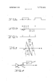
represented by the Secretary of the Attorney-J-larry A. Herbert, Jr. et al. Air Force [22] Filed: July 14, 1972 [57] ABSTRACT [21] Appl. No.: 271,945 A system for deriving synchronizing pulses from a train of digital signals that is fed to in-phase and midphase gates each including an adder with a delay feed- [52] Cl gg g gg g 3 5 back. The output of the mid-phase gate is multiplied I t Cl 5 1/00 HO3k 5/00 by a sign factor determined by a logic circuit connected to the in-phase gate. The output of the two [58] Field of Search 307/208, 269; h d fit d d d 328/63 72 133 178/695 R gates are t en mixe 1 ere an summe M a value dependent upon the' clock rate and fed to a 56 R f C1 d number controlled oscillator which includes a counter 1 e erences and a comparing circuit. The output of the number UNITED STATES PATENTS controlled oscillator is fed back to the in-phase and 3,333,205 7/1967 Featherston 328/63 mid-phase gates. 3,439,279 4/1969 Guanella 328/63 3,510,786 5/1970 Paulson 328/155 2 Claims, 8 Drawing Figures f 11 DETECTED A5 /7 24714 1 D l 9 4 1 .2 6/7? IA/Pur S A; L06
1'5 2 25 I a I 2/ 27 29 3 z; j ,2) F /Z} ""l-15LZv= 1 (mm/7R: e-- 2 F T T T T T T T T T T T T l I v xzssr' I 33 l l dull/T5 2 04 l 700M747! I g N L O I 37 l 39 i l ("35' Nt 1 Q l PATENIEDnuv 13 ms SHEET 2 OF 4 PAIENIEDImY 3 am SHEET 3 CF 4 h ErI F DIGITAL BIT SYNCHRONIZER BACKGROUND OF THE INVENTION SUMMARY OF THE INVENTION The digital bit synchronizer is basically a digital phase lock loop which is capable of tracking samples as a binary waveform. Since transitions may or may not occur between adjacent bits, a nonlinear operation is required in the phase detector to insure the output has the proper sign.
It is an object of this invention to provide a novel and improved system for synchronizing bits from a train of digital samples.
It is another object to provide a synchronizer in the form of a digital phase-locked loop which is capable of tracking samples of a binary data waveform.
It is yet another object to provide a system for synchronizing bits of a binary waveform where transitions may occur between adjacent bits.
These and other objects, features and advantages of the invention will become more apparent from the following description taken in connection with the illustrative embodiments in the accompanying drawings.
DESCRIPTION OF THE DRAWINGS FIGS. 1a through 1c are waveform diagrams showing the derivation of bit synchronizing pulses derived from a data impulse wave.
FIG. 2 is an input/output detector characteristic curve of the digital bit synchronizer.
FIG. 3 is a block diagram showing an embodiment of the invention;
FIG. 4 is a block diagram of the loop filter used in the embodiment of FIG. 3;
FIG. 5 is a block diagram showing the details of the in-phase and mid-phase detectors and associated logic used in the embodiment of FIG. 3; and
FIG. 6 is a block diagram of the number controlled oscillator used in the embodiment of FIG. 3.
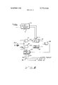
DETAILED DESCRIPTION OF THE PREFERRED EMBODIMENTS Digital data detectors generally require some type of bit synchronization usually derived from the received signals. The present invention has the capability of deriving bits from a sequence of digital samples taken from a binary waveform such as that shown in FIG. la which is a basic data waveform having a pulsewidth of T. Samples are taken as shown in FIG. lb, the samples being represented by arrows with the time difference between samples being shown'as T,. The bit synchronization pulses are then derived and are shown in FIG. 10
as vertical lines.
In order to illustrate a means of obtaining a measure of the phase error, consider the set of samples 8,, S S; from one bit and S S S from the previous bit where S is the most recent sample.
A means of generating the phase error signal is as follows. The phase error signal is generated by a midphase (MP) gate which performs the summation,
12 8MP: 2 SI an in-phase (IP) gate forms the sums and 16 shut-1 5,
The output of the mid-phase gate is then multiplied by +1, 0, or 1, based on the following logic rules:
S, (nl) O, S, (n) 0;-multiply by +1 (opposite signs) S, (nl) 0, S, (n) 0; multiply by -l (opposite signs) S, (nl) and S, (n) are the same sign; multiply by 0.
The resulting phase error detector characteristic is shown in FIG. 2 where A represents the signal amplitude, N the number of samples in the mid-phase gate, 2A the step height, and l/N the step width.
A block diagram of the digital bit synchronizer employing the in-phase and mid-phase (IP/MP) detectors is shown in FIG. 3. The digital input signal is fed to inphase gate 11 together with the clock pulses. Gate 11 includes summing circuit 13 and feedback delay 15. The sign is determined by circuit 17 and then fed to logic circuit 19 where the logic previously explained is performed. The digital input data and clock pulses are also fed to mid-phase gate 21 including summing circuit 23 and feed-back delay 25. The output of midphase gate 21 is fed to delay circuit 27 and is then mixed in mixer 29 with the output of logic circuit 19. The output of mixer 29 is a phase error signal and is smoothed in loop filter 31. This filter is shown as FIG. 4 and includes amplifier 41 fed by the phase error signal and summer 43 having feedback loop 45. The output of filter 41 designated as N is fed to summing circuit 33 which is also fed by a value equal to N, T/T where T time length of the sample and T pulse period of the clock. The N value is such that the digital bit synchronizer operates at the data rate where there is no error number present. The N signal shrinks the gate size until the phase lock is achieved, i.e., the phase error is zero. The output of summer 33 is fed to number control oscillator (NCO) 35 which includes comparing circuit 39 and counter 37. This circuit is a divide-by-N circuit where N is a variable and programmable. Midphase gate timing is obtained by generating a pulse when the counter reaches half of its total count.
In practice, it may be desired to have the NCO to count a considerably higher rate than the sampling rate to achieve smaller increments between NCO frequenfrom summer 33 after division by divide-by-2 circuit 49. Comparing circuit 47 then controls in-phase gate 11 while comparing circuit 39 controls mid-phase gate 25. a
As an example of the rate of operation, the bit synchronizer was designed and built for operation at a data rate of 19.2 kbps with 20 samples per bit, each sample quantized to a maximum of bits. The synchronizer counts a basic frequency of 300 times the bit rate (5.76 MHz) thus allowing the small changes in phase required for narrow noise bandwidths. The mid-phasegate is eight samples wide (out of 20). The loop filter is a constant gain which results in a first order loop.
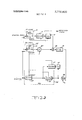
lP/MP gates and associated logic circuits are shown in FIG. 5 as parallel digital accumulators. The inputs to these gates consist of five bits samples coded in twos complement by register 51. The IP accumulator or adder 53 carries nine bits and is fed back through registers 55 and 57. The data output is the sign bit at the end of the integration period through flip-flop 59. midphase gate 21 uses eight bit adder 61 and is fed back through registers 63 and 65. It is dumped after the 16th sample and the output is stored after eight samples have been summed and stored in register 67. Multiplication by 1 consists of inverting the output and adding 1. This is done with inverting gates 69 and 71 through flip- flops 59 and 73 having complementary inputs and outputs and multiplying circuits 75 and 77.
The number controlled oscillator shown in FIG. 6 consists of fixed counters 79 and 81 and variable counter 83. Counter 81, a modulo l5 counter, counts pulses at a rate of 300/T pps. It receives clock pulses through amplifier 85 and gate 87. On the fifteenth count, counter 79, a modulo 20 counter, through gate 89 is advanced by one count. When counter 79 reaches the fifth state the clock line is switched via gate 91 to counter 83 which counts to N,,, the error number out of the loop filter. This addition takes place in error adder 93. The clock line is switched back to counter 81. Lines 95, 96 and 97 are intermediate states of counter 79 used to control the in-phase and mid-phase gates.
The digital bit synchronizer can be built using standard TTL integrated circuits and other available hardware.
What is claimed is:
1. A system for deriving synchronizing pulses from a train of digital signals comprising:
a. a clock;
b. an in-phase gate the timing thereof being controlled by the clock including 1. a first adder fed by the train of digital signals,
and
2. a first register connecting the output of the first adder to the input in a feedback loop;
c. a multiplying logic circuit fed by the in-phase gate, the multiplying factor being dependent upon the sum within the in-phase gate;
d. a mid-phase gate the timing thereof being controlled by the clock including a l. a second adder fed by the train of digital signals,
and 2. a second register connecting the output of the second adder to the input in a feedback loop;
e. a mixer fed by the logic circuit and the mid-phase gate;
f. a filter fed by the mixer;
g. a summing circuit fed by the filter and a signal the value thereof being equal to the ratio of the time length of a digital signal to the pulse period of the clock;
h. a counter fed by the clock;
i. a first comparing circuit fed by the counter and the summing circuit, the output of the first comparing circuit being fed to the counter as a reset pulse; and
j. a second comparing circuit fed by the counter and the summing circuit, the output of the second comparing circuit being fed to the multiplying logic circuit.
2. A system for deriving synchronizing pulses according to claim 1 wherein the multiplying logic circuit includes:
a. a first flip-flop having complementary inputs and outputs, the inputs being fed by the in-phase gate;
b. a second flip-flop fed by the complementary outputs of the first flip-flop;
c. a first inverting gate fed by one output of each of the first and second flip-flops; and
d. a second inverting gate fed by the opposite outputs of the first and second flip-flops from that fed to the first inverting gate.
Claims (4)
1. A system for deriving synchronizing pulses from a train of digital signals comprising: a. a clock; b. an in-phase gate the timing thereof being controlled by the clock including 1. a first adder fed by the train of digital signals, and 2. a first register connecting the output of the first adder to the input in a feedback loop; c. a multiplying logic circuit fed by the in-phase gate, the multiplying factor being dependent upon the sum within the inphase gate; d. a mid-phase gate the timing thereof being controlled by the clock including 1. a second adder fed by the train of digital signals, and 2. a second register connecting the output of the second adder to the input in a feedback loop; e. a mixer fed by the logic circuit and the mid-phase gate; f. a filter fed by the mixer; g. a summing circuit fed by the filter and a signal the value thereof being equal to the ratio of the time length of a digital signal to the pulse period of the clock; h. a counter fed by the clock; i. a first comparing circuit fed by the counter and the summing circuit, the output of the first comparing circuit being fed to the counter as a reset pulse; and j. a second comparing circuit fed by the counter and the summing circuit, the output of the second comparing circuit being fed to the multiplying logic circuit.
2. a first register connecting the output of the first adder to the input in a feedback loop; c. a multiplying logic circuit fed by the in-phase gate, the multiplying factor being dependent upon the sum within the in-phase gate; d. a mid-phase gate the timing thereof being controlled by the clock including
2. a second register connecting the output of the second adder to the input in a feedback loop; e. a mixer fed by the logic circuit and the mid-phase gate; f. a filter fed by the mixer; g. a summing circuit fed by the filter and a signal the value thereof being equal to the ratio of the time length of a digital signal to the pulse period of the clock; h. a counter fed by the clock; i. a first comparing circuit fed by the counter and the summing circuit, the output of the first comparing circuit being fed to the counter as a reset pulse; and j. a second comparing circuit fed by the counter and the summing circuit, the output of the second comparing circuit being fed to the multiplying logic circuit.
2. A system for deriving synchronizing pulses according to claim 1 wherein the multiplying logic circuit includes: a. a first flip-flop having complementary inputs and outputs, the inputs being fed by the in-phase gate; b. a second flip-flop fed by the complementary outputs of the first flip-flop; c. a first inverting gate fed by one output Of each of the first and second flip-flops; and d. a second inverting gate fed by the opposite outputs of the first and second flip-flops from that fed to the first inverting gate.
Applications Claiming Priority (1)
| Application Number | Priority Date | Filing Date | Title |
|---|---|---|---|
| US27194572A | 1972-07-14 | 1972-07-14 |
Publications (1)
| Publication Number | Publication Date |
|---|---|
| US3772600A true US3772600A (en) | 1973-11-13 |
Family
ID=23037759
Family Applications (1)
| Application Number | Title | Priority Date | Filing Date |
|---|---|---|---|
| US00271945A Expired - Lifetime US3772600A (en) | 1972-07-14 | 1972-07-14 | Digital bit synchronizer |
Country Status (1)
| Country | Link |
|---|---|
| US (1) | US3772600A (en) |
Cited By (8)
| Publication number | Priority date | Publication date | Assignee | Title |
|---|---|---|---|---|
| US3928726A (en) * | 1974-11-22 | 1975-12-23 | Bell Telephone Labor Inc | Common control variable shift reframe circuit |
| US3944858A (en) * | 1973-11-22 | 1976-03-16 | Telefonaktiebolaget L M Ericsson | Arrangement for generating pulse sequences |
| US4020283A (en) * | 1975-11-04 | 1977-04-26 | International Telephone And Telegraph Corporation | MSK digital data synchronization detector |
| US4028490A (en) * | 1975-11-14 | 1977-06-07 | International Telephone And Telegraph Corporation | MSK digital data synchronization detector |
| US4043438A (en) * | 1976-04-27 | 1977-08-23 | Litton Business Systems, Inc. | Printing control circuit |
| US4280224A (en) * | 1979-06-21 | 1981-07-21 | Ford Aerospace & Communications Corporation | Bit synchronizer with early and late gating |
| FR2588088A1 (en) * | 1985-10-02 | 1987-04-03 | Ando Electric | DEVICE FOR GENERATING TIME SIGNALS |
| US5602883A (en) * | 1993-10-13 | 1997-02-11 | The United States Of America As Represented By The Administrator Of The National Aeronautics And Space Administration | Method of implementing digital phase-locked loops |
Citations (6)
| Publication number | Priority date | Publication date | Assignee | Title |
|---|---|---|---|---|
| US3333205A (en) * | 1964-10-02 | 1967-07-25 | Ibm | Timing signal generator with frequency keyed to input |
| US3439279A (en) * | 1965-11-26 | 1969-04-15 | Patelhold Patentverwertung | Synchronizing system for random sequence pulse generators |
| US3510786A (en) * | 1967-07-17 | 1970-05-05 | Ibm | Synchronizing circuit compensating for data bit shift |
| US3544907A (en) * | 1966-06-08 | 1970-12-01 | Hasler Ag | Apparatus for generating synchronised timing pulses in a receiver of binary data signals |
| US3566155A (en) * | 1968-06-25 | 1971-02-23 | Itt | Bit synchronization system |
| US3646452A (en) * | 1971-02-16 | 1972-02-29 | Ibm | Second order digital phaselock loop |
-
1972
- 1972-07-14 US US00271945A patent/US3772600A/en not_active Expired - Lifetime
Patent Citations (6)
| Publication number | Priority date | Publication date | Assignee | Title |
|---|---|---|---|---|
| US3333205A (en) * | 1964-10-02 | 1967-07-25 | Ibm | Timing signal generator with frequency keyed to input |
| US3439279A (en) * | 1965-11-26 | 1969-04-15 | Patelhold Patentverwertung | Synchronizing system for random sequence pulse generators |
| US3544907A (en) * | 1966-06-08 | 1970-12-01 | Hasler Ag | Apparatus for generating synchronised timing pulses in a receiver of binary data signals |
| US3510786A (en) * | 1967-07-17 | 1970-05-05 | Ibm | Synchronizing circuit compensating for data bit shift |
| US3566155A (en) * | 1968-06-25 | 1971-02-23 | Itt | Bit synchronization system |
| US3646452A (en) * | 1971-02-16 | 1972-02-29 | Ibm | Second order digital phaselock loop |
Cited By (8)
| Publication number | Priority date | Publication date | Assignee | Title |
|---|---|---|---|---|
| US3944858A (en) * | 1973-11-22 | 1976-03-16 | Telefonaktiebolaget L M Ericsson | Arrangement for generating pulse sequences |
| US3928726A (en) * | 1974-11-22 | 1975-12-23 | Bell Telephone Labor Inc | Common control variable shift reframe circuit |
| US4020283A (en) * | 1975-11-04 | 1977-04-26 | International Telephone And Telegraph Corporation | MSK digital data synchronization detector |
| US4028490A (en) * | 1975-11-14 | 1977-06-07 | International Telephone And Telegraph Corporation | MSK digital data synchronization detector |
| US4043438A (en) * | 1976-04-27 | 1977-08-23 | Litton Business Systems, Inc. | Printing control circuit |
| US4280224A (en) * | 1979-06-21 | 1981-07-21 | Ford Aerospace & Communications Corporation | Bit synchronizer with early and late gating |
| FR2588088A1 (en) * | 1985-10-02 | 1987-04-03 | Ando Electric | DEVICE FOR GENERATING TIME SIGNALS |
| US5602883A (en) * | 1993-10-13 | 1997-02-11 | The United States Of America As Represented By The Administrator Of The National Aeronautics And Space Administration | Method of implementing digital phase-locked loops |
Similar Documents
| Publication | Publication Date | Title |
|---|---|---|
| US4030045A (en) | Digital double differential phase-locked loop | |
| US3464018A (en) | Digitally controlled frequency synthesizer | |
| GB1143758A (en) | ||
| US4242639A (en) | Digital phase lock circuit | |
| EP0373768B1 (en) | Digital frequency divider | |
| GB1436933A (en) | Phase and/or frequency comparators | |
| US5418822A (en) | Configuration for clock recovery | |
| US3772600A (en) | Digital bit synchronizer | |
| US3764903A (en) | Phase measuring system | |
| JPS61237542A (en) | Digital signal detector | |
| US3758720A (en) | Circuit for incrementally phasing digital signals | |
| US3430143A (en) | Communications system wherein information is represented by the phase difference between adjacent tones | |
| US4059806A (en) | Pulse position demodulator circuit | |
| US3490049A (en) | Demodulation of digital information signals of the type using angle modulation of a carrier wave | |
| US5920211A (en) | Fully digital clock synthesizer | |
| EP0237753A1 (en) | A frequency multiplier circuit | |
| US2514671A (en) | Decoder for pulse code modulation | |
| GB987732A (en) | Variable frequency oscillator | |
| US3059188A (en) | Apparatus and method for linear synchronous detection of digital data signals | |
| US3078451A (en) | Digital time modulator | |
| US3671872A (en) | High frequency multiple phase signal generator | |
| US4777447A (en) | Method and apparatus for a digital difference frequency mixer | |
| US3482171A (en) | Bidirectional electronic phase shifter | |
| US4464769A (en) | Method and apparatus for synchronizing a binary data signal | |
| US3651416A (en) | Digital parallax discriminator system |