US3760107A - Time division multiplex communication systems - Google Patents
Time division multiplex communication systems Download PDFInfo
- Publication number
- US3760107A US3760107A US00126527A US12652771A US3760107A US 3760107 A US3760107 A US 3760107A US 00126527 A US00126527 A US 00126527A US 12652771 A US12652771 A US 12652771A US 3760107 A US3760107 A US 3760107A
- Authority
- US
- United States
- Prior art keywords
- initial connection
- test
- switching stage
- gate
- control means
- Prior art date
- Legal status (The legal status is an assumption and is not a legal conclusion. Google has not performed a legal analysis and makes no representation as to the accuracy of the status listed.)
- Expired - Lifetime
Links
Images

Classifications
-
- H—ELECTRICITY
- H04—ELECTRIC COMMUNICATION TECHNIQUE
- H04Q—SELECTING
- H04Q11/00—Selecting arrangements for multiplex systems
- H04Q11/02—Selecting arrangements for multiplex systems for frequency-division multiplexing
-
- H—ELECTRICITY
- H04—ELECTRIC COMMUNICATION TECHNIQUE
- H04J—MULTIPLEX COMMUNICATION
- H04J3/00—Time-division multiplex systems
- H04J3/02—Details
- H04J3/14—Monitoring arrangements
-
- H—ELECTRICITY
- H04—ELECTRIC COMMUNICATION TECHNIQUE
- H04Q—SELECTING
- H04Q11/00—Selecting arrangements for multiplex systems
- H04Q11/04—Selecting arrangements for multiplex systems for time-division multiplexing
Definitions
- ABSTRACT A time division multiplex telephone system has testing apparatus for testing the setting-up of a communication path between two subscribers before the path is switched through to the subscribers. Circuits responsive to signals emitted by the testing apparatus initiate a further attempt to set up the communication path if the testing apparatus signals that the test made on the set up connection indicate that the setting up is not successful.
- This invention relates to time division multiplex (TDM) telecommunication systems especially those in which pulse code modulation is used, and in particular to automatic TDM telephone exchange systems as described in co-pending Patent Application No. 782,541 by the present Applicants and others (now U.S. Pat. No. 3,622,705 issued Nov. 23, 1971) and the content of which is incorporated herein by reference and constitutes the setting to which the present invention relates.
- TDM time division multiplex
- registers are employed to receive and store input information and control the attempt of setting up a connection through the system. After a successful set-up is completed or if this is not possible, a signal, e.g. busy tone, is returned, and the controlling register is released.
- a signal e.g. busy tone
- a time division multiplex communication system comprises test initiating means for confinning a successful attempt to set-up of a connection, and means for initiating a further attempt to set up the connection if the test initiating means do not confirm a successful first attempt.
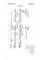
- FIG. I shows in logical form the circuit in the register
- FIG. 2 shows in logical form a connection path through the exchange system.
- the diagram represents NAND gates to positive logic and its operation will be described in terms of voltage levels of two binary states which are used to represent the and 1 conditions of binary logic.
- the state that results in the more positive output volt age is referred to as HIGH and represented by logical l, and that which results in the more negative output voltage as LOW and represented by logical 0.
- Leads on the diagram are labelled in accordance with this nomenclature.
- a lead labelled SET-UP SUCCESSFUL indicates that the named signal occurs when the condition of the lead is in the LOW or logical 0 state, no signal is given whereas the absence of the bar drawn over the designation of the lead would indicate that the named signal occurs when the condition of the lead is HIGH or in the logical 1 state.
- the register operates on a TDM basis for the reception and storing of received information relating to a call, and therefore more than one call can be in this state in a REGISTER at the same time. Only one connection can be set-up at a time and for this reason, each REGISTER is scanned periodically, for example for 3.5 ms every 98 ms, during which time it can attempt to set-up a particular connection.
- Each REGISTER is scanned in turn for a period of RSn (e.g. 3.5 ms) and 28 values of n are available.
- a REGISTER scan period i.e. say RS 1, comprises 7 multiframes giving 28 frames synchronised with frames F1-4, these 28 frames being designated identified by waveforms E l-28. Details of the generation of the waveforms are to be found in column 4 of U.S. Pat. No. 3,622,705.
- A, B and C switches are employed of which the A switch is written at time E10, the, B switch is written at time E9 and the C switch is written at time E15 or E17. Details of the manner in which the switches are written appears in columns 15 and 16 of U.S. Pat. No. 3,622,705.
- connection is set-up during the REGISTER scan period according to a fixed program controlled'by the 28 waveforms El-28. Complete details of the set-up procedure are to be found in U.S. Pat. No. 3,622,705 commencing at the foot of column 4.
- FIGS. 1 and 2 are, respectively, simpler versions of FIGS. 8a, 8b, 8e and 8f combined together and FIGS. 30, 3d, 5a, 5b, 6a, 6b, 14 and 15a combined together of U.S. Pat. No. 3,622,705.
- the setting up sequence is briefly that the REGIS- TER sends a forward marking signal to INDICATE the calling channel and a backward marking signal to MARK the route required. Checks are made to ensure (a) that no signals are received from the exchange before the connection is set-up and (b) that the CIRCUIT FREE signal is received after the set-up is completed. The marking signals are then removed, a test signal is sent to the terminating end, and a further check is made to see that the CIRCUIT FREE signal is removed. If it is, the REGISTER releases.
- REGISTER SEND EXCHANGE HOLD A channel is selected before the start of the REGIS- TER scan period, and the REGISTER immediately starts to send an EXCHANGE HOLD signal on the REG.SEND.(EXCHANGE) (FIG. 2) lead in all EVEN frames.
- the signals are delayed by one-half digit, i.e.
- T C A LOW output at TD 8/l .TC.SC.(F2 F4) sets the latched gate pair RD 33-34, which is reset by TC. This signal is sent during the whole time a channel is selected, except for the period [32-8 of RSn, when it is inhibited in order to release a B-SWITCH which may be held from a first attempt, and constitutes the hold signal for the initial attempt to set-up the connection.
- the forward INDICATE signal is sent out in the selected channel at the start of RSn and is repeated every frame until the CIRCUIT FREE signal is received back from the exchange indicating that the set-up has been completed.
- the INDICATE signal is a HIGH signal delayed by one-half digit and stretched to the beginning of TD 8/6. Further details of the procedure just described are to be found in column 10 of U.S. Pat. No. 3,622,705.
- the CIRCUIT AVAILABLE latched gate pair RD28-29 will be reset and the output of gate RD29 will be HIGH.
- the INDICATE signal is then generated by setting the latched gate pair RD37- 38 at TCTD 8/1 via gate RD36, resetting it at TD 8/6, and gating the output with RSn.SC in gate RD39.
- REGISTER CHECKS made are, in detail, as follows:
- D] should be LOW(O) in both ODD and EVEN frames.
- gate RDS output of gate RDS is sampled at E13 and E15 of RSn via gates RD8 and RD9, and if the latched-gate pair RD5-6 is set, the SECOND ATTEMPT latched-gate pair RD15-16 is set via gate RD7.
- the REGISTER writes the C SWITCH in E15 or E17 of RSn over the REG.
- CIR- CUIT FREE signal i.e. D1 HIGH (1) in ODD frames, should be received from the terminating end of the outgoing PCM system. If this is received, the latched-gate pair RD5-6 should be set and the SECOND ATTEMPT latched-gate pair RD15-16 will not be set. Further details of this operation appear in column 16 of U.S. Pat. No. 3,622,705.
- latched-gate pair RD5-6 will not be set and the output of gate RD6 is sampled at E19 and E21 of RSn in gate RDlO via gate RDll, and latched-gate pair RD15-16 will be set.
- the CIRCUIT AVAILABLE latched-gate pair RD28-29 has already been set and the output of gate RD28 is HIGH. Under these conditions latched-gate pair RD53-54 is set via gate RD52.
- gate RD53 is gated with the selected channel in gate RD55 to provide the output signal SET- UP SUCCESSFUL.
- the second attempt is made in the next RSn period following the first attempt, and the set-up procedure is exactly as described for that attempt. If one of the REGISTER checks is faulty the second attempt latched-gate pair RDl5-16 is again set, but now that the latched-gate pair RDl8-l9 is set a LOW output is obtained from gate RD at SC.El6.RS(n+3) indicating that the second attempt is unsuccessful. This output causes the N.U. tone STORE to be written and this will result in the removal of the EXCHANGE HOLD signal from the REG. REC. (LINE).
- the latched gate pair RD 18-19 is reset from gate RD2I via gate RD22 when the REGISTER HOLD disappears, and from the output of gate RD55 if the second attempt is successful.
- REGISTER RELEASE If the set-up is unsatisfactory for any reason a signal is sent from the REGISTER to write the N.U. tone STORE. This is a HIGH signal in D1.F2 on the REG. SEND (LINE). As is described in the Specification referred to above, all those REGISTER fault indications that occur at channel time are included in three of the inputs to gate RD81 and the fourth input is from gate RA64. The HIGH output from gate RD81 in the event of a fault is gated with the SHORT HOLD at gate RD82 and used to write the REGISTER RELEASE STORE.
- a CALLS LOST output is provided from gate RD82 to the TRAFFIC RECORDER.
- REGISTER RELEASE STORE The output of the REGISTER RELEASE STORE is gated with R2 at gate RD60 and applied to gate RD61, from which it is sent to REG. SEND. (LINE) lead.
- REG. SEND. (LINE) lead An explanation of the foregoing is to be found in column 12 of U.S. Pat. No. 3,622,705.
- a PATH READER interrogates the common point of the INDICATE paths in the U0 TRUNK UNIT. If a channel pulse is returned, it implies an unsuccessful attempt.
- the returned channel and the identity of the i/c TRUNK UNIT is passed to a PRINT STATICISER and a signal is produced to interrogate the B SWITCHES and the 0/ TRUNK UNITS during E24.
- the identity of the selected B SWITCH, selected CORD, and marked olg TRUNK UNITS is returned and passed to the PRINT STATICISER.
- the identity of the REGISTER is deduced from the REG. SCAN PE- RIOD in which this occurs so that the identity of the REGISTER can also be staticised.
- a failure to set up thus results in a message being printed out giving the REGISTER, calling channel, i/c TRUNK UNIT, B SWITCH, CORD and wanted 0/g ROUTE.
- the PATH READ OUT is dealt with in column 20 of U.S. No. 3,622,705.
- a time division multiplex communication system comprising in combination:
- control means for locating through each of said switching stages a path suitable for the required connections
- control means including test initiating means for A. making a test of the condition of said set-up initial connection
- control means including further means responsive to the failure of either of said tests for attempting to set-up another initial connection.
Landscapes
- Engineering & Computer Science (AREA)
- Computer Networks & Wireless Communication (AREA)
- Signal Processing (AREA)
- Monitoring And Testing Of Exchanges (AREA)
- Use Of Switch Circuits For Exchanges And Methods Of Control Of Multiplex Exchanges (AREA)
- Time-Division Multiplex Systems (AREA)
Abstract
A time division multiplex telephone system has testing apparatus for testing the setting-up of a communication path between two subscribers before the path is switched through to the subscribers. Circuits responsive to signals emitted by the testing apparatus initiate a further attempt to set up the communication path if the testing apparatus signals that the test made on the set up connection indicate that the setting up is not successful.
Description
United States Patent Duerdoth a a1.
[451 Sept. 18,1973
TIME DIVISION MULTIPLEX COMMUNICATION SYSTEMS Inventors: Winston Theodore Duerdoth,
Ruislip; Charles Joseph Hughes, London; John Frederick Hesketh, Greenford; William Desmond Morton, Rickmansworth, all of England Assignee: Her Majestys Postmaster General,
London, England Filed: Mar. 22, 1971 Appl. No.: 126,527
Related US. Application Data Division of Ser. No. 782,541, Dec. 12, 1968.
Foreign Application Priority Data Dec. 11, 1967 Great Britain 56,149/67 [56] References Cited UNITED STATES PATENTS 3,551,601 12/1970 Sloan 179/18 E 3,423,539 1/1969 Page 179/18 E OTHER PUBLICATIONS Bell System Technical Journal; Vol. XLIII, No. 5, Parts 1 and 2; September 1964, pp. 2249-2253 & pp. 1984-1985.
Primary Examiner-Kathleen H. Claffy Assistant Examiner-David L. Stewart Attorney-Hall & I-Ioughton [5 7] ABSTRACT A time division multiplex telephone system has testing apparatus for testing the setting-up of a communication path between two subscribers before the path is switched through to the subscribers. Circuits responsive to signals emitted by the testing apparatus initiate a further attempt to set up the communication path if the testing apparatus signals that the test made on the set up connection indicate that the setting up is not successful.
7 2 Claims, 2 Drawing Figures TH7/n-f-4 RSn+3 E73 E75 R026 70 TRAFFIC R08 R09 rH4n Rt'CORDE/I R03 R07 E79 REG. REC. xc//. 1 R05 R077 R078 R020 PAW zwrrfwr R04 FAILED roe/5 R06 R079 -U/ SUCCESSfl/L 50 R072 R013 1 RSn R E G S T E R TUB/6 R032 REG SEND EXCH.
TIME DIVISION MULTIPLEX COMMUNICATION SYSTEMS This is a division of Application Ser. No. 782,541 filed Dec. 12, 1968.
BACKGROUND OF THE INVENTION This invention relates to time division multiplex (TDM) telecommunication systems especially those in which pulse code modulation is used, and in particular to automatic TDM telephone exchange systems as described in co-pending Patent Application No. 782,541 by the present Applicants and others (now U.S. Pat. No. 3,622,705 issued Nov. 23, 1971) and the content of which is incorporated herein by reference and constitutes the setting to which the present invention relates.
In such systems, registers are employed to receive and store input information and control the attempt of setting up a connection through the system. After a successful set-up is completed or if this is not possible, a signal, e.g. busy tone, is returned, and the controlling register is released.
It is an object of the present invention to provide improved register facilities.
SUMMARY OF INVENTION According to the present invention, a time division multiplex communication system comprises test initiating means for confinning a successful attempt to set-up of a connection, and means for initiating a further attempt to set up the connection if the test initiating means do not confirm a successful first attempt.
Preferably, the system further includes connection hold means for holding the initial setting-up until the further attempt has been made.
In one particular embodiment of the invention, record-providing equipment is included, such equipment providing a record identifying the route over which an unsuccessful initial setting-up was made.
BRIEF DESCRIPTION OF THE DRAWINGS An embodiment of the invention will now be described with reference to the accompanying drawings in which:
FIG. I shows in logical form the circuit in the register, and
FIG. 2 shows in logical form a connection path through the exchange system.
DESCRIPTION OF PREFERRED EMBODIMENTS The time division multiplex communication system of which the embodiment to be described forms a part is that set out in the parent Specification referred to above and to which reference should be made for details of the system itself.
As has been stated in the parent Specification referred to above, the diagram represents NAND gates to positive logic and its operation will be described in terms of voltage levels of two binary states which are used to represent the and 1 conditions of binary logic. The state that results in the more positive output volt age is referred to as HIGH and represented by logical l, and that which results in the more negative output voltage as LOW and represented by logical 0. Leads on the diagram are labelled in accordance with this nomenclature. For example, a lead labelled SET-UP SUCCESSFUL indicates that the named signal occurs when the condition of the lead is in the LOW or logical 0 state, no signal is given whereas the absence of the bar drawn over the designation of the lead would indicate that the named signal occurs when the condition of the lead is HIGH or in the logical 1 state.
The register operates on a TDM basis for the reception and storing of received information relating to a call, and therefore more than one call can be in this state in a REGISTER at the same time. Only one connection can be set-up at a time and for this reason, each REGISTER is scanned periodically, for example for 3.5 ms every 98 ms, during which time it can attempt to set-up a particular connection.
Each REGISTER is scanned in turn for a period of RSn (e.g. 3.5 ms) and 28 values of n are available. A REGISTER scan period, i.e. say RS 1, comprises 7 multiframes giving 28 frames synchronised with frames F1-4, these 28 frames being designated identified by waveforms E l-28. Details of the generation of the waveforms are to be found in column 4 of U.S. Pat. No. 3,622,705.
The Specification referred to above describes the sequence of events leading to the HOLD REGISTER condition. A HOLD signal is obtained and if this persists for more than a predetermined time, 3 sees. in the example being described, the call is to be timed out and number unobtainable tone returned. The REGISTER is also released. Further information regarding the HOLD REGISTER condition occurs in columns 7 and 8 of U.S. Pat. No. 3,622,705.
In the system described in the Specification mentioned above, A, B and C switches are employed of which the A switch is written at time E10, the, B switch is written at time E9 and the C switch is written at time E15 or E17. Details of the manner in which the switches are written appears in columns 15 and 16 of U.S. Pat. No. 3,622,705.
A connection is set-up during the REGISTER scan period according to a fixed program controlled'by the 28 waveforms El-28. Complete details of the set-up procedure are to be found in U.S. Pat. No. 3,622,705 commencing at the foot of column 4.
Of the accompanying drawings, FIGS. 1 and 2 are, respectively, simpler versions of FIGS. 8a, 8b, 8e and 8f combined together and FIGS. 30, 3d, 5a, 5b, 6a, 6b, 14 and 15a combined together of U.S. Pat. No. 3,622,705.
The setting up sequence is briefly that the REGIS- TER sends a forward marking signal to INDICATE the calling channel and a backward marking signal to MARK the route required. Checks are made to ensure (a) that no signals are received from the exchange before the connection is set-up and (b) that the CIRCUIT FREE signal is received after the set-up is completed. The marking signals are then removed, a test signal is sent to the terminating end, and a further check is made to see that the CIRCUIT FREE signal is removed. If it is, the REGISTER releases.
In the event of any of the checks not being satisfactory, a second attempt is made.
REGISTER SEND EXCHANGE HOLD A channel is selected before the start of the REGIS- TER scan period, and the REGISTER immediately starts to send an EXCHANGE HOLD signal on the REG.SEND.(EXCHANGE) (FIG. 2) lead in all EVEN frames. The signals are delayed by one-half digit, i.e.
they are sent out at TD 8/l. T C A LOW output at TD 8/l .TC.SC.(F2 F4) sets the latched gate pair RD 33-34, which is reset by TC. This signal is sent during the whole time a channel is selected, except for the period [32-8 of RSn, when it is inhibited in order to release a B-SWITCH which may be held from a first attempt, and constitutes the hold signal for the initial attempt to set-up the connection.
INDICATE I/C JUNCTION The forward INDICATE signal is sent out in the selected channel at the start of RSn and is repeated every frame until the CIRCUIT FREE signal is received back from the exchange indicating that the set-up has been completed. The INDICATE signal is a HIGH signal delayed by one-half digit and stretched to the beginning of TD 8/6. Further details of the procedure just described are to be found in column 10 of U.S. Pat. No. 3,622,705.
At the start of RSn the CIRCUIT AVAILABLE latched gate pair RD28-29 will be reset and the output of gate RD29 will be HIGH. The INDICATE signal is then generated by setting the latched gate pair RD37- 38 at TCTD 8/1 via gate RD36, resetting it at TD 8/6, and gating the output with RSn.SC in gate RD39.
The signal is inverted before being sent out to the REGISTER CONNECTION SWITCH, and a check is made by gate RD41 to ensure that a permanent INDI- CATE is not being sent out. Further reference to the operation is found in column 10 lines 47-53 of U.S. Pat. No. 3,622,705. 1
The REGISTER CHECKS made are, in detail, as follows:
i. in E 13 and E 15 of RSn, that there are no false signals being received on the REG. REC. EXCH. lead from the C switch through the A and B switches, the crosspoints being operated in both the A and B switches, but not in the C switch. The correct condition on the REG. REC. EXCH. lead under this condition is that D1 should be LOW(O) in both the ODD and EVEN frames, and if so, the C switch is written in either E15 or E17.
ii. that having written the C SWITCH in ETS, that in E 19 and E 21 the CIRCUIT FREE signal is received, i.e. D1 is HIGH(1) in the ODD frames.
iii. after sending a seizure signal in E 25 to the terminating end of the called PCM system, that in E 13 and-E 15 of RS(n+3) the CIRCUIT FREE signal is removed, i.e. D1 should be LOW(O) in both ODD and EVEN frames.
Failure of any of these checks results in a second attempt being made by the REGISTER to set-up the connection as is explained at column 11 of U.S. Pat. No. 3,622,705.
The check circuits to make the checks set out above will now be explained in more detail, the REG. REC. EXCH. lead being gated at gate RD4 by a timing waveform corresponding to TC.TD8/3 generated by gates RBI-3.
i. The correct condition on the REG. REC. EXCH.
' lead is that D] should be LOW(O) in both ODD and EVEN frames.
If any false signals are received they will be HIGH(1) and will result in the latched-gate pair RD5-6 being set and the output from gate RDS stretched to TD 8/6. The
output of gate RDS is sampled at E13 and E15 of RSn via gates RD8 and RD9, and if the latched-gate pair RD5-6 is set, the SECOND ATTEMPT latched-gate pair RD15-16 is set via gate RD7.
ii. the REGISTER writes the C SWITCH in E15 or E17 of RSn over the REG. SEND EXCH. lead and via the A and B SWITCH crosspoints.
With the C SWITCH crosspoints operated, CIR- CUIT FREE signal i.e. D1 HIGH (1) in ODD frames, should be received from the terminating end of the outgoing PCM system. If this is received, the latched-gate pair RD5-6 should be set and the SECOND ATTEMPT latched-gate pair RD15-16 will not be set. Further details of this operation appear in column 16 of U.S. Pat. No. 3,622,705.
If the CIRCUIT FREE signal, i.e. ls in ODD frames, is not received, then latched-gate pair RD5-6 will not be set and the output of gate RD6 is sampled at E19 and E21 of RSn in gate RDlO via gate RDll, and latched-gate pair RD15-16 will be set. Reference should be made to columns 11 and 16 of U.S. Pat, No. 3,622,705 for more detail of the procedure just described.
iii. if the two checks described in (i) and (ii) are satisfactory, i.e. the latched-gate pair RD15-l6 will not have been set, and the circuit available latchedgate pair RD28-29 is set at SC.E22.Rsn via gate RD27, resulting in a seizure signal in TC.TD8/l.SC.Fl being sent via gate RD30 and latched-gate pair RD33-34 on REG. SEND EXCH. lead commencing in E25 of RSn and continuing until the set-up is completed.
This seizure signal received at the terminating end of the outgoing PCM system should result in the CIR- CUIT FREE signal being changed to CIRCUIT BUSY, i.e. D1 LOW(O) in both ODD and EVEN frames. This is checked on REG. REC. EXCH. lead as described in (i), the output of gate RD5 being sampled in E13 and E15, but of RS(n+3) via gates RD8 and RD9.
SET-UP SUCCESSFUL If the REGISTER checks described are successful, the SECOND ATTEMPT latched-gate pair RDl5-16 will not have been set and at E16 of RS(n+3) the output of gate RD16 will be HIGH.
The CIRCUIT AVAILABLE latched-gate pair RD28-29 has already been set and the output of gate RD28 is HIGH. Under these conditions latched-gate pair RD53-54 is set via gate RD52.
The output of gate RD53 is gated with the selected channel in gate RD55 to provide the output signal SET- UP SUCCESSFUL. Reference is made to columns 11 and 12 of U.S. Pat. No. 3,622,705 for further details.
SECOND ATTEMPT If the REGISTER checks described are not successful the second attempt latched gate pair RD15-l6 is set. The checks are completed by El5.RS(n+3) and at E19 the output of the latched-gate pair RD15-16 is sampled at gate RD17 and if a second attempt is required the latched-gate pair RDl8-l9 is set. The output is gated with TH4/n and TH7-/n +4 to provide a single 5 p. s pulse at the beginning of RS(n+4) which provides the SECOND ATTEMPT output for recording purposes.
The second attempt is made in the next RSn period following the first attempt, and the set-up procedure is exactly as described for that attempt. If one of the REGISTER checks is faulty the second attempt latched-gate pair RDl5-16 is again set, but now that the latched-gate pair RDl8-l9 is set a LOW output is obtained from gate RD at SC.El6.RS(n+3) indicating that the second attempt is unsuccessful. This output causes the N.U. tone STORE to be written and this will result in the removal of the EXCHANGE HOLD signal from the REG. REC. (LINE).
The latched gate pair RD 18-19 is reset from gate RD2I via gate RD22 when the REGISTER HOLD disappears, and from the output of gate RD55 if the second attempt is successful.
REGISTER RELEASE If the set-up is unsatisfactory for any reason a signal is sent from the REGISTER to write the N.U. tone STORE. This is a HIGH signal in D1.F2 on the REG. SEND (LINE). As is described in the Specification referred to above, all those REGISTER fault indications that occur at channel time are included in three of the inputs to gate RD81 and the fourth input is from gate RA64. The HIGH output from gate RD81 in the event of a fault is gated with the SHORT HOLD at gate RD82 and used to write the REGISTER RELEASE STORE.
A CALLS LOST output is provided from gate RD82 to the TRAFFIC RECORDER.
The output of the REGISTER RELEASE STORE is gated with R2 at gate RD60 and applied to gate RD61, from which it is sent to REG. SEND. (LINE) lead. An explanation of the foregoing is to be found in column 12 of U.S. Pat. No. 3,622,705.
PATH READ OUT If the set up is unsuccessful it may be desired to print out the details of the unsatisfactory attempt.
During E23 a PATH READER interrogates the common point of the INDICATE paths in the U0 TRUNK UNIT. If a channel pulse is returned, it implies an unsuccessful attempt. The returned channel and the identity of the i/c TRUNK UNIT is passed to a PRINT STATICISER and a signal is produced to interrogate the B SWITCHES and the 0/ TRUNK UNITS during E24. The identity of the selected B SWITCH, selected CORD, and marked olg TRUNK UNITS is returned and passed to the PRINT STATICISER. The identity of the REGISTER is deduced from the REG. SCAN PE- RIOD in which this occurs so that the identity of the REGISTER can also be staticised.
A failure to set up thus results in a message being printed out giving the REGISTER, calling channel, i/c TRUNK UNIT, B SWITCH, CORD and wanted 0/g ROUTE.
The PATH READ OUT is dealt with in column 20 of U.S. No. 3,622,705.
We claim:
1. A time division multiplex communication system comprising in combination:
1. a plurality of communication channels;
2. a number of switching stages including a first switching stage and a last switching stage for providing a required connection between first and second channels of said plurality;
3. control means for locating through each of said switching stages a path suitable for the required connections; and
4. means for setting up, once each said path is located, an. initial connection through said first switching stage as far as but not through said last switching stage;
5. said control means including test initiating means for A. making a test of the condition of said set-up initial connection,
B. effecting an extension of said set-up initial connection through said last switching stage if said test is successful, and further C. making a test of the condition of said extended set-up initial connection to verify whether a signal is receivable by said control means over said exended set-up initial connection, and
6. said control means including further means responsive to the failure of either of said tests for attempting to set-up another initial connection.
2. A system as claimed in claim 1, which further comprises hold means for holding at least a part of said setup initial connection until the attempt to set-up another initial connection has been made.
Claims (7)
1. A time division multiplex communication system comprising in combination: 1. a plurality of communication channels; 2. a number of switching stages including a first switching stage and a last switching stage for providing a required connection between first and second channels of said plurality; 3. control means for locating through each of said switching stages a path suitable for the required connections; and 4. means for setting up, once each said path is located, an initial connection through said first switching stage as far as but not through said last switching stage; 5. said control means including test initiating means for A. making a test of the condition of said set-up initial connection, B. effecting an extension of said set-up initial connection through said last switching stage if said test is successful, and further C. making a test of the condition of said extended set-up initial connection to verify whether a signal is receivable by said control means over said exended set-up initial connection, and 6. said control means including further means responsive to the failure of either of said tests for attempting to set-up another initial connection.
2. a number of switching stages including a first switching stage and a last switching stage for providing a required connection between first and second channels of said plurality;
2. A system as claimed in claim 1, which further comprises hold means for holding at least a part of said set-up initial connection until the attempt to set-up another initial connection has been made.
3. control means for locating through each of said switching stages a path suitable for the required connections; and
4. means for setting up, once each said path is located, an initial connection through said first switching stage as far as but not through said last switching stage;
5. said control means including test initiating means for A. making a test of the condition of said set-up initial connection, B. effecting an extension of said set-up initial connection through said last switching stage if said test is successful, and further C. making a test of the condition of said extended set-up initial connection to verify whether a signal is receivable by said control means over said exended set-up initial connection, and
6. said control means including further means responsive to the failure of either of said tests for attempting to set-up another initial connection.
Applications Claiming Priority (1)
| Application Number | Priority Date | Filing Date | Title |
|---|---|---|---|
| GB5614967 | 1967-12-11 |
Publications (1)
| Publication Number | Publication Date |
|---|---|
| US3760107A true US3760107A (en) | 1973-09-18 |
Family
ID=10475857
Family Applications (4)
| Application Number | Title | Priority Date | Filing Date |
|---|---|---|---|
| US782541A Expired - Lifetime US3622705A (en) | 1967-12-11 | 1968-12-10 | Telecommunication switching systems |
| US00126527A Expired - Lifetime US3760107A (en) | 1967-12-11 | 1971-03-22 | Time division multiplex communication systems |
| US00126518A Expired - Lifetime US3760115A (en) | 1967-12-11 | 1971-03-22 | Crosspoint error detection in time division multiplex switching systems |
| US00126516A Expired - Lifetime US3760114A (en) | 1967-12-11 | 1971-03-22 | Fault discrimination circuit |
Family Applications Before (1)
| Application Number | Title | Priority Date | Filing Date |
|---|---|---|---|
| US782541A Expired - Lifetime US3622705A (en) | 1967-12-11 | 1968-12-10 | Telecommunication switching systems |
Family Applications After (2)
| Application Number | Title | Priority Date | Filing Date |
|---|---|---|---|
| US00126518A Expired - Lifetime US3760115A (en) | 1967-12-11 | 1971-03-22 | Crosspoint error detection in time division multiplex switching systems |
| US00126516A Expired - Lifetime US3760114A (en) | 1967-12-11 | 1971-03-22 | Fault discrimination circuit |
Country Status (10)
| Country | Link |
|---|---|
| US (4) | US3622705A (en) |
| AU (2) | AU6691074A (en) |
| BE (1) | BE725296A (en) |
| CH (1) | CH514964A (en) |
| DE (1) | DE1814067A1 (en) |
| ES (6) | ES361299A1 (en) |
| FR (1) | FR1597786A (en) |
| GB (1) | GB1257623A (en) |
| NL (1) | NL6817772A (en) |
| SE (6) | SE357482B (en) |
Cited By (4)
| Publication number | Priority date | Publication date | Assignee | Title |
|---|---|---|---|---|
| US3909562A (en) * | 1974-09-12 | 1975-09-30 | Int Standard Electric Corp | Switching network testing process and arrangement |
| US3937895A (en) * | 1973-02-22 | 1976-02-10 | Otto Karl | Circuit arrangement for detecting double connections in digital telecommunication switching systems |
| US4398271A (en) * | 1979-12-07 | 1983-08-09 | Institut Francais Du Petrole | Device for data transmission between seismic data acquisition devices and a recording device |
| US4429391A (en) | 1981-05-04 | 1984-01-31 | Bell Telephone Laboratories, Incorporated | Fault and error detection arrangement |
Families Citing this family (8)
| Publication number | Priority date | Publication date | Assignee | Title |
|---|---|---|---|---|
| FR2119152A5 (en) * | 1970-12-22 | 1972-08-04 | Lannionnais Electronique | |
| DE2102371B2 (en) * | 1971-01-19 | 1972-07-13 | Siemens AG, 1000 Berlin u. 8000 München | CIRCUIT ARRANGEMENT FOR MONITORING PCM COUPLING DEVICES |
| GB1504897A (en) * | 1974-08-09 | 1978-03-22 | Ericsson L M Pty Ltd | Method for through connection check in digital data systems |
| DE2529475C3 (en) * | 1975-07-02 | 1981-10-08 | Ewald Max Christian Dipl.-Phys. 6000 Frankfurt Hennig | Electrical circuit arrangement for time-dependent measurement of physical quantities |
| US4371758A (en) * | 1981-06-08 | 1983-02-01 | Bell Telephone Laboratories, Incorporated | Defective short holding-time trunk identifying method |
| GB8923158D0 (en) * | 1989-10-13 | 1989-11-29 | Plessey Telecomm | Fault detection and bandwidth monitoring means for an atd switch |
| JP3895912B2 (en) * | 2000-09-01 | 2007-03-22 | 矢崎総業株式会社 | Control unit and multiplex communication system |
| CN113285852B (en) * | 2021-05-14 | 2022-11-11 | 李国志 | Method for realizing synchronous test of multi-path E1 signals |
Citations (2)
| Publication number | Priority date | Publication date | Assignee | Title |
|---|---|---|---|---|
| US3423539A (en) * | 1964-11-09 | 1969-01-21 | Gen Electric Co Ltd | Automatic telephone exchange switching systems |
| US3551601A (en) * | 1968-04-02 | 1970-12-29 | American Telephone & Telegraph | Equipment for automatically retrying customer dialed calls |
Family Cites Families (22)
| Publication number | Priority date | Publication date | Assignee | Title |
|---|---|---|---|---|
| US2878327A (en) * | 1956-11-06 | 1959-03-17 | Sperry Rand Corp | High gain magnetic amplifier |
| US3047840A (en) * | 1960-02-03 | 1962-07-31 | Harms Victor | Translators for multi-channel codes employing matrices |
| US3217106A (en) * | 1960-03-14 | 1965-11-09 | Nippon Electric Co | Time-slot interchange circuit |
| DE1206970B (en) * | 1960-05-09 | 1965-12-16 | Fuji Tsushinki Seizo Kabushiki | Circuit arrangement for the time shifting of message channels in time division multiplex message systems |
| US3263030A (en) * | 1961-09-26 | 1966-07-26 | Rca Corp | Digital crosspoint switch |
| NL273091A (en) * | 1961-12-29 | |||
| US3160852A (en) * | 1962-03-19 | 1964-12-08 | Bell Telephone Labor Inc | Checking circuit |
| BE637591A (en) * | 1962-09-19 | |||
| NL299267A (en) * | 1963-04-15 | |||
| DE1278544B (en) * | 1963-09-23 | 1968-09-26 | Siemens Ag | Method and circuit arrangement for transmitting several pulse-modulated telecommunications messages over a common transmission path in time division multiplex systems, in particular time division multiplex telephone exchanges |
| US3337849A (en) * | 1963-11-26 | 1967-08-22 | Bell Telephone Labor Inc | Matrix control having both signal and crosspoint fault detection |
| FR1443867A (en) * | 1963-12-24 | 1966-07-01 | Signaling emission control system | |
| US3348198A (en) * | 1964-08-04 | 1967-10-17 | Bell Telephone Labor Inc | Code-checking comparator circuit |
| US3371315A (en) * | 1964-08-05 | 1968-02-27 | Bell Telephone Labor Inc | Error detection circuit for translation system |
| US3376393A (en) * | 1964-09-22 | 1968-04-02 | North Electric Co | Method of and apparatus for providing different release signals with detection of search busy or cut-through busy condition in a saturation signalling system |
| FR1439029A (en) * | 1964-12-24 | 1966-05-20 | Constr Telephoniques | Improvements to switchgear monitoring systems |
| US3340363A (en) * | 1965-01-26 | 1967-09-05 | Stromberg Carlson Corp | Signal amplitude sequenced time division multiplex communication system |
| US3461242A (en) * | 1965-02-24 | 1969-08-12 | Bell Telephone Labor Inc | Time division switching system |
| US3458659A (en) * | 1965-09-15 | 1969-07-29 | New North Electric Co | Nonblocking pulse code modulation system having storage and gating means with common control |
| US3449526A (en) * | 1966-04-08 | 1969-06-10 | Itt | Trap circuit for use in an electronic switching telephone system |
| US3588367A (en) * | 1968-08-07 | 1971-06-28 | Itt | Monitor and alarm circuit for self-seeking network |
| US3586784A (en) * | 1969-04-10 | 1971-06-22 | Itt | Cross-point-switching arrangement |
-
1967
- 1967-12-11 GB GB5614967A patent/GB1257623A/en not_active Expired
-
1968
- 1968-12-10 US US782541A patent/US3622705A/en not_active Expired - Lifetime
- 1968-12-11 BE BE725296D patent/BE725296A/xx unknown
- 1968-12-11 CH CH1847368A patent/CH514964A/en not_active IP Right Cessation
- 1968-12-11 SE SE16945/68A patent/SE357482B/xx unknown
- 1968-12-11 FR FR1597786D patent/FR1597786A/fr not_active Expired
- 1968-12-11 ES ES361299A patent/ES361299A1/en not_active Expired
- 1968-12-11 SE SE7115344A patent/SE372394B/xx unknown
- 1968-12-11 SE SE7115343A patent/SE373254B/xx unknown
- 1968-12-11 DE DE19681814067 patent/DE1814067A1/en active Pending
- 1968-12-11 NL NL6817772A patent/NL6817772A/xx unknown
-
1970
- 1970-08-14 ES ES382769A patent/ES382769A1/en not_active Expired
- 1970-08-14 ES ES382772A patent/ES382772A1/en not_active Expired
- 1970-08-14 ES ES382771A patent/ES382771A1/en not_active Expired
- 1970-08-14 ES ES382770A patent/ES382770A1/en not_active Expired
- 1970-08-14 ES ES382768A patent/ES382768A1/en not_active Expired
-
1971
- 1971-03-22 US US00126527A patent/US3760107A/en not_active Expired - Lifetime
- 1971-03-22 US US00126518A patent/US3760115A/en not_active Expired - Lifetime
- 1971-03-22 US US00126516A patent/US3760114A/en not_active Expired - Lifetime
- 1971-11-30 SE SE7115342A patent/SE7115342L/sv unknown
- 1971-11-30 SE SE7115341A patent/SE7115341L/sv unknown
- 1971-11-30 SE SE7115345A patent/SE7115345L/sv unknown
-
1974
- 1974-03-21 AU AU66910/74A patent/AU6691074A/en not_active Expired
- 1974-03-21 AU AU66913/74A patent/AU6691374A/en not_active Expired
Patent Citations (2)
| Publication number | Priority date | Publication date | Assignee | Title |
|---|---|---|---|---|
| US3423539A (en) * | 1964-11-09 | 1969-01-21 | Gen Electric Co Ltd | Automatic telephone exchange switching systems |
| US3551601A (en) * | 1968-04-02 | 1970-12-29 | American Telephone & Telegraph | Equipment for automatically retrying customer dialed calls |
Non-Patent Citations (1)
| Title |
|---|
| Bell System Technical Journal; Vol. XLIII, No. 5, Parts 1 and 2; September 1964, pp. 2249 2253 & pp. 1984 1985. * |
Cited By (4)
| Publication number | Priority date | Publication date | Assignee | Title |
|---|---|---|---|---|
| US3937895A (en) * | 1973-02-22 | 1976-02-10 | Otto Karl | Circuit arrangement for detecting double connections in digital telecommunication switching systems |
| US3909562A (en) * | 1974-09-12 | 1975-09-30 | Int Standard Electric Corp | Switching network testing process and arrangement |
| US4398271A (en) * | 1979-12-07 | 1983-08-09 | Institut Francais Du Petrole | Device for data transmission between seismic data acquisition devices and a recording device |
| US4429391A (en) | 1981-05-04 | 1984-01-31 | Bell Telephone Laboratories, Incorporated | Fault and error detection arrangement |
Also Published As
| Publication number | Publication date |
|---|---|
| CH514964A (en) | 1971-10-31 |
| ES382769A1 (en) | 1973-04-16 |
| DE1814067A1 (en) | 1969-07-03 |
| US3760114A (en) | 1973-09-18 |
| ES382772A1 (en) | 1973-04-16 |
| SE7115345L (en) | 1971-11-30 |
| NL6817772A (en) | 1969-06-13 |
| GB1257623A (en) | 1971-12-22 |
| ES382770A1 (en) | 1973-04-16 |
| US3760115A (en) | 1973-09-18 |
| AU6691374A (en) | 1974-06-13 |
| SE7115341L (en) | 1971-11-30 |
| FR1597786A (en) | 1970-06-29 |
| SE372394B (en) | 1974-12-16 |
| BE725296A (en) | 1969-05-16 |
| ES382771A1 (en) | 1973-04-16 |
| US3622705A (en) | 1971-11-23 |
| AU6691074A (en) | 1974-06-13 |
| SE7115342L (en) | 1971-11-30 |
| ES382768A1 (en) | 1973-04-16 |
| SE373254B (en) | 1975-01-27 |
| SE357482B (en) | 1973-06-25 |
| ES361299A1 (en) | 1970-12-01 |
Similar Documents
| Publication | Publication Date | Title |
|---|---|---|
| US3760107A (en) | Time division multiplex communication systems | |
| CA1056484A (en) | Method and apparatus for path testing in a time division multiplex switching network | |
| GB1066921A (en) | Improvements in or relating to communication switching systems | |
| US4022979A (en) | Automatic in-service digital trunk checking circuit and method | |
| US3851110A (en) | Digital dial pulse receiver | |
| US3299220A (en) | Programmed diagnostic equipment for a communication switching system | |
| US3524946A (en) | Multiregister for time division telephone switching systems | |
| GB1472924A (en) | Telephone call simulator | |
| US3920921A (en) | Line equipment for scan and control system for synchronized pcm digital switching exchange | |
| GB973718A (en) | Selection systems for electrical circuits or equipment | |
| GB1222532A (en) | Process control system | |
| US2885482A (en) | Automatic telephone systems | |
| GB1444919A (en) | Telecommunication switching systems wiring harnesses for buildings | |
| US3201519A (en) | Automatic telephone exchanges having a subscriber's memory | |
| US3911227A (en) | Telecommunication exchange apparatus for translating semi-permanent channel information | |
| US2806088A (en) | Communication system | |
| US3223787A (en) | Telephone ringing control system | |
| US3787633A (en) | Multiplexing arrangement for a communication switching system | |
| US3493688A (en) | Automatic recall switching system | |
| GB1125563A (en) | Improvements in or relating to automatic switching systems | |
| US4509168A (en) | Digital remote switching unit | |
| US3088998A (en) | Electronic telephone system | |
| US3646277A (en) | Method and apparatus for identifying paths through a switching network | |
| US3197566A (en) | Call rerouting arrangement | |
| US4532624A (en) | Parity checking arrangement for a remote switching unit network |