US3749848A - Modular key telephone system having a distributed processor organization - Google Patents
Modular key telephone system having a distributed processor organization Download PDFInfo
- Publication number
- US3749848A US3749848A US00185523A US3749848DA US3749848A US 3749848 A US3749848 A US 3749848A US 00185523 A US00185523 A US 00185523A US 3749848D A US3749848D A US 3749848DA US 3749848 A US3749848 A US 3749848A
- Authority
- US
- United States
- Prior art keywords
- modules
- station
- signals
- module
- line
- Prior art date
- Legal status (The legal status is an assumption and is not a legal conclusion. Google has not performed a legal analysis and makes no representation as to the accuracy of the status listed.)
- Expired - Lifetime
Links
Images


Classifications
-
- H—ELECTRICITY
- H04—ELECTRIC COMMUNICATION TECHNIQUE
- H04M—TELEPHONIC COMMUNICATION
- H04M9/00—Arrangements for interconnection not involving centralised switching
- H04M9/002—Arrangements for interconnection not involving centralised switching with subscriber controlled access to a line, i.e. key telephone systems
- H04M9/005—Arrangements for interconnection not involving centralised switching with subscriber controlled access to a line, i.e. key telephone systems with subscriber controlled access to an exchange line
- H04M9/007—Arrangements for interconnection not involving centralised switching with subscriber controlled access to a line, i.e. key telephone systems with subscriber controlled access to an exchange line wherein the key telephone sets are star-connected to a central unit by a limited number of lines
-
- H—ELECTRICITY
- H04—ELECTRIC COMMUNICATION TECHNIQUE
- H04Q—SELECTING
- H04Q3/00—Selecting arrangements
- H04Q3/42—Circuit arrangements for indirect selecting controlled by common circuits, e.g. register controller, marker
- H04Q3/54—Circuit arrangements for indirect selecting controlled by common circuits, e.g. register controller, marker in which the logic circuitry controlling the exchange is centralised
- H04Q3/545—Circuit arrangements for indirect selecting controlled by common circuits, e.g. register controller, marker in which the logic circuitry controlling the exchange is centralised using a stored programme
Definitions
- ABSTRACT A program controlled key telephone system is disclosed.
- the system includes line modules and station modules which respectively provide the interface circuitry between PBX/CO lines and station set equipment. Modules are connected to a multi-phase clock which generates a reiterative list of binary coded instruction signals for directing circuit operations. Each of the modules acts simultaneously on receipt of the instruction signals to generate independently and dynamically separate work programs for each module. In addition, intermodule signals are exchanged during various subroutines in the program as directed by the simultaneously received instruction signals at each module.
- This invention concerns a communication system which comprises a plurality of distributed data processor units and a common instruction word generator for dispensing instruction signals in accordance with a master program to direct the system operations. More particularly, it concerns an arrangement in which such units operate simultaneously on received instructions to dynamically develop subprograms, or work programs, for controlling the signal processing of received telephone data, and transmission of such data between units and to peripheral circuitry. A particular aspect of the invention concerns utilization of these data processing techniques in a key telephone communication arrangement.
- Prior Art Business and resident subscribers requiring access to more than one telephone line have been equipped according to one of a number of so-called standard wiring plans.”
- Each plan relates to a different operating feature, such as the ability to pick up any one of a number of central office, private branch exchange (PBX), or intercommunicating lines, to originate or answer calls on such lines and to hold one line while another line is seized for use.
- PBX private branch exchange
- the increased diversity of these wiring plans subsequently led to a coordination of designs which today is characterized as key system equipments primarily because most of the operational features are controlled from keys mounted on the face of a relatively samll desk or table-mounted station set.
- a modern key telephone station set includes line pick up and holding keys, as well as signaling lamps in the base of the telephone set.
- Concentrators reduce the number of key system conductors between station sets and system equipment by connecting each station set ous internal key equipment units and for simplifying subsequent engineering design effort required to efficiently make circuit modifications for the almost predictable system rearrangements.
- the aforementioned problems of providing an economical rearrangeable key telephone system are overcome by the novel application of modularization techniques and program controlled telephone data processing to key telephone systems.
- the key telephone common equipment is separated into functional units, modular units, each embodying separate data processor capabilities. All functional units connect in parallel to an instruction code bus on which a reiterative seven-bit wide data stream is transmitted.
- the data stream is de coded from a single master program, and it directs con currently individual module operation as well as the intermodular signaling.
- Each line from a central office (CO) or PBX has one functional unit associated therewith called a line module.
- a separate functional unit termed a station module is associated with individual station sets.
- Various other functional units are also provided for special service features-such as, privacy, holding, exclusion, and message waiting.
- each module receives simultaneously the same instruction signals from the word generator, each module responds to the signals in a different manner. Every module contains a decoder for deriving internal control signals from the instruction signals. Each different type of module has its own special decoder. Although the decoders of line modules are alike, they are distinctly different from those of station modules and other service modules.
- the circuit response of each module to the instruction signal is also different because of memory updated by a function calculator which is provided in station modules.
- the calculator is controlled by program instruction signals and is capable of altering the circuit response of a station module, or modules connected thereto, on receipt of what is termed conditional program instruction signals.
- Each calculator is capable of performing under program instructions a combinatorial logic function of any number of variable circuit conditions presented to it. Data relating to such conditions can be sent via intermodule signaling channels so that functions relating to service modules can be solved by the station module and returned to the service modules.
- the solution of functions solved by the calculator is used to generate effectively new program instruction signals at each module from the received master instruction signals. Accordingly, each module has the independent facility of adjusting its operation dynamically to changing circuit conditions or environmental data. Moreover, the utilization of the calculator and its associated memory reduces the number of discrete memory devices required by each module.
- C.O./PBX lines The assignment of C.O./PBX lines to the keys of a station set is made by wiring, or cross-connecting line modules to the associated station module. Similarly, service features controlled by keys at a station set are provided by wiring service modules to the associated station module.
- the interrnodule wiring is simplified and uniquely patterned in our arrangement so as to minimize the engineering and installation efforts required. Signaling between modules (intermodule signaling) is carried on by way of a two-wire data channel, which comprises the interconnection wiring.
- the only other cross-connect wiring required is that of a voice transmission channel between special units-such as between a station module and line module.
- the system is organized on a per line, per station set and per feature basis, thereby allowing the initial installed cost to be low.
- the system may easily grow, however, by the addition of individual modules to add lines, station sets, or new featurs. Modules act concurrently on program instruction signals and thus the addition of standard modules does not require changes in program or interpose delay in the system operation.
- the simultaneous module operation enables new features to be added by program change because there is adequate reserve time-wise in the basic program format. Since the majority of circuit operations takes place in discrete modules rather than in common circuits, the reliability of the system is high because component failure in any module will at most affect only a single line, station set or feature service.
- each modular unit is controlled and time-wise synchronized by a multi-phase system clock, also referred to as the word generator, which sends clock signals over a seven-wire bus.
- the bus is divided into an A and B bus for preservation of minimum signal levles and for circuit operating integrity.
- the system clock applies the same signals concurrently to both busses.
- station modules concurrently scan station sets and exchange information with connected service modules.
- service modules respond to the signals to initiate independent circuit action and to send signals to station modules for updating the lamp indications.
- the program instructions in order, direct station modules to:
- Line modules as well as other service feature modules, are also commanded at various times during the program by these signals to identify themselves to connected station modules, to give the supervisory or hold status of the module, to store special service marks such as privacy and exclusion, and to exchange this information with other modules as the program directs.
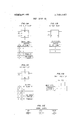
- FIGS. 1A and 1B depict a simplified block diagram of one specific illustrative embodiment of the invention and show the manner in which modules may be crossconnected;
- FIG. 2 shows the system clock decoder for a station module
- FIG. 3 shows a circuit for controlling the exchange of intermodule signals between a station module and connected service modules
- FIG. 4 shows a signal receiver and store for data signals forwarded by a station set
- FIG. 5 shows a switching network for connecting a line from the station set to any cross-connected line module
- FIG. 6 shows a switch-hook time-out circuit, a data transmitter and the function calculator
- FIG. 7 shows a button code register and a memory register
- FIGS. 8 and 9 show the circuitry of line module
- FIG. 10 shows various feature modules
- FIGS. 11A to 11H describe the drawing conventions for gates, multiplexers, decoders, and flip-flops, together with truth tables therefor;
- FIG. 12 shows the manner in which FIGS. 2-7 are to be arranged
- FIG. 13 shows the manner in which FIGS. 8-10 are to be arranged
- FIG. 14 shows the arrangement of FIGS. 1A and 1B.
- the major elements of this embodiment of the invention include station modules 4, 5, and 6 associated with respective station sets 1 and 2 and call director" set 3; line modules 9 and 10 associated with separate lines from a central office or Private Branch Exchange (PBX); and a service designation field 15 through which modules are interconnected.
- PBX Private Branch Exchange
- service modules such as privacy module 11, hold module 12, exclusion module 13, and message waiting module 14.
- the whole arrangement is controlled by multi-phase system clock 7 which generates program controlled instruction signals on the A DATA BUS and the B DATA BUS.”
- station sets 1 and 2 are each provided with six non-locking push buttons, any one of them can be assigned to a particular line, or feature, module.
- station module 4 the following illustrative assignment is shown: buttons 1 and 2 to C.O./PBX lines (modules 9 and 10), and button 6 to the privacy feature (module 11).
- Station set 2 as may be seen by reference to station module 5 has button 1 assigned to the same line (module 10) as button 2 of set 1, button 2 to the exclusion feature (module 13), and button 6 to the message waiting feature (module 14).
- Button 1 of set 3 is associated with the same line (module 9) appearing at button 1 of set 1, and button n of set 3 controls the message waiting feature (module 14).
- Button positions of a station set are associated with particular lines by interconnecting the line module for each of the lines with the associated station module using four wires -two of the wires designated T and R are for the voice transmission and the other two wires shown with arrowheads are for intermodule signalling.
- a single pair of wires is ncessary to cross-connect the button position of the station module with a feature module. It is to be noted that with the exception of the message waiting module 14, only a single feature module, modules 11-13, is required to serve the entire system and provide the feature service to all station sets.
- Station sets 1 and 2 and call director set 3 connect to separate station modules 4, 5, and 6 via a six-wire path.
- Conductors T and R of that path form a conventional voice path and the remaining two pairs of conductors are for sending and receiving lamps, ringer, button depression and switch-hook status data signals.
- the circuitry (not shown) of station sets 1 ane 2, and of set 3 responds to bipolar signals on the data channels for updating the lamps and ringer indication of the set, converts the received signals and returns to station modules 4, 5, and 6 bipolar encoded signals representing the button and switch-hook status at the set. Power for operating the station set circuitry is supplied over the data channels.
- Multi-phase system clock 7 comprises a semipermanent memory for storing a list of program instruction signals as well as signal sending equipment for one-at-a-time transmission of the stored signals, or words, in a binary encoded format via A DATA BUS and B DATA BUS.”
- the circuitry (not shown) of clock 8 is conventional and may comprise, for example, a drum-type memory, a drum scanner circuit and a sig nal transmitter coupled to the scanner circuit.
- Each instruction, or word comprises seven bits which are forwarded in parallel on conductors AO-A6 and B0-B7 and received at all modules simultaneously.
- a service input/output intermodule signal sending an receiving circuit Each of the above circuits may be combined and controlled to operate in any one of various sequences by program instructions on the A DATA BUS. Moreover, the circuit operations performed by each individual circuit may be altered and directed by the same instructions.
- One of the most significant circuits of the station module is the function calculator which expands the operational range of station modules 4, 5, and 6 in response to program signals.
- the calculator is connected to eight internal circuit variables (circuit conditions); and upon appropriate instructions, it can serially select a series of these variables and perform combinatorial logic thereon. These variables can be derived from connected service modules to expand the possible circuit conditions which can be logically combined. As a result, many operations can be facilely programmed and new service conditions accommodated by simple program changes.
- Line modules also respond to program instruction signals on the B DATA BUS" for updating supervisory, hold and A lead information.
- This module is equipped with various timing devices for timing the interval between ringing signal bursts, the interval after receipt of the first ringing signal burst (delayed ringing. and the interval following receipt of an on-hoolt signal while on hold for controlling the release of the line module.
- Feature modules such as the Privacy, Hold and Exclusion Modules 11, 12 and 13, contain coded gates which control the transmission of a signal to connected station modules upon receipt of a special program instruction.
- the transmitted signal is sent at various times during the program and its interpretation is dependent upon the sub-routine group of instructions of which the special program instruction is a part.
- FIGS. 11A, 11B, 11C and 11D disclose the details and respective symbols for each logic gate and flip-flops employed in the system.
- FIG. 11A The truth table for a J-K type flip-flop is shown in FIG. 11A.
- Positive going transient pulses on terminal T referred to ordinarly as toggle pulses, activate the flipflop into different states depending upon the level of the signals on terminals J AND K. If the state of terminals J and K are (I) when the toggle voltage is applied to terminal T, the flip-flop switches so as to form the complement of the previously stored signal. The latter is indicated in the truth table as a 6.
- Terminals PS and PC asynchronous inputs, respectively set and clear the flip-flop to establish initial states. Additional details of the operation of a J-K fliop-flop may be obtained by reference to Logic Design of Digital Computers, by Montgomery Phister, Jr., page 128 et seq.
- a D type flip-flop is activated by toggle pulses at terminal T to produce the outputs at terminal 1 indicated in the truth table of FIG. 118. It may be seen the level at terminal D is reflected without inversion at terminal 1 and complemented at terminal 0. See the aforementioned text by Montgomery Phister, Jr., page 126.
- a S-C flip-flop logically functions in the same manner as a J-K flip-flop with one important difference. If zeroes appear at terminals S and C concurrent with a toggle voltage at terminal T, the complement of the previously stored signal in the flip-flop is formed at its output terminals 0 and 1. From reference to the truth table in FIG. 11C this may be readily seen.
- a multiplexer is a device controlled by an octal code at its terminals A, B, and C for connecting any one of its terminals 0 7 to terminal D.
- the relationship between the octal code, in binary form, and the terminal connected to terminal D is shown in the accompanying table.
- FIG. 11H discloses the symbol and truth table for a binary code controlled multiplexer.
- a shift register such as the one shown in FIG. 11D, stores binary coded signals.
- the binary signals appearing at terminal D are shifted" into the cell marked 1, one at a time, for each positive going pulse appearing at terminal T.
- the previously stored binary signal is shifted into cell 2 and from thence into cell 3.
- the vertical lines shown connected to cells 1-3 represent the outputs of each cell.
- An Octal Decoder forms a 1 signal at its output terminals 1-8 in accordance with octal encoded signals at terminals A, B, C, and D.
- outputs at terminals l 8 are zero; and upon the occurrence of a predetermined octal binary code at terminals A, B, and C, one of the terminals 1-8 is high (l).
- Terminal D is effectively used for inhibiting signals. The presence of acne at terminal D raises the octal code equivalent above the number 8, and thus there is no output.
- I signals are used to enable or to activate circuits.
- the symbolic convention used is a dot. This dot may be shown at the intersection of an input lead and gate, or output lead and gate.
- AND gate 97 has an inversion symbol at its output; thus a one signal at its input will produce a zero signal at the input of the succeeding gate 96.
- Inversion symbols are also used on decoders, multiplexers, and shift registers; and when so used, their meaning is consistent with the above description.
- STATION MODULE (FIGS. 2-7) This module is the-focal point for operations within the system because it provides an interface between a telephone set and various service modules including line modules.
- the majority of the logic control circuitry The first sub-circuit of the station module which we will consider is the system clock decoder 39 shown entirely in FIG. 2. It functions to decode in a predetermined manner the binary data on leads A0-A6 for controlling local module circuits.
- the main purpose of decoder 39 is to reduce the number of leads in the A bus. Buffer circuits 30-36, each including a line isolator and amplifier, are inserted between the A bus connection and the logic gates of decoder 39.
- the isolator which may typically be a diode or transistor junction, prevents false signals generated within the module circuitry from becoming impressed on the A bus leads and thereby rendering all modules tied in common to this same bus inoperative.
- the amplifier also increases the signal level of the voltage applied on leads A0-A6.
- the system decoder essentially comprising and gates wired together in a particular pattern to translate received word signals on leads A0-A6 into signals on various leads shown exiting at the top, right-side and bottom of FIG. 2.
- Octal Decoders 37 and 38 are controlled by clock signals applied to their respective terminals A, B, and C for generating a signal on one of the leads in cable 110.
- the respective terminals D of decoders 37 and 38 always contain the logical compliment with respect to each other of the derived signals. Thus, in effect, when decoder 37 is inhibited, decoder 38 is enabled and vice-versa.
- FIG. 4 it depicts a Data Receiver 50 and a Data Register 53 for detecting and recording information transmitted from the station set, Station sets transmit bipolar pulses (a sample shown in the figure) which are received at terminal IN of converter 52.
- Converter 52 generates a clock signal derived from the transmitted bipolar signals, which clock signal is forwarded on lead 106 to Data Register 53 for synchronizing the circuit operations with the incoming pulses.
- Converter 52 also converts and separates the bipolar pulses into separate unipolar pulses shifting between level 0 (ground) and level 1 (positive level).
- the separated signals are connected via leads 107 and 108 to terminals S and C (set and reset) of flip-flop 51. In this manner, each negative going pulse resets and each positive going pulse sets the state of flip-flop 51.
- the incoming bipolar pulses are received by a transformer 20 which couples the signal to gate circuitry comprising transistors 21 and 22.
- Transistor 21 is conducting on positive pulses and transistor 22 is conducting on negative pulses.
- the station set forwards a seven-bit word which indiates the status of the switch hook and six buttons located in the base of the set.
- the right-most bit of the transmitted word corresponds to the switch hook bit.”
- the received data is recorded in the same order as transmitted, in data register 53. For purposes of this present illustration, it will be assumed that the data is transmitted in the following order: Switch hook bit, status of button 6, button 5, button 4, button 3, button 2, and button 1.
- the center tap of the input winding of transformer 20 is connected to negative battery.
- center tap of transformer 79 having windings connecting to the station set, connects to positive battery.
- the station set equipment is powered over the same channels as signals are transmitted and received. Due to the winding orientation of transformers 20 and 79, the flux created by the DC current flow is cancelled out in the primary windings. Thus the transformer does not saturate and the signals transmitted are not distorted.
- the circuitry of Data Receiver 50 and Data Register 53 are combined logically to perform two separate operations.
- data transmitted by the station set is converted into unipolar information by receiver 50 and compared in register 53 against the information previously transmitted by the station set and presently recorded in shift register 56. This operation is performed to determine a change of state of any button at the station set.
- the second operation which can be performed by the combined circuitry of receiver 50 and register 53 is the location of a I bit stored in register 56. This operation is performed when it is desired to identify the specific button having a change of state.
- the station set forwards a 7-bit word denoting the status of the switch hook and the six buttons at the set.
- a seven bit signal which comprises all s. Recall that the receipt of a 1 bit signal denotes a button depression; and ifit is received at the beginning of the bit stream. it denotes an off-hook state. Accordingly, the assumed state, all 0s, indicates an idle condition of all buttons and an onhook state of the switch hook.
- the output (terminal I) of flip-flop 51 may be coupled to terminal D of register 56 by multiplexer 55.
- the system program decoded by decoder 39 provides a signal on lead 101 such that multiplexers 55 and 58 are toggled to 0.
- syn chronizing clock pulses on lead 106 are coupled to register 56 resulting in the shifting of the data from left to right, or from cells 1 to 7.
- each stored unit, in the present example 05 is coupled to lead 100 and to Exclusive OR gate 54.
- the received data, converted to unipolar information is coupled by a lead 109 to gate 54 and therein compared.
- gate 54 forwards a signal via OR gate 59 to set flip-flop 57.
- the signals on lead 109 are also coupled via multiplexer 55 to register 56 for storage therein. It is to be noted that the registration ofa mismatch in flip-flop 57 and the shifting of the register information in register 56 are controlled by the derived clock signals which toggle those devices. Thus as the priorly stored information in register 56 is shifted out of register 56 and connected to lead 100, the incoming data is stored in its place.
- the circuitry of Data Receiver 50 and Data Register 53 can also be used to locate the bit position of a l stored in register 56. It will be recalled that a 1 corresponds to the off-hook state of a switch hook or a button depression signal.
- a program instruction manifest by a particular word appearing on leads AO-A6 controls a signal level in FIG. 4 ofleads 101, 102, and 104.
- the signal level on lead 101 toggles multiplexers 55 and 58 to a 1.
- the incoming data which may or may not be transmitted by a station set at the time that this operation is initiated, is blanked, or set to 0, by the signal level on lead 102 which maintains flip-flop 51 in the reset, clear, state. Setting the incoming data to zero is necessary to prevent the unwanted input signals from interfering with this operation.
- the search for the one bit in a word stored in register 56 is initiated by a shift clock pulse which is continuously available on lead 103 and by an enabling signal on lead 104.
- the shift clock signals are comparable to those of the derived clock signals priorly discussed on lead 106. They are gated by multiplexer 58 into the register. 56 causing the stored information to be coupled onto lead 100. Since this shifting process is destructive, the original signals are recriculated through multiplexer 55 and returned for storage in register 56.
- flip-flop 51 is clamped effectively in a reset state, a 0 level signal appears on lead 109 and that signal is compared against the information on lead by Exclusive OR gate 54. Thus a 1 bit will be detected as a mismatch and gate 54 will transmit a signal via gate 59 and reset flip-flop 57.
- the foregoing operation is ordinarily coordinated with a separate circuit action carried on in the button register 40 shown in FIG. 7.
- a signal appears on lead which may be traced from terminal 1 of flipflop 57, FIG. 4, to gate 45 of register 40. This signal halts the shift register operation at the last code registered in register 42 before a mismatch is detected.
- Each station set button is identified by a unique bi nary code as follows:
- Button Code Word 2 000 (Prime Line) 3 001 4 Oll EXP. (N.C.) lll VACANT 010
- the code associated with button 2 is 000. It also corresponds to the state of the module circuitry during a power failure so that, as will be explained in more detail hereinafter, the prime line is automatically connected to a line module during such a failure.
- FIG. 7 discloses two 3-bit shift register arrangements which are essentially used in the determination and storage of codes relating to station set buttons.
- the data, or button number may be serially shifted between button register 40 and memory register 46.
- Information is shifted from button register 40 to register 46 under control of multiplexer 48 and the signal level on leads 112, 113, 114 and 139.
- the signal levels on these leads are established by decoder 39 in accordance with a program instruction signal received on leads A0A6.
- Gate 45 of Register 40 is turned on by the presence of 0 signal, a mismatch signal, on lead 105 and in succession, OR gate 44 and gate 43 is enabled.
- Gate 44 is enabled by the combination of l signal at the output of gate 45 and a 1 signal on lead 114.
- the latter signal is derived from the program instruction.
- Lead 103 connects to gate 43 and conveys clock pulses.
- the pulsing output of gate 43 acts as a toggle signal and the information in register 42 is shifted bit by bit from cell 1 to 3.
- the output of cell 3 is coupled via lead 111 and multiplexer 48, and recorded in register 47.
- multiplexer 48 is switched by the signal level on lead 112 so that terminal 1 is internally connected to terminal D.
- terminal T of register 47 is pulsed by the clock pulses on lead 103 via gate 49 for shifting register 47 and recording the output of register 42.
- register 47 can be circulated; i.e., output and input of register connected together, in a manner similar to the operation previously described for shift register 56 of Data Register 53.
- Multiplexer 48 if toggled to O, in accordance with an instruction signal on lead 112, couples the output of the right-most cell, cell 3, of shift register 47 to the left-most cell, cell 1, of that same register.
- Application of toggle signals at terminal T circulates the stored information bit by bit.
- register 47 While the information stored in register 47 is being circulated, it can also be recorded in register 42 of Button Register 40. If multiplexer 41 is switched by a signal on lead 113 so that internally terminal 1 and D are interconnected, the circulated pulses are conveyed via lead 168 and the Multiplexer 41 to terminal D of register 42. The concurrent application of toggle signals at terminal T shifts the circulated date and stores it bit by bit.
- the service input-output circuit 66 shown in FIG. 3 functions to send and receive intermodule signals via leads 121-132.
- station set buttons l-6 may be associated with any service designation field.
- FIGS. 1A and IE will assist in recalling how these cross-connections are made.
- Crossconnections are made between conductors 121-132 shown at the top center of FIG. 3 and service modules. For each service module associated with a particular station set button, two wires must be connected from the station module to the service module. In FIG. 3, the numbers 1-6 in line drivers 91 and line receivers 92 correspond to the button position of the station set. If, for example, it is desired to assign button 2 to a particular service, conductors 122 (outgoing data) and 128 (incoming data) are connected to the service module capable of performing the service.
- the particular interconnected module with which the station module communicates via the circuit of FIG. 3 is controlled by the button code stored in Button Register 40 (FIG. 7) and also by execute signals derived by Decoder 39 from program instruction signals on leads A-A6 (FIG. 2). Signals representative of a stored button code are forwarded via cable 119 over the leads of that cable which are designated AB, BB, and CB.
- the binary code assigned to each button has been selected so that the storage of the button code corresponding to station button No. 1 in shift register 42 and the recirculating of the cell 3 binary bit will cause the generation of all button codes. Importantly, these codes will be generated in succession starting with button No. 1 and ending with button No. 6. Thus when it is necessary to transmit data to the station set, a program sequence is initiated whereby the button register 40 transmits facilely and in serial form, control signals to circuit 66 for interrogating one at a time each service module associated with each button.
- conductor 118 shown to the left-hand side of FIG. 3 conveys a l or 0 bit.
- a I bit controls circuit 66 so that intermodule signals are exchanged only with one service module as determined by the code stored in Button Register 40. If a 0 bit occurs on conductor 118, signals are exchanged concurrently with all cross-connected service modules. The importance of these operations will be more apparent from a consideration of programs and their functions. For purposes of the ensuing discussion, let it be assumed that the signal level on conductor 120 (R bit) does not inhibit the operation of gates 95 and 96. v
- Decoder 90 decodes the octal signals on leads AB, BB, and CB into a one-out-ofn code signal which is applied to one of the terminals 1-6.
- the enabled one of the gates 98 signals with a I, one of the line drivers 91 and one of AND gates 99.
- an intermodule signal received via the associated of the line receivers 92 is coupled to OR gate 94 and stored in flip-flop 93, T bit" flip-flop. It should be noted that a toggle pulse on lead 117 is required to store signals in T bit flip-flop 93. This pulse is controlled through program instructions.
- decoder 90 When it is desired to send and receive intermodule signals simultaneously over all intermodule signal channels, decoder 90 is inhibited by a 1 signal at terminal D. It will be recalled that a 0 signal is conveyed on conductor 118 to initiate this operation, and it is coupled to inhibit decoder 90 via NAND gate 95. The outputs at terminals 1-6 of decoder 90 are therefore all 0, inverted to 1'5.
- the 0 signal on lead 118 also produces a 0 signal on lead 169 via gates 97 and 96.
- the inputs to all gates 98 from decoder 90 are 15 and their outputs after inversion are ls. In this mode all received intermodule signals are logically combined in OR gate 94 and the output is stored in flip-flop 93.
- the intermodule signalling arrangement of FIG. 4 has a more meaningful significance when it is realized that intermodule signals are exchanged at prescribed times during a program sequence. Thus the fact that such a signal exchange has occurred is significant and meaningful only if the program sequence being run at the time of the exchange is considered.
- An example of the utilization of intermodule signals in coordination with program instructions may demonstrate the versatility of the signalling arrangement. It may be noticed that station modules do not have memory devices for registering the various types of service modules to which they are cross-connected. When such information is required, a special program sequence is initiated and instructions are transmitted to all modules requesting that all modules of a certain type transmit intermodule signals Station modules, upon receipt of the same instruction signal, arrange the input-output circuit of FIG.
Abstract
A program controlled key telephone system is disclosed. The system includes line modules and station modules which respectively provide the interface circuitry between PBX/CO lines and station set equipment. Modules are connected to a multi-phase clock which generates a reiterative list of binary coded instruction signals for directing circuit operations. Each of the modules acts simultaneously on receipt of the instruction signals to generate independently and dynamically separate work programs for each module. In addition, intermodule signals are exchanged during various subroutines in the program as directed by the simultaneously received instruction signals at each module.
Description
Write States atent n 1 lfinollman et a1.
MODULAR KEY TELEPHONE SYSTEM HAVING A DISTRIBUTED PROCESSOR ORGANIZATION Inventors: Dieter John Henry Knollman,
Guttenberg, N.J.; James Louis Simon, Denver, Colo.
Assignee: Bell Telephone Laboratories,
Incorporated, Murray Hill, Berkeley Heights, NJ.
Filed: Oct. 1, 1971 Appl. No.: 185,523
Related US. Application Data [62] Division of Ser. No. 43,812, June 5, 1970, Pat. No.
[52] US. Cl. 179/99 [51] Int. Cl. H04m 3/22 [58] Field of Search 179/99, 81 R, 2 DP, 179/18 ES,18 AD [56] References Cited UNITED STATES PATENTS 3,244,815 4/1966 Anderson et a1v 179/99 3,385,935 5/1968 Anderson et al. 179/99 3,519,757 7/1970 Anderson et all. 179/99 3,549,820 12/1970 Knollman 179/81 R Primary Examinerl(athleen H. Claffy Assistant Examinerl(enneth D. Baugh Att0mey-W. L. Keefauver et a1.
[57] ABSTRACT A program controlled key telephone system is disclosed. The system includes line modules and station modules which respectively provide the interface circuitry between PBX/CO lines and station set equipment. Modules are connected to a multi-phase clock which generates a reiterative list of binary coded instruction signals for directing circuit operations. Each of the modules acts simultaneously on receipt of the instruction signals to generate independently and dynamically separate work programs for each module. In addition, intermodule signals are exchanged during various subroutines in the program as directed by the simultaneously received instruction signals at each module.
16 Claims, 22 Drawing Figures STATION MODULES (FIGS 2-7) id) KEVI DA TA STATION T MODULE T CHANNEL PAIENIEUJUL3 1 ma 3, 749 848 sum 01 or I3 STATION MODULES FIG. IA IR KEY I I (FIGS. 2-7) STATION I DATA CHANNEL A0 Abl DOD DOD
IIII+ 2 (FIGS. 2-7) BELL I RR 1 sTATloN T R I l MODULE I fgill IIII DATA CHANNEL A DATA BUS (FIGS. 27)
STATION MODU E I L }KEV n I DATA CHANNEL +IIII SERVICE MODUL SHEET 02 0F 13 PAIENIED JUL31 I975 FIG. 18
MULTIPHASE SYSTEM CLOCK TO OTHER KEY SYSTEMS PATENIEUJUL31 ms I I 749 848 snm 03 or 13 SYSTEM CLOCK DECODER F IG. 2
EXECUTE OPERATION PATENIED 3.749.848
J-K FLIP-FLOP 0 FLIP-FLOP 'J PS I -o K A T 0 PC QT TRUTH TABLE w; oUTPUT OUTPUT K AT TERM 1" AT TERM I o I o 0 1 6(T0GGLE) NO sTATE O O Q (CHANGE) F/G.//C
s-c FL|P-FLOP 5 PS T FIG/ID SHIFT REGISTER C PC 0 I OUTPUT OUTPUT b l INPUT DATA AT M (k J) S C TER I TOGGLE 2 1 o o SIGNAL T NO STATE Q CHANGE o 0 5 (ToGGLE) FIG //5 LOGIC GATES OR AND NAND PAIENIEU JUL 3 I I915 sum 1: ur 13 FIG. IIF
OCTAL CODE ENABLE SIGNALS (INHBIT) TRUTH TABLE FOR ALL DECODERS EXCEPT DECODER 90 TRUTH TABLE FOR DECODER 90 OUTPUT SIGNAL AT TERMINAL 7 NOT USED 0 8 NOT USED ENABLE SIGNALS FIG l/H MULTIPLEXER A s I I FIG llG MULTIPLEXER ENABLE SIGNALS l U P T U o DTO ENABLE SIGNALS |I( :IPUT TERM. N0.
INPUT TERM. NO.
NECTED TO TERM. D
ENABLE SIGNALS A B c CON MODULAR KEY TELEPHONE SYSTEM HAVING A DISTRIBUTED PROCESSOR ORGANIZATION This application is a division of application Ser. No.
43,812, filed June 5, 1970, now US. Pat. No.
BACKGROUND OF THE INVENTION 1. Field of the Invention This invention concerns a communication system which comprises a plurality of distributed data processor units and a common instruction word generator for dispensing instruction signals in accordance with a master program to direct the system operations. More particularly, it concerns an arrangement in which such units operate simultaneously on received instructions to dynamically develop subprograms, or work programs, for controlling the signal processing of received telephone data, and transmission of such data between units and to peripheral circuitry. A particular aspect of the invention concerns utilization of these data processing techniques in a key telephone communication arrangement.
2. Prior Art Business and resident subscribers requiring access to more than one telephone line have been equipped according to one of a number of so-called standard wiring plans." Each plan relates to a different operating feature, such as the ability to pick up any one ofa number of central office, private branch exchange (PBX), or intercommunicating lines, to originate or answer calls on such lines and to hold one line while another line is seized for use. The increased diversity of these wiring plans subsequently led to a coordination of designs which today is characterized as key system equipments primarily because most of the operational features are controlled from keys mounted on the face of a relatively samll desk or table-mounted station set. Typically, a modern key telephone station set includes line pick up and holding keys, as well as signaling lamps in the base of the telephone set.
Modern key system arrangements provide for a variety of special customer services of varying degrees of complexity. Guided by past developments, it is now increasingly apparent that the feature services of todays systems probably will not meet the expanding service requirements of the immediate future. This problem has been met in the past by furnishing additional equipment space for expansion, extra cross-connection facilities and unused conductors in the cable runs. This approach has proven to be inefficient, economically unsound, and in many instances, inadequate for the service expansion.
As those familiar with key telephone systems are well aware, one of the most tedious and time-consuming installation items is the connection of individual station sets to key system common equipment and the wiring of service options. Even though as many conductors as possible are normally multiplied at various points near the station sets, there are still large numbers of internal circuit connections to be made, since each line appearance and service feature at a station set requires individual attention and connection.
This problem has been recognized in the past and to some degree solved by the provision of key telephone station line concentrators. Concentrators reduce the number of key system conductors between station sets and system equipment by connecting each station set ous internal key equipment units and for simplifying subsequent engineering design effort required to efficiently make circuit modifications for the almost predictable system rearrangements.
SUMMARY OF THE INVENTION The aforementioned problems of providing an economical rearrangeable key telephone system are overcome by the novel application of modularization techniques and program controlled telephone data processing to key telephone systems. The key telephone common equipment is separated into functional units, modular units, each embodying separate data processor capabilities. All functional units connect in parallel to an instruction code bus on which a reiterative seven-bit wide data stream is transmitted. The data stream is de coded from a single master program, and it directs con currently individual module operation as well as the intermodular signaling.
Each line from a central office (CO) or PBX has one functional unit associated therewith called a line module. A separate functional unit termed a station module is associated with individual station sets. Various other functional units are also provided for special service features-such as, privacy, holding, exclusion, and message waiting.
Although each module receives simultaneously the same instruction signals from the word generator, each module responds to the signals in a different manner. Every module contains a decoder for deriving internal control signals from the instruction signals. Each different type of module has its own special decoder. Although the decoders of line modules are alike, they are distinctly different from those of station modules and other service modules.
The circuit response of each module to the instruction signal is also different because of memory updated by a function calculator which is provided in station modules. The calculator is controlled by program instruction signals and is capable of altering the circuit response of a station module, or modules connected thereto, on receipt of what is termed conditional program instruction signals. Each calculator is capable of performing under program instructions a combinatorial logic function of any number of variable circuit conditions presented to it. Data relating to such conditions can be sent via intermodule signaling channels so that functions relating to service modules can be solved by the station module and returned to the service modules. The solution of functions solved by the calculator is used to generate effectively new program instruction signals at each module from the received master instruction signals. Accordingly, each module has the independent facility of adjusting its operation dynamically to changing circuit conditions or environmental data. Moreover, the utilization of the calculator and its associated memory reduces the number of discrete memory devices required by each module.
The assignment of C.O./PBX lines to the keys of a station set is made by wiring, or cross-connecting line modules to the associated station module. Similarly, service features controlled by keys at a station set are provided by wiring service modules to the associated station module. Importantly, the interrnodule wiring is simplified and uniquely patterned in our arrangement so as to minimize the engineering and installation efforts required. Signaling between modules (intermodule signaling) is carried on by way of a two-wire data channel, which comprises the interconnection wiring. The only other cross-connect wiring required is that of a voice transmission channel between special units-such as between a station module and line module. As a result of the simplification of the intermodule wiring, our arrangement requires less time and expertise to engineer, can be changed with minimum service interruptions when system reorganization is demanded by customer needs, and enables new features, packaged as modular function units, to be added simply to the system without extensive rewiring.
The system is organized on a per line, per station set and per feature basis, thereby allowing the initial installed cost to be low. The system may easily grow, however, by the addition of individual modules to add lines, station sets, or new featurs. Modules act concurrently on program instruction signals and thus the addition of standard modules does not require changes in program or interpose delay in the system operation. In addition, the simultaneous module operation enables new features to be added by program change because there is adequate reserve time-wise in the basic program format. Since the majority of circuit operations takes place in discrete modules rather than in common circuits, the reliability of the system is high because component failure in any module will at most affect only a single line, station set or feature service.
The operation of each modular unit is controlled and time-wise synchronized by a multi-phase system clock, also referred to as the word generator, which sends clock signals over a seven-wire bus. In our arrangement, the bus is divided into an A and B bus for preservation of minimum signal levles and for circuit operating integrity. The system clock applies the same signals concurrently to both busses. Under control of these signals station modules concurrently scan station sets and exchange information with connected service modules. In addition, service modules respond to the signals to initiate independent circuit action and to send signals to station modules for updating the lamp indications. The program instructions, in order, direct station modules to:
1. send control information to stations sets defining the line and ringer activity,
2. receive and store control information pertaining to the switch-hook and button status at all station modules,
3. scan received data for changes of state and act upon it, and
4. interrogate and update all connected service modules.
Line modules, as well as other service feature modules, are also commanded at various times during the program by these signals to identify themselves to connected station modules, to give the supervisory or hold status of the module, to store special service marks such as privacy and exclusion, and to exchange this information with other modules as the program directs.
The objects, features and advantages of this invention wil be more clearly understood from a reading of the following description of an illustrative embodiment.
BRIEF DESCRIPTION OF THE DRAWING FIGS. 1A and 1B depict a simplified block diagram of one specific illustrative embodiment of the invention and show the manner in which modules may be crossconnected;
FIG. 2 shows the system clock decoder for a station module;
FIG. 3 shows a circuit for controlling the exchange of intermodule signals between a station module and connected service modules;
FIG. 4 shows a signal receiver and store for data signals forwarded by a station set;
FIG. 5 shows a switching network for connecting a line from the station set to any cross-connected line module;
FIG. 6 shows a switch-hook time-out circuit, a data transmitter and the function calculator;
FIG. 7 shows a button code register and a memory register;
FIGS. 8 and 9 show the circuitry of line module;
FIG. 10 shows various feature modules;
FIGS. 11A to 11H describe the drawing conventions for gates, multiplexers, decoders, and flip-flops, together with truth tables therefor;
FIG. 12 shows the manner in which FIGS. 2-7 are to be arranged;
FIG. 13 shows the manner in which FIGS. 8-10 are to be arranged; and
FIG. 14 shows the arrangement of FIGS. 1A and 1B.
GENERAL DESCRIPTION As seen in FIGS. 1A and 1B, the major elements of this embodiment of the invention include station modules 4, 5, and 6 associated with respective station sets 1 and 2 and call director" set 3; line modules 9 and 10 associated with separate lines from a central office or Private Branch Exchange (PBX); and a service designation field 15 through which modules are interconnected. Various services are provided by service modules such as privacy module 11, hold module 12, exclusion module 13, and message waiting module 14. The whole arrangement is controlled by multi-phase system clock 7 which generates program controlled instruction signals on the A DATA BUS and the B DATA BUS."
In this embodiment of the invention wherein station sets 1 and 2 are each provided with six non-locking push buttons, any one of them can be assigned to a particular line, or feature, module. Referring to station module 4, the following illustrative assignment is shown: buttons 1 and 2 to C.O./PBX lines (modules 9 and 10), and button 6 to the privacy feature (module 11). Station set 2, as may be seen by reference to station module 5 has button 1 assigned to the same line (module 10) as button 2 of set 1, button 2 to the exclusion feature (module 13), and button 6 to the message waiting feature (module 14). Button 1 of set 3 is associated with the same line (module 9) appearing at button 1 of set 1, and button n of set 3 controls the message waiting feature (module 14).
Upon closer examination of the service designation field 15, it may be observed that a simplified wiring pattern emerges. Button positions of a station set are associated with particular lines by interconnecting the line module for each of the lines with the associated station module using four wires -two of the wires designated T and R are for the voice transmission and the other two wires shown with arrowheads are for intermodule signalling. To assign a feature operation to a button, a single pair of wires is ncessary to cross-connect the button position of the station module with a feature module. It is to be noted that with the exception of the message waiting module 14, only a single feature module, modules 11-13, is required to serve the entire system and provide the feature service to all station sets.
Station sets 1 and 2, and call director set 3 connect to separate station modules 4, 5, and 6 via a six-wire path. Conductors T and R of that path form a conventional voice path and the remaining two pairs of conductors are for sending and receiving lamps, ringer, button depression and switch-hook status data signals. The circuitry (not shown) of station sets 1 ane 2, and of set 3 responds to bipolar signals on the data channels for updating the lamps and ringer indication of the set, converts the received signals and returns to station modules 4, 5, and 6 bipolar encoded signals representing the button and switch-hook status at the set. Power for operating the station set circuitry is supplied over the data channels.
Considering now the circuitry of station modules 4, 5, and 6 in greater detail, it comprises:
a. a system clock decoder,
b. an incoming data register,
c. a function calculator,
d. an outgoing data transmitter,
e. a switching network,
f. a switch-hook and time-out circuit,
g. a button code and memory register, and
h. a service input/output intermodule signal sending an receiving circuit. Each of the above circuits may be combined and controlled to operate in any one of various sequences by program instructions on the A DATA BUS. Moreover, the circuit operations performed by each individual circuit may be altered and directed by the same instructions. One of the most significant circuits of the station module is the function calculator which expands the operational range of station modules 4, 5, and 6 in response to program signals. The calculator is connected to eight internal circuit variables (circuit conditions); and upon appropriate instructions, it can serially select a series of these variables and perform combinatorial logic thereon. These variables can be derived from connected service modules to expand the possible circuit conditions which can be logically combined. As a result, many operations can be facilely programmed and new service conditions accommodated by simple program changes.
Line modules also respond to program instruction signals on the B DATA BUS" for updating supervisory, hold and A lead information. This module is equipped with various timing devices for timing the interval between ringing signal bursts, the interval after receipt of the first ringing signal burst (delayed ringing. and the interval following receipt of an on-hoolt signal while on hold for controlling the release of the line module.
Feature modules, such as the Privacy, Hold and Exclusion Modules 11, 12 and 13, contain coded gates which control the transmission of a signal to connected station modules upon receipt of a special program instruction. The transmitted signal is sent at various times during the program and its interpretation is dependent upon the sub-routine group of instructions of which the special program instruction is a part.
DISCRETE LOGIC CIRCUITS The presently disclosed system makes extensive use of Diode Transistor Logic (DTL) and Resistor Transistor Logic (RTL) in which single transistor stages are used as an inverter, an AND gate, or an OR gate, depending upon the nature of the input signals applied thereto and the functions to be performed by this stage. FIGS. 11A, 11B, 11C and 11D disclose the details and respective symbols for each logic gate and flip-flops employed in the system.
The truth table for a J-K type flip-flop is shown in FIG. 11A. Positive going transient pulses on terminal T, referred to ordinarly as toggle pulses, activate the flipflop into different states depending upon the level of the signals on terminals J AND K. If the state of terminals J and K are (I) when the toggle voltage is applied to terminal T, the flip-flop switches so as to form the complement of the previously stored signal. The latter is indicated in the truth table as a 6. The presence of zeroes at terminals J and K concurrent with a toggle voltage at terminal T causes the flip-flop to remain in its original state. Terminals PS and PC, asynchronous inputs, respectively set and clear the flip-flop to establish initial states. Additional details of the operation of a J-K fliop-flop may be obtained by reference to Logic Design of Digital Computers, by Montgomery Phister, Jr., page 128 et seq.
A D type flip-flop is activated by toggle pulses at terminal T to produce the outputs at terminal 1 indicated in the truth table of FIG. 118. It may be seen the level at terminal D is reflected without inversion at terminal 1 and complemented at terminal 0. See the aforementioned text by Montgomery Phister, Jr., page 126.
A S-C flip-flop logically functions in the same manner as a J-K flip-flop with one important difference. If zeroes appear at terminals S and C concurrent with a toggle voltage at terminal T, the complement of the previously stored signal in the flip-flop is formed at its output terminals 0 and 1. From reference to the truth table in FIG. 11C this may be readily seen.
Symbols for AND, NAND, and OR gates are shown in FIG. 11E. Truth tables for these gates are disclosed in the Phister text.
A multiplexer, FIG. 1 1G, is a device controlled by an octal code at its terminals A, B, and C for connecting any one of its terminals 0 7 to terminal D. The relationship between the octal code, in binary form, and the terminal connected to terminal D is shown in the accompanying table. FIG. 11H discloses the symbol and truth table for a binary code controlled multiplexer.
A shift register, such as the one shown in FIG. 11D, stores binary coded signals. The binary signals appearing at terminal D are shifted" into the cell marked 1, one at a time, for each positive going pulse appearing at terminal T. As each new signal is introduced into cell 1, the previously stored binary signal is shifted into cell 2 and from thence into cell 3. The vertical lines shown connected to cells 1-3 represent the outputs of each cell.
An Octal Decoder, FIG. 11F, forms a 1 signal at its output terminals 1-8 in accordance with octal encoded signals at terminals A, B, C, and D. In the idle state, outputs at terminals l 8 are zero; and upon the occurrence of a predetermined octal binary code at terminals A, B, and C, one of the terminals 1-8 is high (l). Terminal D is effectively used for inhibiting signals. The presence of acne at terminal D raises the octal code equivalent above the number 8, and thus there is no output.
Insofar as it has been possible, I signals are used to enable or to activate circuits. When it is necessary to form the inversion or complement of the signal, the symbolic convention used is a dot. This dot may be shown at the intersection of an input lead and gate, or output lead and gate. For example, in FIG. 3, AND gate 97 has an inversion symbol at its output; thus a one signal at its input will produce a zero signal at the input of the succeeding gate 96. Inversion symbols are also used on decoders, multiplexers, and shift registers; and when so used, their meaning is consistent with the above description.
DETAILED DESCRIPTION It is considered that the basic principles of the invention can best be introduced by considering the specific embodiment of the key telephone system having a distributed processor organization. The first consideration will be an analysis, module by module, of the logic circuits contained in each separate module. Next, the basic program instruction signals in the master program will be considered together with the related module circuit action. Following this, there will be presented a complete program for performing the operations of scanning lines and station sets, detecting line requests, and establishing call connections. The discussion also includes a special program instructions for feature operations.
STATION MODULE (FIGS. 2-7) This module is the-focal point for operations within the system because it provides an interface between a telephone set and various service modules including line modules. The majority of the logic control circuitry The first sub-circuit of the station module which we will consider is the system clock decoder 39 shown entirely in FIG. 2. It functions to decode in a predetermined manner the binary data on leads A0-A6 for controlling local module circuits. The main purpose of decoder 39 is to reduce the number of leads in the A bus. Buffer circuits 30-36, each including a line isolator and amplifier, are inserted between the A bus connection and the logic gates of decoder 39. The isolator, which may typically be a diode or transistor junction, prevents false signals generated within the module circuitry from becoming impressed on the A bus leads and thereby rendering all modules tied in common to this same bus inoperative. The amplifier also increases the signal level of the voltage applied on leads A0-A6.
The system decoder essentially comprising and gates wired together in a particular pattern to translate received word signals on leads A0-A6 into signals on various leads shown exiting at the top, right-side and bottom of FIG. 2. Octal Decoders 37 and 38 are controlled by clock signals applied to their respective terminals A, B, and C for generating a signal on one of the leads in cable 110. The respective terminals D of decoders 37 and 38 always contain the logical compliment with respect to each other of the derived signals. Thus, in effect, when decoder 37 is inhibited, decoder 38 is enabled and vice-versa.
Referring to FIG. 4, it depicts a Data Receiver 50 and a Data Register 53 for detecting and recording information transmitted from the station set, Station sets transmit bipolar pulses (a sample shown in the figure) which are received at terminal IN of converter 52. Converter 52 generates a clock signal derived from the transmitted bipolar signals, which clock signal is forwarded on lead 106 to Data Register 53 for synchronizing the circuit operations with the incoming pulses. Converter 52 also converts and separates the bipolar pulses into separate unipolar pulses shifting between level 0 (ground) and level 1 (positive level). The separated signals are connected via leads 107 and 108 to terminals S and C (set and reset) of flip-flop 51. In this manner, each negative going pulse resets and each positive going pulse sets the state of flip-flop 51.
The incoming bipolar pulses are received by a transformer 20 which couples the signal to gate circuitry comprising transistors 21 and 22. Transistor 21 is conducting on positive pulses and transistor 22 is conducting on negative pulses.
Before discussing in greater detail the operations of the remaining circuits disclosed in FIG. 5, it is opportune to first consider the nature of the signals forwarded by the station set. The station set forwards a seven-bit word which indiates the status of the switch hook and six buttons located in the base of the set. The right-most bit of the transmitted word corresponds to the switch hook bit." The received data is recorded in the same order as transmitted, in data register 53. For purposes of this present illustration, it will be assumed that the data is transmitted in the following order: Switch hook bit, status of button 6, button 5, button 4, button 3, button 2, and button 1.
The center tap of the input winding of transformer 20 is connected to negative battery. Referring momentarily to FIG. 6 and therein to Data Transmitter 70, it may be seen that center tap of transformer 79 having windings connecting to the station set, connects to positive battery. In this manner, the station set equipment is powered over the same channels as signals are transmitted and received. Due to the winding orientation of transformers 20 and 79, the flux created by the DC current flow is cancelled out in the primary windings. Thus the transformer does not saturate and the signals transmitted are not distorted.
Upon the receipt of appropriate program instruction signals, the circuitry of Data Receiver 50 and Data Register 53 are combined logically to perform two separate operations. In the first operation, data transmitted by the station set is converted into unipolar information by receiver 50 and compared in register 53 against the information previously transmitted by the station set and presently recorded in shift register 56. This operation is performed to determine a change of state of any button at the station set. The second operation which can be performed by the combined circuitry of receiver 50 and register 53 is the location of a I bit stored in register 56. This operation is performed when it is desired to identify the specific button having a change of state.
As noted previously, on each scan the station set forwards a 7-bit word denoting the status of the switch hook and the six buttons at the set. Let us assume that there is at present stored in shift register 56 a seven bit signal which comprises all s. Recall that the receipt of a 1 bit signal denotes a button depression; and ifit is received at the beginning of the bit stream. it denotes an off-hook state. Accordingly, the assumed state, all 0s, indicates an idle condition of all buttons and an onhook state of the switch hook. The output (terminal I) of flip-flop 51 may be coupled to terminal D of register 56 by multiplexer 55.
When it is desired to receive station set signals and compare those signals against the signals stored in register 56, the system program decoded by decoder 39 provides a signal on lead 101 such that multiplexers 55 and 58 are toggled to 0. Thus it may be seen that syn chronizing clock pulses on lead 106 are coupled to register 56 resulting in the shifting of the data from left to right, or from cells 1 to 7. As the data in register 56 shifts, each stored unit, in the present example 05, is coupled to lead 100 and to Exclusive OR gate 54. Concurrently, the received data, converted to unipolar information, is coupled by a lead 109 to gate 54 and therein compared. When a mismatch, or difference, between the compared signals occurs, gate 54 forwards a signal via OR gate 59 to set flip-flop 57. The signals on lead 109 are also coupled via multiplexer 55 to register 56 for storage therein. It is to be noted that the registration ofa mismatch in flip-flop 57 and the shifting of the register information in register 56 are controlled by the derived clock signals which toggle those devices. Thus as the priorly stored information in register 56 is shifted out of register 56 and connected to lead 100, the incoming data is stored in its place.
The circuitry of Data Receiver 50 and Data Register 53, as previously remarked. can also be used to locate the bit position of a l stored in register 56. It will be recalled that a 1 corresponds to the off-hook state of a switch hook or a button depression signal. To accomplish this operation, a program instruction manifest by a particular word appearing on leads AO-A6 controls a signal level in FIG. 4 ofleads 101, 102, and 104. The signal level on lead 101 toggles multiplexers 55 and 58 to a 1. In addition, the incoming data which may or may not be transmitted by a station set at the time that this operation is initiated, is blanked, or set to 0, by the signal level on lead 102 which maintains flip-flop 51 in the reset, clear, state. Setting the incoming data to zero is necessary to prevent the unwanted input signals from interfering with this operation.
The search for the one bit in a word stored in register 56 is initiated by a shift clock pulse which is continuously available on lead 103 and by an enabling signal on lead 104. The shift clock signals are comparable to those of the derived clock signals priorly discussed on lead 106. They are gated by multiplexer 58 into the register. 56 causing the stored information to be coupled onto lead 100. Since this shifting process is destructive, the original signals are recriculated through multiplexer 55 and returned for storage in register 56. As flip-flop 51 is clamped effectively in a reset state, a 0 level signal appears on lead 109 and that signal is compared against the information on lead by Exclusive OR gate 54. Thus a 1 bit will be detected as a mismatch and gate 54 will transmit a signal via gate 59 and reset flip-flop 57.
The foregoing operation is ordinarily coordinated with a separate circuit action carried on in the button register 40 shown in FIG. 7. As the bit information is shifted one at a time out of register 56, three digit binary codes are circulated in register 42 of button register 40. When a mismatch is detected, a signal appears on lead which may be traced from terminal 1 of flipflop 57, FIG. 4, to gate 45 of register 40. This signal halts the shift register operation at the last code registered in register 42 before a mismatch is detected.
Each station set button is identified by a unique bi nary code as follows:
Turning next to FIG. 7, it discloses two 3-bit shift register arrangements which are essentially used in the determination and storage of codes relating to station set buttons. The data, or button number, may be serially shifted between button register 40 and memory register 46. Information is shifted from button register 40 to register 46 under control of multiplexer 48 and the signal level on leads 112, 113, 114 and 139. The signal levels on these leads are established by decoder 39 in accordance with a program instruction signal received on leads A0A6. Gate 45 of Register 40 is turned on by the presence of 0 signal, a mismatch signal, on lead 105 and in succession, OR gate 44 and gate 43 is enabled. Gate 44 is enabled by the combination of l signal at the output of gate 45 and a 1 signal on lead 114. The latter signal is derived from the program instruction. Lead 103 connects to gate 43 and conveys clock pulses. Thus the pulsing output of gate 43 acts as a toggle signal and the information in register 42 is shifted bit by bit from cell 1 to 3. The output of cell 3 is coupled via lead 111 and multiplexer 48, and recorded in register 47. It
is to be noted that multiplexer 48 is switched by the signal level on lead 112 so that terminal 1 is internally connected to terminal D. Concurrently, terminal T of register 47 is pulsed by the clock pulses on lead 103 via gate 49 for shifting register 47 and recording the output of register 42.
It may be appreciated that the information stored in register 47 can be circulated; i.e., output and input of register connected together, in a manner similar to the operation previously described for shift register 56 of Data Register 53. Multiplexer 48, if toggled to O, in accordance with an instruction signal on lead 112, couples the output of the right-most cell, cell 3, of shift register 47 to the left-most cell, cell 1, of that same register. Application of toggle signals at terminal T circulates the stored information bit by bit.
While the information stored in register 47 is being circulated, it can also be recorded in register 42 of Button Register 40. If multiplexer 41 is switched by a signal on lead 113 so that internally terminal 1 and D are interconnected, the circulated pulses are conveyed via lead 168 and the Multiplexer 41 to terminal D of register 42. The concurrent application of toggle signals at terminal T shifts the circulated date and stores it bit by bit.
The service input-output circuit 66 shown in FIG. 3 functions to send and receive intermodule signals via leads 121-132. As mentioned previously, station set buttons l-6 may be associated with any service designation field. A review of FIGS. 1A and IE will assist in recalling how these cross-connections are made. Crossconnections are made between conductors 121-132 shown at the top center of FIG. 3 and service modules. For each service module associated with a particular station set button, two wires must be connected from the station module to the service module. In FIG. 3, the numbers 1-6 in line drivers 91 and line receivers 92 correspond to the button position of the station set. If, for example, it is desired to assign button 2 to a particular service, conductors 122 (outgoing data) and 128 (incoming data) are connected to the service module capable of performing the service.
The particular interconnected module with which the station module communicates via the circuit of FIG. 3 is controlled by the button code stored in Button Register 40 (FIG. 7) and also by execute signals derived by Decoder 39 from program instruction signals on leads A-A6 (FIG. 2). Signals representative ofa stored button code are forwarded via cable 119 over the leads of that cable which are designated AB, BB, and CB.
The binary code assigned to each button has been selected so that the storage of the button code corresponding to station button No. 1 in shift register 42 and the recirculating of the cell 3 binary bit will cause the generation of all button codes. Importantly, these codes will be generated in succession starting with button No. 1 and ending with button No. 6. Thus when it is necessary to transmit data to the station set, a program sequence is initiated whereby the button register 40 transmits facilely and in serial form, control signals to circuit 66 for interrogating one at a time each service module associated with each button.
In accordance with a program instruction signal, conductor 118 shown to the left-hand side of FIG. 3 conveys a l or 0 bit. A I bit controls circuit 66 so that intermodule signals are exchanged only with one service module as determined by the code stored in Button Register 40. If a 0 bit occurs on conductor 118, signals are exchanged concurrently with all cross-connected service modules. The importance of these operations will be more apparent from a consideration of programs and their functions. For purposes of the ensuing discussion, let it be assumed that the signal level on conductor 120 (R bit) does not inhibit the operation of gates 95 and 96. v
When it is desired to send and receive intermodule signals simultaneously over all intermodule signal channels, decoder 90 is inhibited by a 1 signal at terminal D. It will be recalled that a 0 signal is conveyed on conductor 118 to initiate this operation, and it is coupled to inhibit decoder 90 via NAND gate 95. The outputs at terminals 1-6 of decoder 90 are therefore all 0, inverted to 1'5.
The 0 signal on lead 118 also produces a 0 signal on lead 169 via gates 97 and 96. Thus the inputs to all gates 98 from decoder 90 are 15 and their outputs after inversion are ls. In this mode all received intermodule signals are logically combined in OR gate 94 and the output is stored in flip-flop 93.
The intermodule signalling arrangement of FIG. 4 has a more meaningful significance when it is realized that intermodule signals are exchanged at prescribed times during a program sequence. Thus the fact that such a signal exchange has occurred is significant and meaningful only if the program sequence being run at the time of the exchange is considered. An example of the utilization of intermodule signals in coordination with program instructions may demonstrate the versatility of the signalling arrangement. It may be noticed that station modules do not have memory devices for registering the various types of service modules to which they are cross-connected. When such information is required, a special program sequence is initiated and instructions are transmitted to all modules requesting that all modules of a certain type transmit intermodule signals Station modules, upon receipt of the same instruction signal, arrange the input-output circuit of FIG. 3 to look at particular service module via line receivers 92 to ascertain the transmission of an intermodule signal in accordance with the program request. Failing to receive a signal at that time indicates that the interrogated service module is not a particular service module type. This is but one example of many examples of the use of the signalling arrangement in FIG. 3 which will be more fully appreciated from the ensuing discussion and from particular programs for operating the system.
Claims (16)
1. A station module having a plurality of subcircuits each independently controllable in response to a different set of multi-bit encoded instruction signals for directing the operations thereof, a calculator connected to each subcircuit for logically combining data relating to the status of each of said subcircuits as directed by particular ones of said instruction signals, and means controlled by said calculator for altering the response of any of said subcircuits to said instruction signals.
2. A key telephone system comprising a plurality of station sets each including a plurality of key buttons, a plurality of lines, a station module for each of said sets, each of said modules including means for transferring data with its associated station set, a line module for each of said lines, each said line module including means for periodically transmitting control information to and receiving control information from connected ones of said station modules, and means for concurrently transmitting to all of said modules cyclically generated multi-bit patterns or binary encoded instruction signals for directly controlling the operation of said transmitting and transferring means at all said modules concurrently.
3. A key telephone system in accordance with claim 2 further including means in each of said station modules for sequentially calculating the combinatorial logical function of circuit variables in response to said signals, and wherein said calculating means includes a memory for storing calculated functions.
4. A key telephone system in accordance with claim 3 further including means in each of said station modules responsive to functions stored in respective ones of said calculating means for altering the response of respective ones of said station modules to subsequently received ones of said instruction signals.
5. A key telephone system in accordance with claim 2 further including in each of said station modules means for storing data transmitted by said station set associated therewith, means controlled by said instruction signals for generating sequentially an identity code for each of said buttons and means for storing one of said codes corresponding to a button selected at said associated set as indicated by said stored date.
6. A key telephone system in accordance with claim 5 further including in each of said station modules means jointly controlled by said storing means and by said instruction signals for directing said transmitting means to send an intermodule signal to a particular one of said line modules, and means jointly responsive to a returned signal from said one line module and to said instruction signals for establishing a communication path between said one line and said associated set.
7. A modularized key telephone system comprising; a plurality of lines each capable of exhibiting a plurality of distinct states including the idle, calling, ringing, and holding states; a plurality of telephone station sets capable of exhibiting said distinct states; a line module for each of said lines; a station module for each of said station sets; means cyclically operated for concurrently enabling each of said line modules to send intermodule signals to said station modules connected therewith, and means for concurrently enabling each of said station modules to send information to station sets associated therewith which exhibits distinct ones of said states thereat in accordance with said intermodule signals.
8. A modularized key telephone system in accordance with claim 7 further including means for cyclically generating reiterative coded instruction signals, and means connecting said instruction signals simultaneously to each of said modules for controlling the concurrent operation thereof.
9. A modularized key telephone system in accordance with claim 8 further including a plurality of selection keys at each of said sets, means for sending the status of said keys to said station modules associated therewith, and means in each of said station modules concurrently actuated for controlling said sending means to send the status of said keys.
10. A modularized key telephone system in accordance with claim 9 further including in each of said station modules means concurrently operated for determining a status change in said keys, and means also actuated therein for sending an intermodule signal concurrently to all of said line modules identified by a change in status in said keys.
11. In a key telephone system having equipment for interconnecting station sets with lines to a switching office, a distributed signal processor comprising a plurality of station modules each connected to particular ones of said station sets, a plurality of line modules each connected to different ones of said lines, a word list generator continuously generating output signals comprising a multi-bit pattern of binary encoded signals, a data bus connecting said output signals simultaneously to said station modules and said line modules, and means in each of said station modules and line modules responsive to the receipt of said output signals and of signals from connected ones of said station sets and lines for generating unique lists of instruction signals to control the operation of each module.
12. A program controlled key telephone switching arrangement comprising; a key station set having a plurality of indicating lamps and non-locking keys thereat; a plurality of communication lines associated with individual ones of said keys and lamps; a plurality of line modules each of which connects to individual ones of said lines for determining line states such as holding, ringing, and answer supervision; a station module connected to said station set for exchanging information pertaining to the status of said lamps and keys; a system clock programmed to convey reiterative binary coded signals to all of said modules simultaneously; and wherein said station module is controlled by said coded signals and comprises a plurality of circuit means including a. means for interrogating each of said line modules connected therewith for line state information; b. means for sending line state information to said set; c. means for storing key status information received from said set; d. means for scanning key status information in said storing means to determine an identity code for a key depressed; e. means utilizing said coded signals for sending an intermodule signal to an identified one of said linE modules; f. means monitoring for a verification signal from said identified line module; and g. means establishing a connection between one of said lines connected to said identified line module and said set.
13. A key telephone switching arrangement in accordance with claim 12 further including service modules associated with individual ones of said keys for providing feature services, and wherein each of said service modules is controlled by said coded signals to forward a service signal to said station module at specific times for identifying the service requested by a depressed one of said keys.
14. A key telephone switching arrangement in accordance with claim 12 further including a function calculator controlled by said coded signals to logically form the product and sum of sequentially selected output signals from individual ones of said circuit means.
15. A key telephone switching aggangement in accordance with claim 12 further including a message waiting module controlled by said coded signals, and said message waiting module includes a. means for storing a first service signal sent by said station module, b. means for periodically sending a second service signal to a different station module so long as a first service signal is stored for indicating a waiting call, and c. means controlled by a third service signal from said different station module for resetting said storing means to stop sending said second service signal.
16. A key telephone switching arrangement in accordance with claim 12 further including in each of said line modules means responsive to said coded signals for selecting particular ones of said line states, and means in each of said line modules simultaneously actuated for sending said one line state to said station module.
Applications Claiming Priority (4)
| Application Number | Priority Date | Filing Date | Title |
|---|---|---|---|
| US4381370A | 1970-06-05 | 1970-06-05 | |
| US4391670A | 1970-06-05 | 1970-06-05 | |
| US4381270A | 1970-06-05 | 1970-06-05 | |
| US18552371A | 1971-10-01 | 1971-10-01 |
Publications (1)
| Publication Number | Publication Date |
|---|---|
| US3749848A true US3749848A (en) | 1973-07-31 |
Family
ID=27488880
Family Applications (4)
| Application Number | Title | Priority Date | Filing Date |
|---|---|---|---|
| US43813A Expired - Lifetime US3651272A (en) | 1970-06-05 | 1970-06-05 | Program controlled key telephone system for automatically connecting unanswered calls to stations |
| US43812A Expired - Lifetime US3671942A (en) | 1970-06-05 | 1970-06-05 | A calculator for a multiprocessor system |
| US43916A Expired - Lifetime US3660611A (en) | 1970-06-05 | 1970-06-05 | Program controlled key telephone system for automatic selection of a prime line |
| US00185523A Expired - Lifetime US3749848A (en) | 1970-06-05 | 1971-10-01 | Modular key telephone system having a distributed processor organization |
Family Applications Before (3)
| Application Number | Title | Priority Date | Filing Date |
|---|---|---|---|
| US43813A Expired - Lifetime US3651272A (en) | 1970-06-05 | 1970-06-05 | Program controlled key telephone system for automatically connecting unanswered calls to stations |
| US43812A Expired - Lifetime US3671942A (en) | 1970-06-05 | 1970-06-05 | A calculator for a multiprocessor system |
| US43916A Expired - Lifetime US3660611A (en) | 1970-06-05 | 1970-06-05 | Program controlled key telephone system for automatic selection of a prime line |
Country Status (8)
| Country | Link |
|---|---|
| US (4) | US3651272A (en) |
| BE (1) | BE768052A (en) |
| CA (1) | CA942897A (en) |
| DE (1) | DE2128104C2 (en) |
| FR (1) | FR2095908A5 (en) |
| GB (1) | GB1351631A (en) |
| NL (1) | NL176991C (en) |
| SE (1) | SE386796B (en) |
Cited By (7)
| Publication number | Priority date | Publication date | Assignee | Title |
|---|---|---|---|---|
| US3886320A (en) * | 1972-11-10 | 1975-05-27 | Gte International Inc | Telephone exchange signaling system |
| US3996424A (en) * | 1973-08-29 | 1976-12-07 | Telefonbau Und Normalzeid G.M.B.H. | Electronic telephone systems |
| USRE29078E (en) * | 1974-03-29 | 1976-12-14 | Bell Telephone Laboratories, Incorporated | Key telephone system |
| US4061887A (en) * | 1976-04-23 | 1977-12-06 | Rolm Corporation | Key telephone adapter for electronic telephone switching system |
| US4135063A (en) * | 1977-08-12 | 1979-01-16 | San/Bar Corporation | Modular, expandable intercom system for a multiple-station telephone subscriber installation |
| US4136263A (en) * | 1972-10-02 | 1979-01-23 | Thorn-Ericsson Telecommunications (Mfg.) Limited | Telephone system having space divided speech channels and a separate time divided data highway |
| US5828741A (en) * | 1995-08-24 | 1998-10-27 | Samsung Electronics Co., Ltd. | System and method for providing a multi-number plan for use with a general telephone and a key telephone in a key telephone system |
Families Citing this family (25)
| Publication number | Priority date | Publication date | Assignee | Title |
|---|---|---|---|---|
| DE2117128A1 (en) * | 1971-04-07 | 1972-10-19 | Siemens Ag | Method for switching system units on and off in a modular processing system |
| JPS5240804B2 (en) * | 1972-01-11 | 1977-10-14 | ||
| GB1374636A (en) * | 1972-08-09 | 1974-11-20 | Gte International Inc | Telephone exchange switching system |
| CH547590A (en) * | 1973-03-21 | 1974-03-29 | Ibm | REMOTE COMMUNICATION SYSTEM. |
| JPS5068004A (en) * | 1973-10-16 | 1975-06-07 | ||
| US3919695A (en) * | 1973-12-26 | 1975-11-11 | Ibm | Asynchronous clocking apparatus |
| US3919693A (en) * | 1974-07-26 | 1975-11-11 | Honeywell Inc | Associative interface for single bus communication system |
| US4125749A (en) * | 1975-08-09 | 1978-11-14 | Tamura Electric Works, Ltd. | Key telephone systems |
| GB1575002A (en) * | 1976-03-11 | 1980-09-17 | Post Office | Data transmission system |
| JPS52130210A (en) * | 1976-04-24 | 1977-11-01 | Fujitsu Ltd | Subscriber condition display control system |
| US4096359A (en) * | 1976-10-12 | 1978-06-20 | International Standard Electric Corporation | Key telephone system interconnection apparatus |
| DE2724431C2 (en) * | 1977-05-31 | 1986-06-19 | Telefonbau Und Normalzeit Gmbh, 6000 Frankfurt | Telecommunication switching system with decentralized control and switching procedures for this |
| US4196316A (en) * | 1977-09-13 | 1980-04-01 | Bell Telephone Laboratories, Incorporated | Program controlled communication system having individually rearrangeable line selection |
| US4109113A (en) * | 1977-10-31 | 1978-08-22 | Bell Telephone Laboratories, Incorporated | Communication system optimized pooled line arrangement |
| JPS54162714U (en) * | 1978-05-02 | 1979-11-14 | ||
| US4507781A (en) * | 1980-03-14 | 1985-03-26 | Ibm Corporation | Time domain multiple access broadcasting, multipoint, and conferencing communication apparatus and method |
| JPS58195393A (en) * | 1982-05-10 | 1983-11-14 | Nec Corp | Key telephone set |
| US4451705A (en) * | 1982-05-28 | 1984-05-29 | Bell Telephone Laboratories, Incorporated | Call completion circuit and method |
| JPS59160397A (en) * | 1983-03-03 | 1984-09-11 | Toshiba Corp | Function assignment system of key telephone set of key telephone device |
| US4574348A (en) * | 1983-06-01 | 1986-03-04 | The Boeing Company | High speed digital signal processor architecture |
| US4930151A (en) * | 1989-05-16 | 1990-05-29 | General Electric Company | Telephone call forwarding device |
| WO1997019543A1 (en) * | 1995-11-24 | 1997-05-29 | Voelker Technologies, Inc. | Electronic patching system for telecommunications devices |
| KR100194423B1 (en) * | 1996-01-19 | 1999-06-15 | 윤종용 | CO line selection method of exchange system |
| US5924128A (en) * | 1996-06-20 | 1999-07-13 | International Business Machines Corporation | Pseudo zero cycle address generator and fast memory access |
| US6314493B1 (en) | 1998-02-03 | 2001-11-06 | International Business Machines Corporation | Branch history cache |
Citations (4)
| Publication number | Priority date | Publication date | Assignee | Title |
|---|---|---|---|---|
| US3244815A (en) * | 1963-03-20 | 1966-04-05 | Bell Telephone Labor Inc | Selective signaling system |
| US3385935A (en) * | 1964-10-19 | 1968-05-28 | Bell Telephone Labor Inc | Key telephone system |
| US3519757A (en) * | 1968-02-27 | 1970-07-07 | Bell Telephone Labor Inc | Electronic key telephone system |
| US3549820A (en) * | 1968-05-02 | 1970-12-22 | Bell Telephone Labor Inc | Key telephone station concentrator |
Family Cites Families (9)
| Publication number | Priority date | Publication date | Assignee | Title |
|---|---|---|---|---|
| NL134125C (en) * | 1958-04-25 | |||
| US3287703A (en) * | 1962-12-04 | 1966-11-22 | Westinghouse Electric Corp | Computer |
| US3287702A (en) * | 1962-12-04 | 1966-11-22 | Westinghouse Electric Corp | Computer control |
| US3308436A (en) * | 1963-08-05 | 1967-03-07 | Westinghouse Electric Corp | Parallel computer system control |
| US3364472A (en) * | 1964-03-06 | 1968-01-16 | Westinghouse Electric Corp | Computation unit |
| US3462741A (en) * | 1966-07-25 | 1969-08-19 | Ibm | Automatic control of peripheral processors |
| US3510844A (en) * | 1966-07-27 | 1970-05-05 | Gen Electric | Interprocessing multicomputer systems |
| US3421150A (en) * | 1966-08-26 | 1969-01-07 | Sperry Rand Corp | Multiprocessor interrupt directory |
| US3537074A (en) * | 1967-12-20 | 1970-10-27 | Burroughs Corp | Parallel operating array computer |
-
1970
- 1970-06-05 US US43813A patent/US3651272A/en not_active Expired - Lifetime
- 1970-06-05 US US43812A patent/US3671942A/en not_active Expired - Lifetime
- 1970-06-05 US US43916A patent/US3660611A/en not_active Expired - Lifetime
-
1971
- 1971-03-12 CA CA107,597A patent/CA942897A/en not_active Expired
- 1971-05-26 SE SE7106821A patent/SE386796B/en unknown
- 1971-06-01 NL NLAANVRAGE7107482,A patent/NL176991C/en not_active IP Right Cessation
- 1971-06-03 GB GB1878271*[A patent/GB1351631A/en not_active Expired
- 1971-06-03 BE BE768052A patent/BE768052A/en not_active IP Right Cessation
- 1971-06-03 FR FR7120240A patent/FR2095908A5/fr not_active Expired
- 1971-06-05 DE DE2128104A patent/DE2128104C2/en not_active Expired
- 1971-10-01 US US00185523A patent/US3749848A/en not_active Expired - Lifetime
Patent Citations (4)
| Publication number | Priority date | Publication date | Assignee | Title |
|---|---|---|---|---|
| US3244815A (en) * | 1963-03-20 | 1966-04-05 | Bell Telephone Labor Inc | Selective signaling system |
| US3385935A (en) * | 1964-10-19 | 1968-05-28 | Bell Telephone Labor Inc | Key telephone system |
| US3519757A (en) * | 1968-02-27 | 1970-07-07 | Bell Telephone Labor Inc | Electronic key telephone system |
| US3549820A (en) * | 1968-05-02 | 1970-12-22 | Bell Telephone Labor Inc | Key telephone station concentrator |
Cited By (7)
| Publication number | Priority date | Publication date | Assignee | Title |
|---|---|---|---|---|
| US4136263A (en) * | 1972-10-02 | 1979-01-23 | Thorn-Ericsson Telecommunications (Mfg.) Limited | Telephone system having space divided speech channels and a separate time divided data highway |
| US3886320A (en) * | 1972-11-10 | 1975-05-27 | Gte International Inc | Telephone exchange signaling system |
| US3996424A (en) * | 1973-08-29 | 1976-12-07 | Telefonbau Und Normalzeid G.M.B.H. | Electronic telephone systems |
| USRE29078E (en) * | 1974-03-29 | 1976-12-14 | Bell Telephone Laboratories, Incorporated | Key telephone system |
| US4061887A (en) * | 1976-04-23 | 1977-12-06 | Rolm Corporation | Key telephone adapter for electronic telephone switching system |
| US4135063A (en) * | 1977-08-12 | 1979-01-16 | San/Bar Corporation | Modular, expandable intercom system for a multiple-station telephone subscriber installation |
| US5828741A (en) * | 1995-08-24 | 1998-10-27 | Samsung Electronics Co., Ltd. | System and method for providing a multi-number plan for use with a general telephone and a key telephone in a key telephone system |
Also Published As
| Publication number | Publication date |
|---|---|
| DE2128104C2 (en) | 1984-05-17 |
| US3651272A (en) | 1972-03-21 |
| SE386796B (en) | 1976-08-16 |
| NL7107482A (en) | 1971-12-07 |
| DE2128104A1 (en) | 1972-01-05 |
| US3671942A (en) | 1972-06-20 |
| US3660611A (en) | 1972-05-02 |
| FR2095908A5 (en) | 1972-02-11 |
| CA942897A (en) | 1974-02-26 |
| GB1351631A (en) | 1974-05-01 |
| BE768052A (en) | 1971-11-03 |
| NL176991C (en) | 1985-07-01 |
Similar Documents
| Publication | Publication Date | Title |
|---|---|---|
| US3749848A (en) | Modular key telephone system having a distributed processor organization | |
| US3303288A (en) | Register-sender arrangement | |
| EP0019921B1 (en) | Time division digital communication system | |
| US3647973A (en) | Computer system utilizing a telephone as an input device | |
| GB1401369A (en) | Key telephone system | |
| US3632883A (en) | Telecommunication exchange with time division multiplex | |
| US3519757A (en) | Electronic key telephone system | |
| US3604857A (en) | Line-oriented key telephone system | |
| US3701854A (en) | Key telephone system call signaling and station set data transfer arrangement | |
| US3701855A (en) | First idle line pickup service | |
| GB1264821A (en) | ||
| US3280262A (en) | Time-division multiplex telephone system | |
| US3141067A (en) | Automatic electronic communication switching exchange | |
| GB2091068A (en) | Digital pbx system | |
| US3601546A (en) | Selection of a time multiplex shared register and use of a common data buffer in a communication switching system | |
| US3691310A (en) | Busy and talking link allotter circuit for electronic key telephone system | |
| US4113989A (en) | Electronic telephone system featuring switching networks having thyristors for single-wire switching | |
| US3553384A (en) | Telephone switching unit with local and remote computer control | |
| US3903370A (en) | Line switch controller for a time division switching system | |
| US4027110A (en) | Key telephone system | |
| US3311705A (en) | Line concentrator and its associated circuits in a time multiplex transmission system | |
| US4032721A (en) | Stored program logic system using a common exchange circuit | |
| US3426158A (en) | Remote switch unit in a common control telephone system | |
| US3609668A (en) | Path search circuit | |
| US4105871A (en) | Electronic telephone system featuring a customer memory within a central control unit connected by bus lines |