US3748989A - Electronic flash system - Google Patents
Electronic flash system Download PDFInfo
- Publication number
- US3748989A US3748989A US00204579A US3748989DA US3748989A US 3748989 A US3748989 A US 3748989A US 00204579 A US00204579 A US 00204579A US 3748989D A US3748989D A US 3748989DA US 3748989 A US3748989 A US 3748989A
- Authority
- US
- United States
- Prior art keywords
- flashtube
- electronic flash
- capacitor
- circuit
- flash system
- Prior art date
- Legal status (The legal status is an assumption and is not a legal conclusion. Google has not performed a legal analysis and makes no representation as to the accuracy of the status listed.)
- Expired - Lifetime
Links
- 239000003990 capacitor Substances 0.000 claims abstract description 131
- 238000012544 monitoring process Methods 0.000 claims abstract description 44
- 230000004044 response Effects 0.000 claims abstract description 6
- 230000008878 coupling Effects 0.000 claims abstract description 4
- 238000010168 coupling process Methods 0.000 claims abstract description 4
- 238000005859 coupling reaction Methods 0.000 claims abstract description 4
- 230000007246 mechanism Effects 0.000 claims description 31
- XUIMIQQOPSSXEZ-UHFFFAOYSA-N Silicon Chemical compound [Si] XUIMIQQOPSSXEZ-UHFFFAOYSA-N 0.000 claims description 10
- 230000001105 regulatory effect Effects 0.000 claims description 10
- 229910052710 silicon Inorganic materials 0.000 claims description 10
- 239000010703 silicon Substances 0.000 claims description 10
- 239000007787 solid Substances 0.000 claims description 5
- 238000005286 illumination Methods 0.000 claims description 3
- 230000000977 initiatory effect Effects 0.000 claims description 2
- 208000028659 discharge Diseases 0.000 description 20
- 238000010791 quenching Methods 0.000 description 10
- 230000005855 radiation Effects 0.000 description 10
- 238000010586 diagram Methods 0.000 description 8
- 230000008859 change Effects 0.000 description 5
- 230000008033 biological extinction Effects 0.000 description 4
- 238000010276 construction Methods 0.000 description 4
- 238000004804 winding Methods 0.000 description 3
- 230000007423 decrease Effects 0.000 description 2
- 230000010354 integration Effects 0.000 description 2
- 238000004519 manufacturing process Methods 0.000 description 2
- 238000000034 method Methods 0.000 description 2
- 230000000171 quenching effect Effects 0.000 description 2
- 238000003860 storage Methods 0.000 description 2
- 230000001360 synchronised effect Effects 0.000 description 2
- WUPHOULIZUERAE-UHFFFAOYSA-N 3-(oxolan-2-yl)propanoic acid Chemical compound OC(=O)CCC1CCCO1 WUPHOULIZUERAE-UHFFFAOYSA-N 0.000 description 1
- 102100035683 Axin-2 Human genes 0.000 description 1
- 101700047552 Axin-2 Proteins 0.000 description 1
- BUGBHKTXTAQXES-UHFFFAOYSA-N Selenium Chemical compound [Se] BUGBHKTXTAQXES-UHFFFAOYSA-N 0.000 description 1
- 230000008901 benefit Effects 0.000 description 1
- OJIJEKBXJYRIBZ-UHFFFAOYSA-N cadmium nickel Chemical compound [Ni].[Cd] OJIJEKBXJYRIBZ-UHFFFAOYSA-N 0.000 description 1
- 229910052980 cadmium sulfide Inorganic materials 0.000 description 1
- 230000001276 controlling effect Effects 0.000 description 1
- 230000000994 depressogenic effect Effects 0.000 description 1
- 238000001514 detection method Methods 0.000 description 1
- 230000000694 effects Effects 0.000 description 1
- 238000010304 firing Methods 0.000 description 1
- 230000004048 modification Effects 0.000 description 1
- 238000012986 modification Methods 0.000 description 1
- 229910052754 neon Inorganic materials 0.000 description 1
- GKAOGPIIYCISHV-UHFFFAOYSA-N neon atom Chemical compound [Ne] GKAOGPIIYCISHV-UHFFFAOYSA-N 0.000 description 1
- 230000002028 premature Effects 0.000 description 1
- 230000009467 reduction Effects 0.000 description 1
- 230000011514 reflex Effects 0.000 description 1
- 229910052711 selenium Inorganic materials 0.000 description 1
- 239000011669 selenium Substances 0.000 description 1
- 230000035945 sensitivity Effects 0.000 description 1
- 230000006641 stabilisation Effects 0.000 description 1
- 238000011105 stabilization Methods 0.000 description 1
- 238000006467 substitution reaction Methods 0.000 description 1
- 230000001960 triggered effect Effects 0.000 description 1
- 239000003643 water by type Substances 0.000 description 1
Images


Classifications
-
- G—PHYSICS
- G03—PHOTOGRAPHY; CINEMATOGRAPHY; ANALOGOUS TECHNIQUES USING WAVES OTHER THAN OPTICAL WAVES; ELECTROGRAPHY; HOLOGRAPHY
- G03B—APPARATUS OR ARRANGEMENTS FOR TAKING PHOTOGRAPHS OR FOR PROJECTING OR VIEWING THEM; APPARATUS OR ARRANGEMENTS EMPLOYING ANALOGOUS TECHNIQUES USING WAVES OTHER THAN OPTICAL WAVES; ACCESSORIES THEREFOR
- G03B7/00—Control of exposure by setting shutters, diaphragms or filters, separately or conjointly
- G03B7/16—Control of exposure by setting shutters, diaphragms or filters, separately or conjointly in accordance with both the intensity of the flash source and the distance of the flash source from the object, e.g. in accordance with the "guide number" of the flash bulb and the focusing of the camera
Definitions
- ABSTRACT An electronic flash system including a flashtube for producing a controlled quantity of light energy, a plurality of capacitors in which is stored electrical energy to be translated into the light energy in the flashtube and which are to be selectively coupled to the flashtube, a monitoring circuit for generating a signal when the quantity of the light energy produced by the flashtube has reached a predetermined value, bypass means for causing the electrical energy discharged from alcapacitor coupled to the flashtube to bypass the flashtube in response to the signal generated by the monitoring circuit, and a control circuit becoming operative when the electrical energy discharged from the capacitor that has been coupled to the flashtube falls short of a desired quantity of light energy to be produced and selectively coupling the rest of the capacitors to the flashtube until the desired 'quantity of light energy is emitted thereby.
- This invention relates to an electronic flash system for photographic and other applications, and more particularly to an improved electronic flash system capable of automatic control of the quantity of light energy produced by a flashtube provided therein.
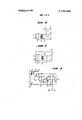
- the reference numerals 9, 10 and 11 given in FIG. 3 indicate the output terminals of the DC power supply means of FIG. 1.
- amanuallyturnable knob 160 is secured with a shaft 161 and'a dial 162 which is marked with an index 163.
- Another dial 164, attached to the camera body, is marked with'an index 165.
- the shaft 161 is coupled with a shaft'167 of housing 166 containing the aforesaid variable resistor 159, so that the resistance of this variable resistor 159 is to be changed by the manual turn of the knob 160.
- a magnet 168 is attached to a yoke 169 of the aforesaid meter 154, and a movable coil 170 is secured with a pointer 171.
- the photoelectric element 62 in the monitoring circuit of FIG. 4 or 9 is turned so as to be radiated directly by the flashtube 23.
- Variable resistor 153, photoconductor 152, power supply 155 and meter 154 combine to make up the mentioned semiautomatic exposure setting mechanism as in the precedingly described embodiment of FIG. 9. Only the changeover switch 156 of FIG. 9 is absent here. For taking pictures by daylight, a proper setting of shutter speed causes a corresponding change in the resistance of the variable resistor 153. Of the T.T.L.
Landscapes
- Physics & Mathematics (AREA)
- General Physics & Mathematics (AREA)
- Stroboscope Apparatuses (AREA)
- Exposure Control For Cameras (AREA)
Abstract
An electronic flash system including a flashtube for producing a controlled quantity of light energy, a plurality of capacitors in which is stored electrical energy to be translated into the light energy in the flashtube and which are to be selectively coupled to the flashtube, a monitoring circuit for generating a signal when the quantity of the light energy produced by the flashtube has reached a predetermined value, bypass means for causing the electrical energy discharged from a capacitor coupled to the flashtube to bypass the flashtube in response to the signal generated by the monitoring circuit, and a control circuit becoming operative when the electrical energy discharged from the capacitor that has been coupled to the flashtube falls short of a desired quantity of light energy to be produced and selectively coupling the rest of the capacitors to the flashtube until the desired quantity of light energy is emitted thereby.
Description
United States Patent [1 Ban ' Filed:
ELECTRONIC FLASH SYSTEM Inventor: ltsuki Ban, Tokyo, Japan I Assignees: Secoh Giken Company Limited;
Miyata Electric Works,'lnc., Tokyo, Japan Dec. 3, 1971 Appl. No.: 204,579
Foreign Application Priority Data 9 Dec. 5, 1970 Japan. 45/107198 U.S. Cl...' 95/10 CE, 95/115 R, 315/241 P Int. Cl. G03b 15/05 Field of Search 95/115 R, 10 CE;
References Cited v UNITED STATES PATENTS 3/1972 Ratsch; 315/241 X 8/1972 Ont) etal 315/241 X 3/1972 Ackermann 95/11.5 X 8/1959 MOSt....L 95/115 X 11/1966 Bramer, 95/115 3/1972 Bisber 95/l1.5
Primary Examiner-Samuel S. Matthews Assistant Examiner-Michael L. Gellner Attorney-Eric 1-1. Waters et a1.
[57] ABSTRACT An electronic flash system including a flashtube for producing a controlled quantity of light energy, a plurality of capacitors in which is stored electrical energy to be translated into the light energy in the flashtube and which are to be selectively coupled to the flashtube, a monitoring circuit for generating a signal when the quantity of the light energy produced by the flashtube has reached a predetermined value, bypass means for causing the electrical energy discharged from alcapacitor coupled to the flashtube to bypass the flashtube in response to the signal generated by the monitoring circuit, and a control circuit becoming operative when the electrical energy discharged from the capacitor that has been coupled to the flashtube falls short of a desired quantity of light energy to be produced and selectively coupling the rest of the capacitors to the flashtube until the desired 'quantity of light energy is emitted thereby. l
17 Claims, 17 Drawing Figures 3,748,989 9 14 1 July 31, 1973 I PATENTEU JUL 3 1 I973 sum 3 or 6 PAIENIEDJULEI 1 ma v 3, 7 9
sum u or 6 m-nmumms 3,748,989
SHEET 5 [IF 6 PATENIEUIJULS 1 ma, 748,989
' sum a nr 6 1 ELECTRONIC FLASH SYSTEM BACKGROUND OF THE INVENTION This invention relates to an electronic flash system for photographic and other applications, and more particularly to an improved electronic flash system capable of automatic control of the quantity of light energy produced by a flashtube provided therein.
According to a conventionally known counterpart of the electronic flash system of the invention, a monitoring circuit is provided which integrates a quantity of light energy produced by a flashtube and which generates a signal when the quantity of light energy has been integrated to a predetermined value, whereupon the electrical energy being discharged from a capacitor coupled to the flashtube is made to bypass the flashtube for the correct exposure of a photographic fllm or the like. Such known electronic flash system has an advantage in that the lens aperture of the camera need not'be calculated for invidual shootings according to a specified Guide Number. I
In order to take photographs of objects or scenes at widely varied distance under automatic control of a quantity of light energy produced each time by a flashuse of the electrical energy stored in the capacitor or capacitors, the energy being wasted as it bypasses the flashtube to terminate, its radiation. It has been confirmed that up to 80 percent of the objects in usual picture-taking situations are located within a distance of about 3 meters from the camera. Accordingly, assuming an average lens f-number of 5.6, a Guide Number of about 16 (in meters) will be enough for the production of thelight quantity" needed for correct exposure in most cases. In-the prior art'electronic flash system'of the kind referredto above,- therefore, asmuchas 75 to 80 per cent of the electrical energy stored in the capacitor or capacitors'is wasted.
Such a large percentage of wasted energy poses a problem not to be overlooked in case dry cells are being used as the power source of thesystem or, for that matter, even in the case of rechargeable power sources such as nickel cadmium batteries, in which latter case flashlight" is obtainable only an unduly small number of times after eachbattery recharging. This number will be multiplied almost four" times under usual conditions if the electrical energy that has been wasted as above is reduced to a minimum.
SUMMARY OF THE INVENTION.
It is accordingly aprimary objectofthepresent invention to provide a new and better electronic" flash system capable of automatically controlling the quantity of light energy produced bya flashtube for theycorrect exposure of a photographic film or the like.
Another object of the invention is to provide an electronic flash system so made that when a quantity of "the light energy produced by'a flashtube has attained a predetennined value, the electrical energy that has been supplied to the flashtube is made to bypassthe' same in' order to terminate its radiation.
Still another object of the invention isto provide an electronic flash system so made that the electrical energy which is wasted as it bypasses a flashtube in order to terminate its radiation is reduced to a minimum.
Yet another object of the invention is to provide an electronic flash system wherein a plurality of capacitors charged with electrical energy to be translated into light energy in a flashtube are selectively or succes sively coupled to the flashtube until a desired quantity of flashlight is radiated by the flashtube, whereupon only the electrical energy being disch'arged'from the capacitor coupled to the flashtube at that moment is made to bypass the same, so that only a minimum quantity of electrical energy is expended for each flash operation.
Yet a further object of the invention'is' to provide ancontrolled for correct exposure of the film loaded in the camera according to its'lens aperture value and distance to an object or scene tojbe photographed.
A further object of the invention is to provide an electronic flash system so made that the duration of its flash impulse is variable according to the specified exposure index of the film being used", so that correct exposure will always result even when film having different exposure indices are used". I
Further objects of the invention, as well as the characteristic features thereof, will be {apparent from the following detailed description, when read with reference to the accompanying drawings showing, by way of example only, several preferred forms of the electronic flash system in accordance with the present invention.
BRIEF DESCRIPTION OF THE DRAWINGS- In' the drawings: FIG. 1 is a circuit diagram. of an example of power supply means for use in the. electronic flash system of the present invention;
FIG. 2 is a circuit diagram of another example of the power supply means;
FIGS. 7(a), (b')..and (.c') are. views explanatory of an exposure calculator dial for use with: the electronic flash system of the" present invention;
FIG. 8 is a. circuit diagram ofstill another preferred embodiment of the present: invention;
FIG. 9 is a circuit diagram showing a monitoring: circuit, forusein the electronic flash system of the invention, with relation to the related mechanisms of'acmaera;
FIG. 10 is a circuit diagram showinganothen example of the relationship between: the: monitoringcircuitandthe related mechanisms of a camera;
DESCRIPTION OF THE PREFERRED EMBODIMENTS FIGS. 1 and 2 of the drawings illustrate two different examples of DC power supply means for use in an electronic flash system of the present invention. Referring now more specificallyto FIG. 1, a power supply 1 is connected to a transistor oscillator circuit 2 via a switch 3. The oscillating output of this transistor oscillator circuit 2 is fed to a transformer 4, where it is raised in voltage, and then fed to a voltage doubling circuit comprised of diodes 5 and 6 and capacitors 7 and 8, where the elevated output voltage of the transformer 4 is rectifiedintodirect voltage having-approximately twice the peak amplitude of the applied voltage. The desired DC power thus produced is obtained at output terminals 9, 10 and 11 of the DCp-ower supply means with the respective polarities indicated in the drawing.
FIG. 2 illustrates another example of the DC power supply means, in which power supply 1 is connected to transistor oscillator circuit 2 via switch 3. The oscillating output of this transistor oscillator circuit 2 is similarly directed to transformer 4, where it is raised in voltage and thence to a diode 12, where the elevated output voltage of the transformer 4 is rectified. Hence the DC output is obtained from output terminals 14 and 15 with the respective polarities indicated. The potential of another output terminal 13 is higher than that of the output terminal .14 by the voltage of the power supply 1.
The two examples of the DC power supply means shown and described in the'foregoing two paragraphs carry the reference numeral 16 in FIGS. 3 and 8 illustrating two different fonns of the electronic flash system in accordance with the present invention.
Referring now to FIG.-3 which illustrates the circuit configuration of an electronic flash system in a first embodiment of the invention, capacitors l7 and 18 serve for the storage of electrical energy to be translated into light energy in the form of flashlight. One of these capacitors 18, is so connected as to be charged via a diode 19 and to be discharged via a silicon controlled rectifier 20 (hereinafter referred to as an SCR.) Upon closure of a switch 21, a gate signal is applied to the gate terminal of this SCR 20 via a resistance 22 as indicated bythe arrow, whereupon conduction takes place therein so that the capacitor 18 is now connected to the circuit for delivering the electrical energy stored therein to a flashtube 23 causing the same to emit a flash of light. As the switch 21 is opened, the SCR 20 returns to the nonconducting state upon completion'of the charging of the capacitor 18 and hence is isolated from the aforesaid delivering circuit. The reference numerals 9, 10 and 11 given in FIG. 3 indicate the output terminals of the DC power supply means of FIG. 1.
In case the DC power supply means of FIG. 2 is used in place of that of FIG. 1 in the electronic flash system of FIG. 3, with the reference numerals 9, '10 and 11 therein substituted with the reference numerals 13, 14 and 15 to designate the output terminals of the former, a voltage obtained from the output terminals 13 and 14 is smaller so that the resistance 22 of FIG. 3 has to be of a correspondingly smaller value.
Further with relation to the electronic flash system of FIG. 3, a circuit incorporating resistances 25 and 26, a capacitor 27, a synchronized switch 28 and a trigger transformer 29 is conventionally well known as that for the application of a trigger pulse to the aforesaid flashtube 23 in the so-called synchrofiash mechanism of a camera. Upon operation of a camera shutter (not shown), the synchronized switch 28 is closed so that the output from the secondary side of the trigger transformer 29 is impressed to a trigger electrode 24 of the flashtube 23 thereby to cause the same to flash. An output terminal 32 is connected to a monitoring circuit still to be described with connection to FIG. 4, for the supply of a voltage thereto via a resistance 30, whereas input terminals 33 and 34 are connected to the output terminals of the monitoring circuit of FIG. 4. Upon application of a pulse to the gate and the cathode of a SCR 31 through these input terminals 33 and 34, respectively, conduction is initiated therein, whereupon the capacitors 17 and 18 are shorted with their electrical energy bypassing the flashtube 23 to extinguish the radiation of the same. Since the shorting current that flows in this instance is considerably large in value, the
' SCR in use has to be of appropriately large capacity. In
view also of the fact that this shorting current is of such short duration, its current rating may be from about 3 to 5 amperes.
FIG. 4 illustrates the circuit configuration of the aforesaid monitoring circuit, whose terminals 35, 36 and 37 are connected to the output terminal 32 and the input terminals 33 and 34, respectively, of the circuit of FIG. 3. This monitoring circuit is comprised of diodes 38 and 39, resistances40,4l, 42, 43, 44, 45, 46, 47, 48, 49, and 51, a variable resistor 52, capacitors 53, 54', 55, 56, 57 and 58, transistors 59, 60 and 61,
It will now be clear that the timing of the extinction of. the flashtube 23 is determinable as desired by varying the resistance of the variable resistor 52, Further 'with reference to the above described monitoring circuit of FIG. 4, the trigger transformer 64 is not neces. sarily an inevitable component, but the surge current produced upon conduction of the SCR 62 may be permitted to flow directly to the gate of the SCR 31. However, in case a quench tube (a low-impedance gasfilled relay tube) is used in place of this SCR 31, the secondary side of the trigger transformer 64 may have to be utilized for the production of high-voltage pulses to be impressed to the trigger electrode of the quench tube thereby to cause the above described bypassing operation of the capacitors 17 and 18. a
How the photoelectric element 63 in the monitorin circuit of FIG. 4 is subjected to radiant energy will now be described with reference'to FIGS. 5(a) and (12). Referring first to FIG. 5(a), the flashtube 23 (given also in FIG. 3) is provided with a reflector 65, thereby to emit the flashlightof the same toward an object or scene to be reproduced in the direction of the arrows B. Light of reduced intensity is to be emitted from a side projection 66 of the reflector '65 through a gray light filter (not shown). The photoelectric element 63 of which the light reflected from the object in the direction of the arrow C impinges upon the photoelectric element 63. As illustrated in greater detail in FIG. 5(b), the casing 67 containing the photoelectric element 63 is pivoted by means of a shaft 70 so as to be revolvable inthe lateral direction by 90 by manually turning a knob 69. Hence, turned 90 in the direction of the arrow D, as indicated in FIG. 5(a), the casing 67 hasits aperture 68 against the side projection 66 of the reflector 65, from which the aforesaid reduced light of the discharge tube 23 radiates the photoelectric element 63. It is accordingly possible to subject the photoelectric element 63 to the direct light of the discharge tube 23 or to the light reflected from the object by a simple turn of the knob 69. i
i As may have been understood from the preceding descriptions made with reference to FIGS. 3 to 5, if the photoelectric element 63 is preadjusted so as to receive the .light reflected from the object, for example, the flashlight of the flashtube 23 emitted in synchronism with-the operation of-the camera shutter as above is ex tinguishedby the shorting of the capacitors 17 and 18 due to the output of the trigger transformer 64 pro.- duced when the photoelectric element 63 is radiated to a predetermined degree. Hence the object can be photographed under proper exposure. What is to be noted here is that the resistance of the variable resistor 52 in the monitoring circuit of FIG. 4 has to be adjusted in accordance with the lens aperture and the film sensitivity. Presumably, the capacitor 17 can have such a capacitance as to provide a Guide Number of 16, or the capacitors 17 and 18 can have such a total capacitance as to provide a Guide Number of 37. Then objects at comparatively short distances (e.g 3 meters) are suf ficiently photographable by use of the Capacitor 17 alone, so that the electrical energy wasted upon con.- duction of the SCR 31 is thus greatly reduced. Underexposure will result, however, when only the energy of the capacitor 17 is used to light the flashtube 23. It is only in such case that the conduction of the SCR 20 in the circuit diagram of FIG. 3 automatically takes place, as mentioned already and described in greater detail hereinbelow with reference to FIG. 8.
Like reference numerals used in FIGS. 3 and 8 indi: cate like ci cuit elements having substantially the same fun so that these elements. in FIG. 8 will not be d scri d ny further- The primary difference resides in a detecting circuit comprised, of resistances 71 and 72, neon-glow tube 73, transistors 74 and 75, and resistances 76 and 77. Proceeding now to the operation of this circuit of FIG. 8 embodying the present invention, the neonvglow tube 73 goes off as the discharge voltage of the capacitor 17 drops close. to the voltage at which the flashtube 23 is extinguished. Since then the primary current of a triggertransformcr 78 is shut off through a resistance 76, the resultant induced vol,
age in the secondary winding of the same causes-a base to initiate its conduction whereupon the capacitor 18 causes the renewed flashing of the flash lamp 23. Hence, following the discharge of the capacitor 17, the other capacitor 18 is automatically discharged as re! quired to increase the total amount of light emitted by the flashtube 23.
It will now be clear that a still greater quantity of light energy is obtainable by the provision of a third capaci tor, complete with another SCR such as SCR 20 provided for the discharge of the capacitor 18 of FIG. 8, in combination with an additional circuit for detecting the drop of the discharge voltageof the capacitor 18 close to the'voltage at which the flashtube 23 is extinguished. If it is difficult to provide three or more such capacitors for the storage of electrical energy in a single electronic flash device, a separate casing may be prepared which contains those capacitors and the aforesaid detecting circuit, with the necessary termi nals led out of the casing for connection with the neces sary parts of the electronic flash unit.
R f rring again to FIG. 8, there occurs an instanta neous flow of charging current from the capacitor 18 to the capacitor 17 upon conduction of the SCR 2.0, so that the SCR 20 will have to be of sufficiently large capacity. But this capacity may be reduced to a desired minimum by the provision of a diode 79 indicated by the dotted lines in the circuit diagram of FIG. 8. As described already, when only the discharge of the capaci tor 17 is required for taking a photograph of an object or scene at closer distances, the monitoring circuit of FIG. 4 supplies its pulses output to the SCR 31 from the input terminals 33 and 34 thereby to initiate its conduction when the photoelectric element 63 provided in j that monitoring circuit has been irradiated to a desired degree. Thereupon the remaining electrical energy of the capacitor 17 bypasses the flashtube 23 for correct exposure. In this instance, however, the capacitor 17 may have its voltage rapidly reduced to such a degree that the neon-glow tube 73 is extinguished, with the result that the SCR 20 becomes conductive to cause the undesired discharge of the other capacitor 18. This defieiency is overcome according to the present invention by the provision of such additional circuit elements as a capacitor 80, SCR 81 and a trigger transformer 82, as indieated'in FIG. 8. Thus the aforesaid pulse output of the monitoring circuit of FIG. 4, introduced from the input terminals 33 and 34, is applied to the trigger transformer 82, so that the resultant pulse output from the secondary winding of the same transformer 82 initiates the conduction of the SCR 81 via the capacitor 80 therebyto prevent the extinction of the neon-glow tube 73 for a short period of time. The flashtube 23 may be caused to complete its flashing due to the discharge of the capacitor 17 within this period of time, thus preventing the succeeding discharge of thecapacitor 18. The capacitor '80 charged as above is discharged by means of a resistance 83 to make itself ready for the ensuing operation.
Alternatively, the same object is attainable as follows: A transformer 82, indicated by the dotted lines in FIG. 8, has its primary side series connected with the SCR 31, to offer extremely low impedance, so that a pulse voltage is induced on the secondary side of this transformer 82 when the bypass current starts to flow upon conduction of the SCR 31. The pulse voltage so induced as utilized as a gate signal of the SCR 81,
thereby to initiate its conduction and hence to prevent the premature extinction'of the neon-glow tube 73.
The neon-glow tube 73 used in the detecting circuit in the embodiment of the invention illustrated in FIG.
8 may be replaced by an avalanche diode without need for the modification of that detecting circuit. Further the SCR 20 may be replaced by a quench tube, in I which case the current flow upon conduction of the transistor 75 is applied to the primary side of the trigger transformer 82, the resultant high-voltage pulse signal induced on the output side thereof being impressed to the trigger electrode of that quenching tube. Furthermore, instead of the quenching tube, another flashtube which may be of the same design as the flashtube 23 may be installed inside the reflector 65 of FIG. 5. By impressing the high-voltage pulse signal induced on the output side of the trigger transformer to the trigger electrode of the second flash tube, the electrical energy of the capacitor 18 is successfully utilized for its flashlight. By such a configuration, illustrated in detail in FIG. 12, the electrical energy to be wasted upon conduction of the SCR 20 (or the quench tube as its substitute) can be translated into radiant energy.
Referring now to FIG. 12 which illustrates the circuit configuration of a further example of the electronic flash system of the invention, the reference character 84 indicates DC power supply means having two output terminals with their respective polarities as indicated in the drawing. The aforesaid second flashtube'85 is assumed to be juxtaposed with the first flahstube 23 within one and the same reflector. Further in this circuit of FIG. 12, a trigger transformer 87, transistors 88 and 89, and resistances 90, 91, 92, 93,94 and-95, etc. are connected as illustrated. A neon-glow tube 96 is kept extinguished as long as electrical energy is stored in the capacitor 17, and is to be lit before the completion of the flashing of the flashtube 23 caused by the discharge of that energy, as explained in greater detail hereinafter. A capacitor 97, which is of large capacitance, is charged via a diode 98, so that its voltage is kept unvaried even when the voltage of the capacitor 17 drops rapidly to supply its discharge to the flashtube 23. As long as the capacitor 17 is charged, the neonglow tube 96 is kept extinguished since the voltage at both ends thereof is less than that needed for its firing. As the voltage of the capacitor 17 drops along with the flashing of the first flashtube 23, the neon-glow tube 96.
lights up owing to the resultant voltage drop of the resistance 94, at a moment preceding the complete extinction of the flashtube 23. A sudden increase in the base is reduced to a minimum. It will accordingly be seen that the electronic flash system in accordance with the present invention is particularly advantageous for taking photographic pictures of. objects or scenes at closer distances.
With reference again to FIG. 12, when only the electrical energy of the capacitor 17 is required, the output signal of the monitoring circuit of FIG. 4, supplied from the input terminals 33 and 34 to the SCR 31 thereby to cause the remaining electrical energy of the capacitor 17 to bypass the first flashtube 23, is also impressed to a trigger transformer 99. The resultant voltage induced in the secondary winding of this trigger transformer 99 initiates the conduction of a SCR 100,.so that the voltage across the neon-glow tube 96 doesnot change to such a degree as to light it up. The flashing of the flashtube 23 is completed in the meantime. The neon tube 96 is'kept extinguished until the capacitor 17 is recharged by the DC power supply means 17, since the resistance 94 does not suffer the aforementioned voltage drop thanks to the voltage of the capacitor 97 supplied via a resistance 101 and theSCR 100. Thereafter, as the resistances 93 and 94 are made again to carry current, the voltage on the cathode side of the SCR 100 rises thereby to automatically switch this SCR 100 to the nonconducting state and hence make it ready for the next operation. Further, the output pulses of the trigger transformer 99 have to'be of such duration that the conducting state of the SCR 100, initiated upon reduction in the current carried by the resistance 94, lasts for a sufficient period of time.
As may be understood from the foregoing, the dis charge of the capacitor 18 does not take place since the detecting circuit including the neon-glow tube 96 is prevented from operating even when the voltage of the capacitor 17 drops further, after its discharge has been made, to bypass the flashtube 23 by the SCR31. While the aforementioned second flashtube may be juxtaposed with the first flashtube 23 so as to make use of one and the same reflector as mentioned above, a circuit including all or part (the flashtube 85 and the capacitor 18 being indispensable) of the flashtube 85, the diode '19, the capacitor 18, the trigger transformer 87 and 99, the SCRs 102 and 100, the capacitors 103, 104 and 97, the resistances 105, 106, 90, 91, 92, 93, 94 and 95, and the transistors 88 and 89 may be provided in a separate casing, with means for connection with the main electronic flash unit, for the convenience of the user.
FIG. 6 illustrates the circuit configuration of still a further example of the electronic flash device of the present invention, in which DC power supply means 84 has positve and negative output terminals like the DC I power supply means used in the precedingly described embodiment of the invention given in FIG. 12. The capacitor 18 in the example of FIG. 6 is provided with a controlled rectifier 46 capable of permitting conduction in both directions (e.g., one known by the trademark Triac), in addition the diode 19 This property of the controlled rectifier 108 makes it possible for the capacitor 18 to be charged and discharged as required. Hence the objects of the present invention are attainable by providing a circuit for the detection of the completion of the discharge of the capacitor 17 as in the previously described embodiment of FIG. 8 and by applying a gate control signal to the controlled rectifier 108 from an appropriate switching circuit. A quench tube 109 is used for the shorting of the capacitors 17 and 18 upon completion of desired flashing. As-in the foregoing embodiments of the invention, the output signal of the monitoring circuit of FIG. 4, to be produced when a desired amount of light has been flahsed bythe flashtube 23, is impressed to a trigger electrode 110 from the input terminals 112 and 113 therebyto cause the discharge of the quench tube 109. The aforementioneddiode 19, provided for the charging of the capacitor 18, maybe dispensed with for reasonsdescribed already. A capacitor 114 of large capacitance is to be charged via a diode 115 so as to serve as a power supply for transistors 116 and 117. Although the capacitor 17 suffers a voltage dropdue to the discharge of the quench tube 109 caused by the supply of the output signal of the'monitoring circuit as above, conduction takes place in SCR 118 by the output voltage of a trigger transformer 119, so that a neon-glow tube 120 is kept lit through a resistance 121. The controlled rectifier 108 thus remains nonconducting, nor is the capacitor 18 discharged. Resistances 122 and 123 again carry current upon completion of the recharging of the oncedischarged capacitor 17, the resultant rise in .the cathode voltage of the SCR 108 switching the same to the nonconducting state thereby to make it ready for the ensuing operation. In the event a desired amount of flashlight is not obtained by the-complete discharge of the capacitor 17, the neon-glow tube 120 is extinguished by the voltage drop at both ends of the resistance 122 prior to the termination of the flashing of the flashtube 23. Accordingly, the value of the current that flows in the transistors 116 and 117 rapidly decreases,
and the trigger transfonner 22 is energized to initiate the conduction of the controlled rectifier 108. Thereupon the electrical energy stored in the other capacitor 18 is discharged to maintain the flashing of the flashtube 23. When the desired amount of flashlight is thus obtained, the quench tube 109 is triggered to the conducting state by the output signal of the monitoring circuit of FIG. 4 so that the remaining electrical energy, if any,'of the capacitor 18 is made to bypass the flashtube 23 thereby to cut short its flashing.
Now, according to thepresent invention, there are two ways of operating the electronic flash system of the invention when the casing 45 of FIG. 5(a) is turned 90' in the direction of the arrow D as indicated in the draw- .ing so that the photoelectric element 163 contained therein is subjectedto the direct radiation of the flashtube 23. The first is to make use of some adequate means for calculating correct exposure, such as for ex-' ample an exposure calculator of FIG. 7, and the other is to operate the electronic flash system of the invention in conjunction with a lens aperture-regulating means and a focusing means of a camera, as illustrated by way of example in FIGS. 9, 10 and 11.
Referring now to FIG. 7 in order to explain the construction and the use of the exposure calculator means illustrated therein, there are to be provided at the back of the electronic flash system casing a knob 125 and a dial 126 which are secured to a shaft 127. This shaft 127 is coupled with a housing 128, as illustrated in FIG. 7(b), which contains the variable resistance 52 of FIG. 4 having a pair of terminals 129. Hence the value of this resistance 52 is to be controllably varied by the manual rotation of the knob 125. There is also secured to the aforesaid shaft 127 a sleeve 130 to which are secured slidersl31 and 132 so as to be slidable upon a switching disk 133. As illustrated in detail in FIG. 7(c), this switching disk 133 is provided with electrically conductive portions 134 and 135, the conductive portion 134 maintaining contact with the slider 132 so as to serve as a slip ring, and the other conductive portion 135 contacting the slider 131 only through an appropriately predetermined angle. A switch is thus composed of the respective terminals 136 and 137 of the conductive portions 134 and 135, to be made only while the knob 125 is turned in the direction of the arrow B through the angle defined by the conductive portion 135. This switch corresponds to switch 21 in FIG. 3. Hence, when the knob 125 is turned within the predetermined angle, the capacitor 17 alone supplies its energy to the flashtube 23, whereas, when the knob is turned in excess of that angle, the other capacitor18 supplies its energy to the same flashtube in order to increase the amount of the flashlight radiated thereby.
With referenceback to FIGS. 7(a) and (b), dials 126 I and 138 are mounted on the shaft l27-so as to be freely turnable independently of each other onthe frame 139.
. The dial .126 is marked with indices 140 and 141,
whereas the other dial 138 is marked with a set of calibrations 142 to indicate lens aperture and with another set of calibrations 143 to indicate distance to an object or scene to be reproduced. The frame 139 is marked with a set of calibrations 144 to indicate film exposure index (in ASA, for example), and with another set of calibrations 145, seen through a slot 146 cut open in the dial 138, to indicate the duration of a flash impulse.
For taking photographs, a lens aperture setting of the camera on the calibrations'l45 is adjusted to the exposure index of thefilm in use on the calibrations 144 by turning the dial 138 by means of va knob 147 attached thereto. The index 140 is set to the visually estimated distance to the object or scene on the calibrations, 143 by turning of the knob 125, so that the aforementioned housing 128 coupled therewith is turned to vary the value of the variable resistance 52 of FIG. '4. Upon shooting, the electrical energy stored in the capacitor 17 is bypassed when the desired'amount of flashlight, prescribedby the variable resistance 52, has been obtained. In case agreater quantity of flashlight is required for correct exposure, the slider 131 comes in contact with the electrically conductive portion since then the dial 126 is turned-farther in the direction of the arrow E of FIG. 7(c), so that the resultant closure of the switch 21 of FIG. 3 causes-the other capaci- 'tor 18 to supply its electrical energy for the radiation of the greater quantity of flashlight required. Needless to say, the value of the variable resistance 52 is varied correspondingly. The index is to meet the index 148 to indicate a point where the other capacitor 18 is to take part in the radiation of flashlight, thereby enabling the photographer to make use of only the electrical energy stored in the capacitor 17 through proper setting of lens aperture. In contrast with conventional Guide Number calculation, in which case the camera lens aperture has had to be reset for each shooting, the present invention enables obtaining correct exposure only by turning the knob 125 while the lens aperture setting is left unvaried.
Further, according to this invention, the duration of each flash impulse can be determined as desired for taking a photograph of an object moving at extremely high speed or for special photographic effects. Since the variation of the value of the variable resistance 52 of FIG. 3 not only results in the variation of the quantity of flashlight radiated but in the duration of the flash impulse, the knob 125 of FIG. 7(a) or (c) is turned to adjust the value of desired flash impulse duration on the calibrations 145 with the index 141. The other knob 147, attached to the dial 138, is turned to adjust a value of estimated distance to the object on the calibrations 143 with the other index 140. A lens aperture value corresponding to the exposure index of the film in use is read from the calibrations 142 to set the lens aperture of the camera to that value. It is thus possible to take a photograph under correct exposure and in the prescribed flash impulse duration. This duration may be varied within therange of from l/50,000 to l/l000 second.
Needless to say, the positions of the calibrations 744 and the calibrations 142 as well as the positions of the index 140 and the index 143 are freely interchangeable. It will also be obvious that, when the exposure calculator means of FIG. 7 is used in combination with the circuit of FIG. 8, the switch mechanism (corresponding the lens aperture-regulating mechanism and the focus ing mechanism of the camera. In this figure, terminals 35, 36 and 37 are respectively connected to the output terminal 32 and the-input terminals '33 and 34 of the to the switch 21 of FIG. 3) comprising the switching disk 133 and the sliders 131 and 132 that are provided on the housing 128 can be'dispensed with. In this case, the capacitor 18 may be made automatically to deliver its energy for the 7 radiation of a greater quantity of flashlight, whenever desired, as the knob 125 is turned in the direction of the arrow E through an increased angle. Furthermore the knob 125 need not necessarily be associated with the variable resistance 52 of FIG. 4. Since the energy of the light radiated by the flashtube 23 can be considered as being proportional to the energy of the input to that flashtube 23, an additional circuit may be provided which is capable of integrating the product of the voltage impressed to the flashtube 23 and the current flowing therein, instead of the photoelectric element 63 which integrates the quantity of the radiated light. A signal to be produced when the result of the integration reaches a predetermined value may be utilized to energize the SCR 31 to the conducting state and'hence to cause the flashtube 23 to terminate its radiation. In this instance, to realize the above explained object of the invention, an integrating capacitor to produce the mentioned signal has to be provided with a variable resistor, which may be coupled to the knob 125 of FIG. 7, thereby to regulate that integrating capacitor.
Reference will now be made to FIG. 9 in order to describe the operation of the electronic flash system of the invention with reference to a camera. FIG. 9 is illustrated to show the interrelation between the monitoring circuit in accordance with the present invention and circuits of FIGS. 8 and 12. The monitoring circuit illustrated here is the same as that of FIG. 4, except that the variable resistor 52 in the monitoring circuit of FIG. 4 is not provided and that a pair of terminals 149 are led out for connection with a pair of terminals 150 of the camera via detachable leads 151. The photoelectric element 63 in the monitoring circuit of FIG. 9 is so positioned as to receive the direct flashlight of the flashtube 23. A photoconductor 152, a variable resistor 153 coupled to a shutter speed dial (not shown), a meter 154 and a power-supply 155 combine to make up thewellknown semiautomatic daylight exposure setting mechanism used widely in single-lens reflex cameras. A
proper setting of camera shutter speed on the shutter speed dial causes the resistance of the variable resistor 153 to be varied correspondingly. The camera lens aperture is then set properly. In a thrdugh-the-lens ('I'TL) type, the light that has passed through the camera lens is received by the photoconductor 152, so that the pointerof the meter 154 deflects in response to change in the camera lens aperture. For correct exposure, the shutter button may be depressed at the moment when the pointer of the meter 154 deflects to a predetermined position. In case the exposure index of the film in use is to be taken into account, the meter l54'to- 'gether with its pointer has to be turned (as indicated by the arrow G) to a calibration corresponding to the exposure index of the film. For taking photographs with use of the electronic flash system of the invention, the camera shutter speed is to be set properly, for example to l/ second in the caseof a focal plane shutter. A
ated to adjust the focus of the camera lens to the object or scene to be photographed, whereupon the resistance of a variable resistor 157 coupled to'the focusing mechanism is changed correspondingly. The lens apertureregulating mechanism is operated for proper setting of the camera lens aperture, thereby causing the resistance of a variable resistor 158 coupled therewith to be changed correspondingly.
Upon shooting, the flashtube 23 of FIG. 8 or 12 rad iates its controlled flashlight for correct exposure. Explained in greater detail, since the sum of the resistance of the variable resistors 157 and 158 corresponds to the resistance of the variable resistor 52 in the monitoring circuit of FIG. 4, this sum determines the duration of the flashlight radiated by the flashtube 23. The variable resistors 157 and 158 are coupled to the focusing mechanism and the lens aperture-regulating mechanism, respectively, in such a manner that the more distant the object or scene to be. reproduced, and the 7 smaller the lens aperture, the smaller are the resistames of resistors 157 and 158. When the sum of the resistances of the variable resistors 157 and 158 is-rendered smaller than a predetermined value, the capacitor l8 automatically delivers its electrical energy to the flashtube 23 in order to increase the total quantity of the light energy radiated thereby.
For taking into account the exposure index of the film in the above embodiment of the invention, the relative locations of the variable resistors 157 and the fo-: cusing mechanism, or the relative locations of the variable resistor 158 and the lens aperture-regulating mechanism, may be changedaccording to the specified value of the film exposure index. The pointer of the meter 154, seen in the camera finder, moves in accordance with the sum of the resistances of the variable resistors 157 and 158. An index may be predisposed at such a position within the finder that pointer deflection in excess of that index indicates that the flashlight radiated by the discharge of the electrical energy from both of the capacitors 17 and 18 will still result in underexposure. In this case the shooting of the subject has to be discouraged. An additional index may be predisposed at another position so that pointer deflection in excess of this additional index is an indication that, upon shooting, the capacitor 18 will deliver its energy to the flashtube 23 to increase the total quantity of the light energy radiated thereby. In this instance, the lens aperture, of the camera may be made largerto reduce the pointer deflection into the range defined by the additional index and hence to make use of the electrical energy stored in the capacitor 17 alone as far as practical. While in'the embodiment of FIG. 9 the photoelectric element 63 is used in the monitoring circuit for integrating the light energy radiated, there may, of
course, be contemplated an alternative arrangement in which the electrical energy supplied to the flashtube 23 of FIG. 8 or 12 is integratedin order to switch the SCR 31 to the conducting state by a signal to be-produced at the moment when the result of the integration reaches a predetermined value, thereby terminating the flashing of the flashtube 23.
FIG. illustrates another example of the interrelation between the electronic flash system of the invention and the camera. In the drawing, a pair of terminals 149 are assumed to be led out of a monitoring circuit of the same configuration as that of FIG. 9, for connection with another pair of terminals 150 led out of the camera by means of leads 151. Theterminals 150 are connected with a variable resistor 159 which regulates the quantity of light energy radiated by the flashtube of the electronic flash system, thus serving the function of the variable resistor 52 of FIG. 4. Variable resistor 153, photoconductor 152, changeover switch 156, power source 155 and meter 154 operate the same way as the respective circuit elements of FIG. 9 carrying the same reference numerals. The functions of the variable resistors 157 and 158 are also the same as the functions of the variable resistors 157 and 158 of FIG. 9. What distinguishes the embodimentof FIG. 10 is the construction of the meter 154 and the variable resistor 159.
Referring now to FIG. 11 in order to describe the meter 154'and the variable resistor 159 in greater detail, amanuallyturnable knob 160 is secured with a shaft 161 and'a dial 162 which is marked with an index 163. Another dial 164, attached to the camera body, is marked with'an index 165. The shaft 161 is coupled with a shaft'167 of housing 166 containing the aforesaid variable resistor 159, so that the resistance of this variable resistor 159 is to be changed by the manual turn of the knob 160. A magnet 168 is attached to a yoke 169 of the aforesaid meter 154, and a movable coil 170 is secured with a pointer 171. A shaft 172 mounted in the camera body turnably supports a secondary pointer 173, which is'to be moved by manually turning of the knob so as to agree. in position with the pointer 170. A member 174 is marked with an index 175. A pointer 176 is secured to the aforesaid yoke 169 of the meter 154. By turning this pointer 176 in the direction of the arrow Gin FIG. 11 by means of a knob or the like (not shown in the drawing), the meter 154 turns together the pointer 171. Hence the pointer 176 is adjustable on calibrations 177 according to the exposure index of the film being used.
To explain the manner of use of. the above described means illustrated in FIGS. 10 and 11, the pointer 176 is firstly adjusted to that position on the set of calibrations 177 corresponding to the exposure index of the film in use. The changeover switch 156 of FIG. 10 is turned to the position indicated by the dots inthe drawing. The focusing mechanism is then operated to focus the camera lens on the object or scene to be reproduced, thereby to change the resistance of the variable resistor 157 correspondingly. The lens aperture is set properly, thereby correspondingly changing the resistance of the variable resistor 158 and also causing the pointer171 of the meter 154 to deflect correspondingly. The knob 160 is turned to adjust the secondary pointer 173 at the previously determined position of the pointer 171, the resistance of the -variable resistor 159 of FIG. 10 being changed correspondingly. Now, upon shooting, the light impulse is radiated whose duration is determined by the resistance of the variable resistor 159 so as to provide a quantity of light energy necessary for correct exposure of the film. The indices 163 and marked on the dials-162 and 164, respectively, may be utilized in such a manner that, as the index 163 comes to agree with the index 165 by turning of the knob 160 to adjust the secondary pointer 173 at the position of the pointer 171 as above, the capacitor 18 is connected in the circuit for delivering the electrical energy stored therein to the flashtube upon shooting. This serves for the economical use of the energy stored in the capacitor 18, as in the precedingly described embodiment of the present invention. The same object is attainable by the index marked on the member 174, in which case the pointer 171 agrees with that index 175 to indicate a point where the capacitor 18 is connected to the aforesaid delivering circuit upon shooting. It is to be understood that the above described procedure of the operations of the focusing mechanism, the lens aperture regulating mechanism, and the knob 160 is purely by way of example.
FIGS. 13(a) and 13(b) are given to explain the relationship between the electronic flash system' of the invention and the related mechanisms of a camera, as well as the construction of variable resistors associated with the lens aperture regulating mechanism and focusing mechanism of the camera. The pair of terminals 149 in FIG. 13 (a) are assumed toQbe led out of the monitoring circuit given in FIG. 9 and are connected through leads 151 with the pair of terminals 150 of the camera. The terminals 150 are provided with a variable resistor 178 which serves the function ,of the variable resistor 52 of FIG. 4, the resistance of this variable resistor 178 being changed to cause a corresponding change in the quantity of light energy to be produced by the electronic flash system of the invention. It is also assumed that in this particular embodiment of the invention, the photoelectric element 62 in the monitoring circuit of FIG. 4 or 9 is turned so as to be radiated directly by the flashtube 23. Variable resistor 153, photoconductor 152, power supply 155 and meter 154 combine to make up the mentioned semiautomatic exposure setting mechanism as in the precedingly described embodiment of FIG. 9. Only the changeover switch 156 of FIG. 9 is absent here. For taking pictures by daylight, a proper setting of shutter speed causes a corresponding change in the resistance of the variable resistor 153. Of the T.T.L. system, the beam of light that has passed through the camera lens aperture regulated by its diagram is received by the photoconductor 152, so that correct exposure will result upon shooting when the pointer of the meter 154 deflects to a prescribed position (to be marked appropriately) by operating the lens aperture regulating mechanism. The pointer of the cated by the dotted lines in the drawing). A ring 181 is manually turnableto move the whole lens system or only the front lens element back and forth for a focusing operation, being turned in the direction of the arrow M for an object at closer distance. The distance to the object is calibrated on 182. Electrically resistive member 178 is pasted or otherwise attached to a portion 183 integral with the ring 181. Electrically conductive member 184 is in contact with the ring 181 and is grounded to the lens housing 179. A ring 185 as a part of the lens aperture regulating mechanism is to be turned clockwise (indicated by the arrow N in the drawing) for increasing the lens aperture, and vice versa. A slider 186 is secured to this ring 185 so as to slide on the resistive member 178 while being in contact at the other end with an electrically conductive portion 187 provided on the right hand side 188 of the lens housing 179 and connected to a contact 190 of a housing end 189 through a lead 191. The end 189 of the lens housing is to be screwed, bayoneted or otherwise secured to the camera body.
The contact 190 of the housing end 189 so secured to the camera body is to be connected with a corresponding contact of the camera body, and the electrically conductive member 184 is to be connected to the camera body itself. By connecting the pair of terminals 150 of FIG. 13 (a),with the grounding terminal of the camera body and its contact connected with the aforesaid contact 190, the resistive member 178 of FIG. 13 (b) serves as the variable resistor 178 of FIG. 13 (a). It will now'be clear that the resistance of this variable resistor 178 is changed by rotating the ring 181 of the in f-number. For this reason, the calibrations 192 have to be marked in lens f-number and to be at equal spacings, and the calibrations 182 also have to be spaced equal to the spacings of thecalibrations 192. Moreover, successive calibrations 182 which indicate the distance to the object have to carry values whose squares are substantially in geometric progression with a ratio of 2. For this purpose, the ring 181 and the lens the relative locations of the ring 185 and the lens aperture regulating mechanism may be varied in an adequate manner according to the specified value of the exposure index. When the object is located at a closer distance and, therefore, when a greater lens aperture is required, the rings 181 and 185 are turned in the directions of the arrows M and N, respectively, so that the resistance of the variable resistor 178 is increased. It
will also be clear that when the resistance of this resistor 178 is rendered smaller than a predetermined value, the capacitor 18 is automatically connected in the aforementioned delivering circuit for correct exposure upon shooting. 1
The contact 190 at the end of the lens housing of FIG. 13 (a) may be dispensed with if the terminal connected with the lead 151 is to be provided directly on the lens housing 179. There may, of course, be contemplated the provision of adequate counterparts of the variable resistor 178 and its terminal 150 to the housings of spare lens systems, if any, to be used in substitution for the lens system 180 of FIG. 13 (b). Further, it is assumed that the variable resistor 178 is such that its resistance increases twice as much each time the ring is turned in the direction of the arrow N by one calibration, although such geometric progression of the resistance of the variableresistor 178 has to be modified according to the construction of the monitoring circuit of FIG. 4 to be used incombination.
Although the electronic flash system of the present invention has been shown and describedin the foregoing in some specific aspects thereof, it is understood that the invention is not to be restricted thereby but includes obvious and reasonable equivalents within the skill of the specialists.
What is claimed is:
1. An electronic flash system comprising, in combination, a flashtube, a plurality of capacitors in which is stored electrical energy to be translated into light energy by means of said flashtube said plurality of capacitors including a first capacitor having a value capable of storing sufficient energy for illumination of said flashtube under conditions of relatively'low level lighting requirements and at least one second capacitor for providing further energy under conditions of higher level lighting requirements when the energy supplied by the first capacitor is insufficient, a circuit for delivering the electrical energy stored in said capacitors selectively to said flashtube, a circuit for monitoring a quantity of the light energy produced by said flashtube,
said monitoring circuit generating a signal at the instant when the quantity of the light energy has reached a predetermined value, bypass means coupled to said monitoring circuit for causing the electrical energy discharged from the capacitor coupled to said delivering circuit to bypass said flashtube in response to the signal generated by said monitoring circuit, the remaining capacitors remaining energized, a detecting circuit for generating a signal when the electrical energy of the capacitor coupled to said delivering circuit has been discharged through said flashtube, and a, control circuit responsive to'the signal generated by said detecting circuit for selectively and successively coupling the rest of said capacitors to said delivering circuit only when the electrical energy discharged from the capacitor which has beencoupled to said delivering circuit is insufficient for said flashtube to produce a desired quantity of light energy.
2. An electronic flash system as claimed in claim 1 wherein said plurality of capacitors consist of a first capacitor always coupled to said delivering circuit and a second capacitor to be coupled selectively to said delivering circuit by means of said control circuit.
3. An electronic flash system as claimed in claim 2 wherein said control circuit includes a solid state de vice coupled between said second capacitor and said delivering circuit for the control of the flowiof current from said capacitor to said flashtube.
4. An electronic flash system as claimed in claim 3 wherein said solid state device is a silicon controlled rectifier.
5..An electronic flash system as claimed in claim 4 wherein said detecting circuit comprises a neon-glow tube which remains conductive until the'electric potential of said delivering circuit drops to a predetermined value, and at least one switching element responsive to the termination of the conduction of said neon-glow tube to initiate conduction in said silicon controlled rectifier. I
6. An electronic flash system as claimed in claim 5 wherein said switching element is a transistor.
7. An electronic flash systemas claimed in claim 4 wherein said detecting circuit comprises a neon-glow tube whose conduction is initiated when the electric potential of said delivering circuit has dropped to a predetermined value, and at least one switching element being responsive to the initiation of the conduction of said neon-glow tube to switch said silicon controlled rectifier to the conducting state.
8. An electronic flash system as claimed in claim 7 wherein said switching element is a transistor.
9; An electronic flash system as claimed in claim 3 ducting state by the signal generated by said monitoring circuit.
12. An electronic flash system as claimed in claiml wherein said monitoring circuit comprises a photoelectric element to be irradiated by said flashtube, an integrating capacitor to be charged with electrical energy in accordance with the quantity of light energy incident on said photoelectric element, a switching element to be switched to the conducting state when said integrating capacitor has been charged with a predetermined quantity of electrical energy, and an adjusting device for varying the moment at which said switching-element is switched, said monitoring circuit generating said signal when said switching element has been switched.
13. An electronic flash system as claimed in claim 12 wherein said adjusting device is a variable resistor whose resistance is manually changeable.
14. An electronic flash system as claimed in claim 12 wherein said adjusting device is a variable resistor whose resistance is changed by operating a focusing mechanism and a lens aperture regulating mechanism -of a camera used in combination with said electronic flash system.
15. An electronic flash system as claimed in claim 14, further comprising means for changing the resistance of said variable resistor according to the exposure index of the film loaded in the camera.
16. An electronic flash system as claimed in claim 12 wherein said adjustingdevice includes a first variable resistor and a second variable resistor which are interconnected. in series, the resistance of said first variable resistor being changed by operating the focusing mechanism of the camera, and the resistance of said second variable resistor being changed by operating its lens aperture regulating mechanism.
17 An electronic flash system as claimed in claim 16, further comprising means for changing the resistance of at least one of said first and said second variable resistors in accordance with an exposure index of the film loaded in the camera.
Claims (17)
1. An electronic flash system comprising, in combination, a flashtube, a plurality of capacitors in which is stored electrical energy to be translated into light energy by means of said flashtube said plurality of capacitors including a first capacitor having a value capable of storing sufficient energy for illumination of said flashtube under conditions of relatively low level lighting requirements and at least one second capacitor for providing further energy under conditions of higher level lighting requirements when the energy supplied by the first capacitor is insufficient, a circuit for delivering the electrical energy stored in said capacitors selectively to said flashtube, a circuit for monitoring a quantity of the light energy produced by said flashtube, said monitoring circuit generating a signal at the instant when the quantity of the light energy has reached a predetermined value, bypass means coupled to said monitoring circuit for causing the electrical energy discharged from the capacitor coupled to said delivering circuit to bypass said flashtube in response to the signal generated by said monitoring circuit, the remaining capacitors remaining energized, a detecting circuit for generating a signal when the electrical energy of the capacitor coupled to said delivering circuit has been discharged through said flashtube, and a control circuit responsive to the signal generated by said detecting circuit for selectively and successively coupling the rest of said capacitors to said delivering circuit only when the electrical energy discharged from the capacitor which has been coupled to said delivering circuit is insufficient for said flashtube to produce a desired quantity of light energy.
2. An electronic flash system as claimed in claim 1 wherein said plurality of capacitors consist of a first capacitor always coupled to said delivering circuit and a second capacitor to be coupled selectively to said delivering circuit by means of said control circuit.
3. An electronic flash system as claimed in claim 2 wherein said contRol circuit includes a solid state device coupled between said second capacitor and said delivering circuit for the control of the flow of current from said capacitor to said flashtube.
4. An electronic flash system as claimed in claim 3 wherein said solid state device is a silicon controlled rectifier.
5. An electronic flash system as claimed in claim 4 wherein said detecting circuit comprises a neon-glow tube which remains conductive until the electric potential of said delivering circuit drops to a predetermined value, and at least one switching element responsive to the termination of the conduction of said neon-glow tube to initiate conduction in said silicon controlled rectifier.
6. An electronic flash system as claimed in claim 5 wherein said switching element is a transistor.
7. An electronic flash system as claimed in claim 4 wherein said detecting circuit comprises a neon-glow tube whose conduction is initiated when the electric potential of said delivering circuit has dropped to a predetermined value, and at least one switching element being responsive to the initiation of the conduction of said neon-glow tube to switch said silicon controlled rectifier to the conducting state.
8. An electronic flash system as claimed in claim 7 wherein said switching element is a transistor.
9. An electronic flash system as claimed in claim 3 wherein said solid state device is a Triac.
10. An electronic flash system as claimed in claim 9 wherein said bypass means includes a gas-filled relay tube connected in parallel with said flashtube, said gas-filled relay tube becoming conductive in response to the signal generated by said monitoring circuit.
11. An electronic flash system as claimed in claim 2 wherein said bypass means includes a silicon controlled rectifier connected in parallel with said flashtube, said silicon controlled rectifier being switched to the conducting state by the signal generated by said monitoring circuit.
12. An electronic flash system as claimed in claim 1 wherein said monitoring circuit comprises a photoelectric element to be irradiated by said flashtube, an integrating capacitor to be charged with electrical energy in accordance with the quantity of light energy incident on said photoelectric element, a switching element to be switched to the conducting state when said integrating capacitor has been charged with a predetermined quantity of electrical energy, and an adjusting device for varying the moment at which said switching element is switched, said monitoring circuit generating said signal when said switching element has been switched.
13. An electronic flash system as claimed in claim 12 wherein said adjusting device is a variable resistor whose resistance is manually changeable.
14. An electronic flash system as claimed in claim 12 wherein said adjusting device is a variable resistor whose resistance is changed by operating a focusing mechanism and a lens aperture regulating mechanism of a camera used in combination with said electronic flash system.
15. An electronic flash system as claimed in claim 14, further comprising means for changing the resistance of said variable resistor according to the exposure index of the film loaded in the camera.
16. An electronic flash system as claimed in claim 12 wherein said adjusting device includes a first variable resistor and a second variable resistor which are interconnected in series, the resistance of said first variable resistor being changed by operating the focusing mechanism of the camera, and the resistance of said second variable resistor being changed by operating its lens aperture regulating mechanism.
17. An electronic flash system as claimed in claim 16, further comprising means for changing the resistance of at least one of said first and said second variable resistors in accordance with an exposure index of the film loaded in the camera.
Applications Claiming Priority (1)
| Application Number | Priority Date | Filing Date | Title |
|---|---|---|---|
| JP45107198A JPS4817334B1 (en) | 1970-12-05 | 1970-12-05 |
Publications (1)
| Publication Number | Publication Date |
|---|---|
| US3748989A true US3748989A (en) | 1973-07-31 |
Family
ID=14452952
Family Applications (1)
| Application Number | Title | Priority Date | Filing Date |
|---|---|---|---|
| US00204579A Expired - Lifetime US3748989A (en) | 1970-12-05 | 1971-12-03 | Electronic flash system |
Country Status (2)
| Country | Link |
|---|---|
| US (1) | US3748989A (en) |
| JP (1) | JPS4817334B1 (en) |
Cited By (4)
| Publication number | Priority date | Publication date | Assignee | Title |
|---|---|---|---|---|
| US4021824A (en) * | 1974-06-07 | 1977-05-03 | Canon Kabushiki Kaisha | Flash light photographic system for camera |
| US4105929A (en) * | 1976-06-30 | 1978-08-08 | Gte Sylvania Incorporated | Shunt triggered flashtube having safety feature |
| US4192597A (en) * | 1978-10-27 | 1980-03-11 | Polaroid Corporation | Photographic apparatus for selectively actuating a pulsable electronic strobe |
| US5264895A (en) * | 1991-08-23 | 1993-11-23 | Konica Corporation | Flash lighting circuit |
-
1970
- 1970-12-05 JP JP45107198A patent/JPS4817334B1/ja active Pending
-
1971
- 1971-12-03 US US00204579A patent/US3748989A/en not_active Expired - Lifetime
Cited By (4)
| Publication number | Priority date | Publication date | Assignee | Title |
|---|---|---|---|---|
| US4021824A (en) * | 1974-06-07 | 1977-05-03 | Canon Kabushiki Kaisha | Flash light photographic system for camera |
| US4105929A (en) * | 1976-06-30 | 1978-08-08 | Gte Sylvania Incorporated | Shunt triggered flashtube having safety feature |
| US4192597A (en) * | 1978-10-27 | 1980-03-11 | Polaroid Corporation | Photographic apparatus for selectively actuating a pulsable electronic strobe |
| US5264895A (en) * | 1991-08-23 | 1993-11-23 | Konica Corporation | Flash lighting circuit |
Also Published As
| Publication number | Publication date |
|---|---|
| JPS4817334B1 (en) | 1973-05-29 |
Similar Documents
| Publication | Publication Date | Title |
|---|---|---|
| US3568582A (en) | Electronic shutter | |
| US3953864A (en) | Camera device having a photographic flash device combined therewith | |
| US4357087A (en) | Camera incorporated with a movable flash light device | |
| US3971049A (en) | System for recording on the film of a camera data relating to the scene being photographed | |
| US3714872A (en) | Photographic flash exposure control system | |
| US3779142A (en) | Automatic electronic flash device | |
| US4086582A (en) | Exposure control device for a camera | |
| US4047194A (en) | Camera system with means for automatically switching to flash operation | |
| US4005444A (en) | Exposure control system for flash photography | |
| US3638543A (en) | Automatic exposure system for photographic camera | |
| US3823411A (en) | Flash disabling interlock responsive to interchangeable lens selection | |
| GB2071455A (en) | Rangefinder for use with photographic apparatus | |
| US3792484A (en) | Automatic flash control device | |
| US3842428A (en) | Camera flash controls with internal light detection | |
| US4023188A (en) | Electronic flash device for a camera | |
| US3748989A (en) | Electronic flash system | |
| US4360764A (en) | Flash unit having plural flashlamps | |
| US4710012A (en) | Flash photography system | |
| US3610122A (en) | Shutter timing system | |
| JPS6254235A (en) | Electronic exposure adjustment controller | |
| US3779141A (en) | Apparatus for controlling an electronic flash | |
| US3995286A (en) | Electronic strobe with optionally-operable controls | |
| US3626827A (en) | Automatic exposure adjustment device for flash photography | |
| US3633476A (en) | Autoflash switching device for camera | |
| US3344724A (en) | Flash circuit for photographic cameras |