US3731311A - Polyphase encoding-decoding system - Google Patents
Polyphase encoding-decoding system Download PDFInfo
- Publication number
- US3731311A US3731311A US00073470A US3731311DA US3731311A US 3731311 A US3731311 A US 3731311A US 00073470 A US00073470 A US 00073470A US 3731311D A US3731311D A US 3731311DA US 3731311 A US3731311 A US 3731311A
- Authority
- US
- United States
- Prior art keywords
- signal
- signals
- sub
- accumulation
- phase
- Prior art date
- Legal status (The legal status is an assumption and is not a legal conclusion. Google has not performed a legal analysis and makes no representation as to the accuracy of the status listed.)
- Expired - Lifetime
Links
- 238000009825 accumulation Methods 0.000 claims abstract description 53
- 238000012545 processing Methods 0.000 claims abstract description 44
- 230000006835 compression Effects 0.000 claims abstract description 12
- 238000007906 compression Methods 0.000 claims abstract description 12
- 230000009977 dual effect Effects 0.000 claims abstract description 5
- 230000006870 function Effects 0.000 claims description 20
- 230000008878 coupling Effects 0.000 claims description 16
- 238000010168 coupling process Methods 0.000 claims description 16
- 238000005859 coupling reaction Methods 0.000 claims description 16
- 238000000034 method Methods 0.000 claims description 15
- 230000004044 response Effects 0.000 claims description 6
- 238000012217 deletion Methods 0.000 claims 1
- 230000037430 deletion Effects 0.000 claims 1
- 230000010363 phase shift Effects 0.000 description 23
- 239000002131 composite material Substances 0.000 description 17
- 230000000875 corresponding effect Effects 0.000 description 12
- 238000010586 diagram Methods 0.000 description 9
- 230000005540 biological transmission Effects 0.000 description 7
- 239000000872 buffer Substances 0.000 description 7
- 238000005314 correlation function Methods 0.000 description 6
- 239000011159 matrix material Substances 0.000 description 5
- 230000008569 process Effects 0.000 description 4
- 230000009467 reduction Effects 0.000 description 4
- 238000005070 sampling Methods 0.000 description 4
- 230000035508 accumulation Effects 0.000 description 3
- 230000001276 controlling effect Effects 0.000 description 3
- 238000013507 mapping Methods 0.000 description 3
- 230000002238 attenuated effect Effects 0.000 description 2
- 230000008901 benefit Effects 0.000 description 2
- 230000002596 correlated effect Effects 0.000 description 2
- 230000000694 effects Effects 0.000 description 2
- 238000010348 incorporation Methods 0.000 description 2
- WABPQHHGFIMREM-AHCXROLUSA-N lead-203 Chemical compound [203Pb] WABPQHHGFIMREM-AHCXROLUSA-N 0.000 description 2
- 241000791900 Selene vomer Species 0.000 description 1
- 238000013459 approach Methods 0.000 description 1
- 230000000295 complement effect Effects 0.000 description 1
- 230000007423 decrease Effects 0.000 description 1
- 238000013461 design Methods 0.000 description 1
- 238000011161 development Methods 0.000 description 1
- 230000004069 differentiation Effects 0.000 description 1
- 230000001747 exhibiting effect Effects 0.000 description 1
- 238000001914 filtration Methods 0.000 description 1
- 150000002500 ions Chemical class 0.000 description 1
- WABPQHHGFIMREM-VENIDDJXSA-N lead-201 Chemical compound [201Pb] WABPQHHGFIMREM-VENIDDJXSA-N 0.000 description 1
- WABPQHHGFIMREM-NJFSPNSNSA-N lead-209 Chemical compound [209Pb] WABPQHHGFIMREM-NJFSPNSNSA-N 0.000 description 1
- 230000008520 organization Effects 0.000 description 1
- 230000002250 progressing effect Effects 0.000 description 1
- 230000005855 radiation Effects 0.000 description 1
- 230000003252 repetitive effect Effects 0.000 description 1
- 238000007493 shaping process Methods 0.000 description 1
- 230000003595 spectral effect Effects 0.000 description 1
- 238000012800 visualization Methods 0.000 description 1
Images


Classifications
-
- H—ELECTRICITY
- H04—ELECTRIC COMMUNICATION TECHNIQUE
- H04L—TRANSMISSION OF DIGITAL INFORMATION, e.g. TELEGRAPHIC COMMUNICATION
- H04L27/00—Modulated-carrier systems
- H04L27/18—Phase-modulated carrier systems, i.e. using phase-shift keying
- H04L27/22—Demodulator circuits; Receiver circuits
- H04L27/233—Demodulator circuits; Receiver circuits using non-coherent demodulation
- H04L27/2335—Demodulator circuits; Receiver circuits using non-coherent demodulation using temporal properties of the received signal
- H04L27/2337—Demodulator circuits; Receiver circuits using non-coherent demodulation using temporal properties of the received signal using digital techniques to measure the time between zero-crossings
-
- G—PHYSICS
- G01—MEASURING; TESTING
- G01S—RADIO DIRECTION-FINDING; RADIO NAVIGATION; DETERMINING DISTANCE OR VELOCITY BY USE OF RADIO WAVES; LOCATING OR PRESENCE-DETECTING BY USE OF THE REFLECTION OR RERADIATION OF RADIO WAVES; ANALOGOUS ARRANGEMENTS USING OTHER WAVES
- G01S13/00—Systems using the reflection or reradiation of radio waves, e.g. radar systems; Analogous systems using reflection or reradiation of waves whose nature or wavelength is irrelevant or unspecified
- G01S13/02—Systems using reflection of radio waves, e.g. primary radar systems; Analogous systems
- G01S13/06—Systems determining position data of a target
- G01S13/08—Systems for measuring distance only
- G01S13/10—Systems for measuring distance only using transmission of interrupted, pulse modulated waves
- G01S13/26—Systems for measuring distance only using transmission of interrupted, pulse modulated waves wherein the transmitted pulses use a frequency- or phase-modulated carrier wave
- G01S13/28—Systems for measuring distance only using transmission of interrupted, pulse modulated waves wherein the transmitted pulses use a frequency- or phase-modulated carrier wave with time compression of received pulses
- G01S13/284—Systems for measuring distance only using transmission of interrupted, pulse modulated waves wherein the transmitted pulses use a frequency- or phase-modulated carrier wave with time compression of received pulses using coded pulses
- G01S13/288—Systems for measuring distance only using transmission of interrupted, pulse modulated waves wherein the transmitted pulses use a frequency- or phase-modulated carrier wave with time compression of received pulses using coded pulses phase modulated
-
- H—ELECTRICITY
- H04—ELECTRIC COMMUNICATION TECHNIQUE
- H04L—TRANSMISSION OF DIGITAL INFORMATION, e.g. TELEGRAPHIC COMMUNICATION
- H04L27/00—Modulated-carrier systems
- H04L27/18—Phase-modulated carrier systems, i.e. using phase-shift keying
- H04L27/22—Demodulator circuits; Receiver circuits
- H04L27/233—Demodulator circuits; Receiver circuits using non-coherent demodulation
- H04L27/2332—Demodulator circuits; Receiver circuits using non-coherent demodulation using a non-coherent carrier
Definitions
- This invention relates generally to encoding and decoding systems and more particularly to an improved digital system of reduced complexity and increased accuracy for decoding and amplitude weighting sequences of polyphase encoded signals.
- a recently developed digital polyphase decoding system described in application Ser. No. 73,471, filed Sept. 18, 1970, entitled A Polyphase Code System by Sung Y. Wong, assigned to the assignee hereof and which utilizes an iterative processing technique has the capability of greatly reducing the number of arithmetic operations required for digital decoding. Therefore digital polyphase decoder systems are now becoming economically attractive for radar ranging and mapping applications wherein the signals from a great many range intervals are processed each transmission period.
- Another object is to provide a digital system of reduced complexity for sequentially decoding and amplitude weighting a plurality of groups of polyphase encoded signals.
- Still another object is to provide a digital decoding unit which substantially reduces error accumulations within the decoding unit.
- Yet another object is to provide an improved digital decoding unit which is adapted for processing encoded received radar signals in a sequential manner to provide improved range resolution with a reduction in equipment complexity.
- the subject invention includes the apparatus and method for digitally decoding and amplitude weighting groups of signals encoded according to a polyphase code of N phase states with each encoded group comprising N signal elements.
- the decoding unit has N subsections with each subsection providing an output signal (sub-accumulation signal) representative of the sum of N phase rotated and amplitude weighted encoded signals.
- the sum of the N subaccumulation signals produced during a particular processing time period approximates the decoded amplitude weighted value of the signal group associated therewith.
- each of the N subsections includes digital circuits for vectorially (both inphase and quadrature components of the signals are processed) adding a new amplitude weighted signal to and subtracting a previous entry from each of the N sub-accumulation signals associated with the last decoded signal group.
- Means are provided for storing the sub-accumulation signals, and each subsection further includes complex multiplier units for forming the vector product of the stored subaccumulation signal and a preselected vector multiplier value. In this manner incremental phase shift and amplitude weighting is applied to each of the stored subaccumulation signals from the previous cycle to form a new set of sub-accumulation signals associated with the next signal group.
- Dual processing storage channels are incorporated into each subsection to reduce error build-up and means are provided to alternately clear one of the processing storage channels while the other one of said channels performs the decoding computation.
- FIG. 1 depicts a group of discrete closely spaced reflectors within the radiation beam of the transmission system of the subject invention and is useful in the explanation of the operation of the invention
- FIG. 2 shows waveforms of a transmitted signal pulse, received signals from each of the reflectors of FIG. 1, and a composite signal received from the three reflectors;
- FIG. 3 depicts the relative phase shift within a transmitted pulse for a simplified code of four encoded states and 16 elements
- FIG. 4 is a vector diagram for explaining the vectorial symbology adapted herein;
- FIGS. 5a, 5b and 5c illustrate a simplified decoding sequence for the signals from each of the reflectors of FIG. I for the purpose of assisting in the visualization of the pulse compression effect derived from polyphase encoded signals;
- FIG. 6 is a block diagram of a system for transmitting a polyphase encoded signal in accordance with the principles of the invention.
- FIG. 7 is a block diagram of a receiver for processing the received reflected energy in accordance with the principles of the invention.
- FIG. 8 is a graph of timing waveforms useful in the explanation of the operation of the disclosed system.
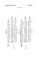
- FIGS. 9a and 9b are a block diagram of one preferred embodiment of a decoding system in accordance with the principles of the subject invention.
- FIG. 10 is a more detailed block diagram of a portion of the decoding system for FIG. 90;
- FIGS. 11 and 12 are block diagrams of inphase and quadrature multiplier units respectively, which may be utilized in the decoder system of FIGS. 90 and 9b;
- FIG. 13 is a block diagram of a control network which may be utilized in the decoder system of FIGS. 9a and 9b;
- FIGS. 14, 15, 16 and 17 are block diagrams of switching circuits adaptable for incorporation into the decoder system of FIGS. 9a and 9b;
- FIG. 18 is a block diagram of an output signal gating circuit adapted for use in conjunction with the decoding system of FIGS. 9a and 9b;
- FIG. 19 is a graph of one amplitude weighting function suitable for explaining the features of the decoding units of FIGS. 9a and 9b related to reducing the spectral sidelobes" of the decoded signal.
- FIG. 1 shows in greatly simplified terms one such application wherein the terrain 20 includes closely spaced reflector elements a, b and 0 within the pattern 22 of an antenna 24. If it is assumed that the transmitted energy pulse is as shown by a waveform 26 in FIG. 2, waveforms 28a, 28b and 28c of FIG. 2 show the return signal from the reflectors of FIG. 1 designated by the same letter; and waveform 28 the composite received video signal. Dashed line 30 depicts the shape of signal 28 after processing by a receiver of limited bandwidth, and as may be seen from envelope 30 the range of the individual reflectors could not be determined simply from the amplitude of the composite signal 28.
- the transmitted pulse 26 were first phase encoded with a suitable code, range resolution may be greatly enhanced and by way of example the transmitted pulse 26 is shown at an expanded time scale in FIG. 3 as encoded by a Frank code having four phase states and 16 encoded elements.
- the Frank code is well known in the art and will be discussed in greater detail hereinafter.
- the phase encoded on each of the elements within pulse 26 is indicated in the FIG. 3 and may be determined from the matrix of Table I as read from left to right progressing from the top to the bottom row.
- the relative phase of the transmitted energy contained within pulse 26 may be represented by vector 32 of length A referenced to an XY coordinate system.
- the coordinate system (X,Y) is assumed to rotate at an angular frequency f,,, equal to the fundamental frequency of the transmitted pulse.
- a phase advance of X degrees may be mechanized by phase delay of 21r-X degrees.
- a phase rotation equal to but opposite to the phase encoded during transmission is impressed on the received signal (multiplication by the complex conjugate of the encoded value). If the received signal 28 were applied to a shift register such that all the signal elements of the signal reflected from one of the reflectors, such as the reflector b for example, were contained within the shift register then the range interval corresponding to the area containing the reflector b could be examined by providing the appropriate decoding phase shift.
- This decoding process may be visualized by referring to FIG. 5a, 5b and 50 wherein each of the returned signals 28a, 28b and 28c respectively are decoded as though they were separately processed. If it is assumed that the signals are processed in a linear manner prior to the decoding step an analysis of each signal separately and a combination of results thereof is indicative of the results of the simultaneous processing of the signals (Superposition Theorem). It is assumed that the signal elements of the received signal 28 are shifted into 16 stage registers 34a, 34b and 340 so that the signal elements associated with each reflector are stored within the correspondingly labeled register.
- the received signal components are illustrated as being separately processed in registers 34, multiplication units 38 and summers 42 bearing postscripts corresponding to the component signal from the reflector designated by the same letter it being understood that in actuality one unit simultaneously processes the composite signal 28.
- the signal elements S through S associated with reflector b are shown in FIG. 5b as being stored in the register 34b.
- the relative phase of each received signal elements is indicated by vector arrows such as arrow 36b.
- a phase rotation equal in magnitude but opposite in direction to that impressed upon the transmitted signal is required.
- This phase rotation may be produced in a complex multiplication unit 38b which produces the phase shift indicated therein which is opposite to the phase shift impressed on transmitted signal 26.
- Complex multiplication units will be described in detail subsequently during the explanation of the decoder unit of FIG. 9.
- the output of the multiplication unit 38b (phase indicated by arrows such as 4017) is applied to a complex summation unit 42b and the sum produced by this unit is indicated at the output thereof as a vector with an amplitude 16 times that of:each element of the signal 28b and at a relative phase angle of zero (165).
- each element of the same stage (rank) of shift register 34 receives the same phase rotation in the multiplier unit 38.
- the signals associated with reflectors a and c are at a different relative position in the registers and are decorrelated whereas the signals from the reflectors b are centered in the register and are correlated.
- the code elements in the register 34c are each shifted one position to the left of the elements of the register 34b.
- the reflected energy from the range interval being correlated (reflector b) is enhanced and the energy value from the adjacent uncorrelated range intervals (b and c) are substantially attenuated.
- One of the more important characteristics of a decoding system for utilization in pulse compression applications is the ratio of the signal value originating from reflectors within a particular range interval being examined to the energy received from contiguous range intervals. It is noted that some of the energy in the decoded output signal for a particular range interval not only originates within adjacent range intervals but also some of the energy is received from other range intervals within the equivalent range of the transmitted pulse.
- sidelobe energy is the sum of the energy present in the output signal for a particular range interval which originated from reflectors located in other range intervals. It may be shown that significant sidelobe energy is produced by signals from the extreme positions of the transmitted pulse equivalent range zone.
- the subject invention is adaptable to providing amplitude weighting" during the decoding processing to reduce the effect of reflecting sources at the ends of the effective pulse length range interval.
- the selection of the type of code for pulse compression applications involves such considerations as maximizing range resolution (a large signal to sidelobe ratio) while at the same time keeping mechanization costs within reasonable limits.
- the method and mechanization in accordance with the subject invention makes it possible to accurately, reliably and economically decode and amplitude weight received reflected signals encoded with a polyphase code having equal subsequence lengths (the number of signal elements comprising each sequence are the same) and having a constant phase slope throughout each subsequence.
- One such code type which may be readily encoded onto the transmitted signal and which has been demonstrated to provide adequate range resolution comprises N signal elements with N discrete phase states equally dividing 360.
- W exp (j 21r/N) and the element in the kth row and the pth column is designated W.
- the notation W represents s which is equal to the cos (21r/N)kp +j sin (21r/N)kp and as will become apparent during the subsequent explanation of the mechanization of the subject invention multiplication by the last mentioned term is the same as a vector phase rotation of (21r/N)kp degrees.
- a phase shift of 45 may be mechanized by a multiplication by the complex quantity (1 j)/ V2.
- the decoding sequence for the code matrix may be obtained by reading the top row first and then the bottom row up to the top row with each row being read from left to right.
- the decoder unit in accordance with the subject invention will be illustrated in respect to the relatively simple Frank" code of length 16 of Table I.
- the basic phase shift is 21r/ m radians which is equal to 90 and corresponds to complex multiplication by the operatorj ⁇ f T.
- the Frank" code for example of N 16 is given in the form of complex numbers in Table IV and the corresponding decoding or phase correlation function is given in Table V.
- K and K are the values of the beginning and end points of the segment respectively.
- the net correlation function is the term by term product of the amplitude weighting and phase correlation functions of Tables V and VI respectively, and is listed in Table VII for the Frank" code of N I6.
- Nth output signal from the decoder system of the subject invention may be defined by the equation:
- Equation (2) may be mechanized as discussed hereinafter relative to FIGS. and 9b and the digital mechanization which is the subject of this invention results in a substantial reduction in the number of arithmetic operations necessary to amplitude weight and phase decode sequences of groups of N phase encoded signals.
- the mechanization in accordance with the subject invention requires a shift register having only N 1 output terminals as contrasted with a requirement for N output terminals in some prior art decoding systems.
- the number of required output leads is a significant factor in determining the size and economy of circuit devices and hence a design which significantly reduces the number of output taps possesses an economic advantage due to this feature alone.
- each group of received signal elements corresponds to only one range interval and for a typical such application of for example 2 range intervals, the reduction in arithmetic operations results in significant processing savings (equipment or processor time).
- a radar system suitable for transmitting a suitable polyphase encoded signal and for receiving and processing the reflected return video signal groups in accordance with the invention will first be described.
- a master oscillator 50 provides a high frequency signal at a frequency f to a synchronization (sync) generator 52.
- Generator 52 which may comprise conventional differentiation and pulse shaping networks, provides a series of sync pulses (waveform 54 of FIG. 8) to a pulse counter 56.
- Counter 56 is coupled to a logic network 58 on composite lead 60.
- Network 58 includes suitable conventional logic circuits for providing enable signals to selected output leads during preselected counts of the counter 56.
- the counter 56 After the counter 56 reaches its maximum count, for example 2048, it automatically resets to zero.
- Network 58 senses the zero count and applies an enable signal (1 level) to the J terminal of a control flip-flop 62.
- the Q output terminal of flip-flop 62 is coupled to a driver or power amplifier device 64.
- the device 64 may be any type of gated RF amplifier-assembly and may include a transistor amplifier or traveling wave tube (TWT). Device 64 is mechanized such that it is enabled (provides an RF output: pulse) during the time period that the flip-flop 62 is in the set state.
- TWT traveling wave tube
- Logic circuit 58 provides a 1 level signal to the K terminal of the flip-flop 62 when the counter 56 reaches the count of 15. Hence, after 16 counts, the Q output terminal of the flip-flop 62 switches to the zero level and the driver 64 is disabled (no output signal is generated).
- the input signal to the driver unit 64 is applied from the frequency multiplication unit 66 which unit steps up the frequency applied thereto from the master oscillator 50 (by the generation of harmonic frequencies in a nonlinear device and filtering, for example).
- a gated output signal at frequency f, (waveform 72 of FIG. 8) is applied to a phase shift network 70 on a lead 68 during the time period that flipflop 62 is set, i.e., for the first 16 synchronization time periods out of every 2,048 sync periods, for example.
- the phase shift network 70 is controlled in response to the logic network 58 to encode the RF pulses 72 in accordance with the polyphase code specified in Table I.
- Logic network 58 may comprise conventional gate circuits for sensing each count from through and for enabling the proper combination of phase shifter on each count.
- the required phase shifts may be mechanized with only two phase shift units 76 and 78. These units could comprise RF waveguide sections with diodes or varactors coupled thereacross so that the specified phase shift is added when an enabling signal is applied to the respective units.
- the unit 76 will provide a 90 phase shift when enabled and a 0 phase shift when disabled.
- the required phase shifts are obtained by the proper combination of only two phase shift units and the 270 phase shift may be obtained by enabling both of the units 76 and 78.
- phase modulated output signal from the phase shift unit 70 is amplified in final RF amplifier stage 80, which may include a cross field amplifier (CPA) or TWT, for example, to the final power level and is then coupled through duplexer unit 82 to transmission and reception antenna 20.
- final RF amplifier stage 80 which may include a cross field amplifier (CPA) or TWT, for example, to the final power level and is then coupled through duplexer unit 82 to transmission and reception antenna 20.
- the RF energy received from reflectors within the antenna pattern 22 is applied from antenna through duplexer 82 to a mixer 84.
- the RF reference signal to the mixer 84 is applied thereto from a stable local oscillator 86, and the mixer translates the received RF energy to the intermediate (IF) frequency band.
- the output signal from the mixer 84 is applied to and amplified by IF amplifier 88.
- the output signal from amplifier 88 is phase detected against an intermediate frequency signal from reference oscillator 90 in a phase detector 92. If the received input signal from the phase detector 92 is represented by a vector of length A with a phase B relative to the phase of the signal applied from oscillator 90 (arbitrarily established phase standard), then the output of detector 92 may be represented by the quantity A cos B which is sometimes hereinafter designated l for inphase received video.
- the signal from IF amplifier 88 is applied to a quadrature phase detector 94.
- the reference signal from oscillator 90 after being phase shifted 90 by phase shifter 96, isapplied as the reference signal to the phase detector 94.
- the output signal of detector 94 is translated 90 degrees from that of detector 92 and may be represented by the quantity A sin B which quantity is sometimes hereinafter designated Q for received quadrature video.
- the length of the range zone to be examined by the processing sections of the receiver For example, the height of the antenna, the antenna pattern and look-down angle control which range zones are illuminated by the transmitted energy.
- the interpulse period T (see FIG. 8) is subdivided into 2,048 range intervals and that the range zone to be examined by the processing portion of the system is the center 512 range intervals of each transmission period.
- a minimum/maximum range gate (waveform 99 of FIG. 8) which is at the 1 level between the minimum and maximum ranges of interest, is generated by a flipflop 98 (FIG. 6) in response to enabling signals applied from logic network 58. For example, if the J terminal of flip-flop 98 is enabled when counter 56 reaches a count of 768 and the K terminal enabled at the count of 1,280 then 512 range resolution cells would be included 7 within the range zone of interest.
- analog to digital converter units 100 and 102 Upon the application of sync pulses during the minimum/maximum range gate period (sampling periods), analog to digital converter units 100 and 102 sample the inphase and quadrature video signals respectively applied thereto from detectors 92 an 94. Units 100 and 102 convert video signals to digital words of the desired precision, e.g., each word could comprise eight bits including sign bit.
- the minimum/maximum range gate signal is combined with the sync pulses (waveform 54) in an AND gate 104 (FIG. 6) and the output signal of this gate (sampling pulses) is applied to converters 100 and 102 for synchronization thereof.
- the digital words representative of the digital value of the inphase and quadrature signals are applied from the converter units on composite leads 105 and 106 respectively to buffer storage units 108 and 110.
- the inphase and quadrature binary words are shifted out of the bufier units 108 and 110 to decoder unit 112 on composite leads 114 and 116 respectively in response to shift signals applied to the buffer storage units from the decoder unit.
- buffer storage units allow the decoding unit 112 to operate at a reduced processing rate.
- these buffers may be eliminated and the decoding unit operated at the sampling rate.
- data is stored in the buffer storage units under the control of the sampling pulses from AND gate 104 during the minimum/maximum range gate periods and retrieval of data is controlled by the decoder 112 during the interpulse period exclusive of the minimum/maximum range period.
- FIGS. 90 and 91 One preferred embodiment of the decoding unit 112 which exhibits the aforementioned advantages of increased accuracy and a reduction in the heretofore required number of arithmetic operations is shown in FIGS. 90 and 91). These two last mentioned figures together illustrate one preferred embodiment of the decoding unit and will sometimes hereinafter be generally referred to as FIG. 9. As there shown, the unit and each quadrature word respectively.
- Fixed value (multiplier values stored in unit) complex multipliers 208 and 210 are associated with stages designated 16 and 12 respectively of shift register 200.
- the output signal of multiplier 208 is applied in parallel to a W switch 212, a Z switch 214, an A accumulator". 216 and to a. B accumulator" 217.
- the output signal of multiplier 210 is coupled in parallel to Y switch 218,- W
- the organization and mechanization of the subsections 202 through 205 inclusively are quite similar and hence corresponding elements of the sections 203, 204 and 205 are given the same reference numeral as the corresponding element in section 202, followed by letter a, b or c respectively.
- the W switch in section 202 is designated 212 while the corresponding switch in section 203 is designated 212a; in section 204 it is designated 2l2b; and in section 205 the corresponding W switch is designated 212c.
- the output signal from A channel accumulator 216 is applied to a second input terminal of W switch 212 and the output from this switch is coupled in parallel to an A channel storage register 220 and to a sub-accumulation output X switch 222.
- the output signal from B channel accumulator 217 is applied on a lead 236 to Z switch 214 and the output from switch 214 is coupled in parallel to a 8 channel storage register 221 and to a second input terminal of the sub-accumulation output X switch 222 on a lead 201.
- the output signal from X switch 222 is applied on a lead 224 to a final summer 226.
- the output signal from A storage register 220 is applied through a fixed value multiplier 228 to a second input terminal of A accumulator 216 and one of the output terminals of Y switch 218 is applied to a subtrahend input terminal of A accumulator 216 on lead 203.
- the output signal of B register 221 is applied through a multiplier 229 to one input terminal of B accumulator 217 and a second output terminal of Y switch 218 is coupled to a subtraction input terminal of B accumulation unit 217.
- Multiplication units 230, 232 and 234 are coupled to the stages 8, 4, and 0 respectively of shift register 200. Subsections 203, 204 and 205 are coupled between multiplier pairs 210, 230; 230, 232; and 323, 234
- the output sub-accumulation signal from section 203 is coupled from X switch 222a on composite lead 224a to one of the input terminals of final summer 226.
- the subaccumulation' signal (the output signal) from section 204 is applied from X switch 222b toanother one of the input terminals of summer 226 on a lead 2241:; and the sub-accumulation output signal from X switch 224a is applied on a lead 224C to a fourth input terminal of final summer 226.
- the output signal from summer 226 is applied on a lead 236 to an output gating circuit 271 (1 1G518) and from there to a utilization device such as a display unit or computer unit (not shown).
- FIG. 10 A register 220, multiplier 228, A accumulator 216, and the switching units and input signals as sociated therewith are shown in greater detail in FIG. 10.
- the W switch 212 is shown in FIG. 10 as comprising two sections, an inphase section and quadrature section, with the inphase component of the signal from accumulator 216 applied on a'composite lead 219i and the quadrature portion of this signal applied on a composite lead 219G.
- the coupling of the output signal from the multiplier 208 is shown with an inphase component applied on lead 2091 to the inphase section of the W switch 212 and the:quadrature component of the output signal from the multiplier 208 applied on a lead 2090 to the quadrature section of the W switch 212.
- the W switch 212 will be explained in greater detail hereinafter relative to FIG. 14 but for the discussion relative to FIG. 10 it may be assumed that the leads (one for each bit of the inphase and quadrature word) from either multiplier 208 or accumulator 216 are selectively switched through the unit 212 in response to a control signal (not shown in FIGS. 9 and 10) applied thereto.
- the inphase and the quadrature components of a selected one of the digital words to X switch 222 are coupled to inphase and quadrature input terminals respectively of the summer 226.
- the inphase and quadrature output signals of the W switch 212 are applied to the inphase and quadrature sections respectively of the A register 220 for storage. During the next processing cycle these last mentioned signals are applied through multiplier 228 to the input terminals of inphase and quadrature sections of the A accumulator 216.
- the inphase and quadrature signals are essentially processed in parallel and the leads coupling said signals between units are given the same numerical designation as the corresponding composite leads shown in FIG. 9 except that the inphase and quadrature channels are identified by the letters I and Q respectively.
- all leads shown in FIGS. 9 and 10 are of course composite leads and all of the terminals are composite terminals for parallel processing the plurality of bits associated with each of the inphase and quadrature signals.
- a clock generator unit generates timing pulses such that data from the required number of range intervals, for example, 512 range intervals per interpulse period are processed during each processing interval (PI, see
- waveform 133 of FIG. 8 The pulses from clock generator 130 are combined in AND gate 135 with the 6 output pulses of flip-flop 98 (FIG. 6) to provide gated clock pulses c to all units of FIGS. 9 and 10.
- the leads for applying clock pulses are not shown in FIGS. 9 and 10 nor are the control lead for the W, X, Y and Z switches.
- the mechanization for controlling the switches is disclosed hereinafter and shown in FIGS. 14, 15, 16 and 17.
- the processing time interval is the complement of the storage period defined by the minimum/maximum range gate (waveform 99).
- the gated clock pulses from AND gate 135 are also applied to buffer units 108 and 110 (FIG. 7) to initiate the shifting of the digital words from these units to the inphase and quadrature channels of shift register 200.
- the operation of the complex multiplier units shown in the mechanization of FIG. 9 may be explained by first recalling that the product of two complex numbers, for example, complex numbers S j S and 142! j 14201 1441 1421 1440 1420 j( H4Q 142! S S where S and S are the inphase and quadrature component terms of a first complex number S and S are the inphase and quadrature terms of a second complex number; and (S S S S S and (S S S S are the inphase and quadrature terms respectively of the complex product of these two complex numbers.
- the inphase and quadrature sections of the multiplier units shown in FIG. 9 may be mechanized to form these product term components as indicated by sections 1401 and 1400 of FIGS. 11 and 12 respectively.
- multiplier units 146 and 148 which may be conventional digital multipliers, form the terms S S and S S respectively and the latter term is subtracted from the former term in a subtraction unit 150 to form the inphase term of the complex product.
- multiplier units 152 and 154 form the terms S S and S S respectively and these terms are combined in adder 156 to form the quadrature term of the complex product. 7
- Network 242 includes switchable conventional logic circuits for providing switch control signals S S 8,, 8,; S,,, S, and S, and S, for controlling switches W, X, Y and Z respectively according to a selected count pattern.
- the count pattern logic which is repetitive every 2N processor clock pulses, will be explained hereinafter relative to the feature of the subject invention for reducing error build-up.
- Counter 240 may be any suitable conventional counter of the type wherein after it reaches its maximum count (2N in the illustrated embodiment) it resets to zero.
- Logic network 242 may include separate flip-flop circuits (not shown, but referred to hereinafter as W, X, Y and Z) associated with correspondingly labeled pairs of control signals and which are set and reset on selected counts of the counter 240.
- each stage (for switching one data bit) of W switch 212 may be mechanized as shown in FIG. 14.
- one of the data bits from multiplier 208 applied to the W switch on the composite lead 209 is combined in AND gate 246 with the signal S from logic network 242.
- the leads shown in FIGS. 14, 15, 16 and 17 and designated by reference numerals corresponding to the composite leads of FIG. 9 are but one lead associated with one bit of the digital word applied on the corresponding composite lead.
- the corresponding data bit from the output of A accumulator 216 is combined with the 8,, output signal of network 242 in an AND gate 244.
- the output signals from the AND gate 244 and 246 are combined in an OR gate 248 and the output signal from this OR gate is applied in parallel to A register 220 and X switch 222.
- the mechanization and control of the other W switches shown in FIGS. and 9b are identical to that just described relative to FIG. 14.
- the Y switch 218 of subsection 2G2 applies the output signal from multiplier 210 to the subtrahend input terminal of either A accumulator 216 or B accumulator 217. As shown in FIG. 16 the Y switch 218 may be mechanized (the mechanization for one bit shown) by applying the output signal from the multiplier 210 to an input terminal of each of two AND gates 250 and 252.
- the S, output terminal of logic network 242 is coupled to the other input terminal of AND gate 250 and the s, output of network 242 is applied to the second input terminal of AND gate 252.
- the output signal of AND gate 250 is applied on a lead 203 to the A accumulator 216 and the output signal of the AND gate 252 is applied on a lead 233 to B accumulator 217
- the mechanization of one stage (the mechanization for one bit) of a Z switch such as switch 214 is shown in FIG. 17.
- input signals applied on a pair of input leads 235 and 236 to AND gate 254 and 256 respectively are selectively coupled by means of an OR gate 258 to an output lead 215.
- the gates 254 and 256 are controlled by S, and S signals applied from logic network 242.
- FIG. 15 shows a mechanization of one stage an X switch such as switch 222 utilized in the mechanization of subsection 202, for applying the output signals from the W or from the Z switch to the final summer 226.
- input signals applied on leads 213 and 215 to AND gates 260 and 262 respectively are controlled in response to the S and S, signals from network 242 and one of said signals is coupled through the OR gate 263 to the final summer on a lead 224.
- N processing cycles are required to produce an output signal representative of the amplitude weighted decoded value of the first encoded signal group.
- the output signal from the summer 226 is applied to the gate circuit 260 shown in FIG. 18 and this circuit is controlled so that the output signal therefrom is not gated toa utilization device (not shown) until after the first encoded signal group has been decoded.
- This feature is mechanized by controlling gate 260 with the control signal (waveform wave 181 of FIG. 8) applied from the Q output terminal of a flip-flop 268.
- Flip-flop 268 is set at a preselected count, for example, at the count of 16 (N gated clock pulses) after the reset pulse.
- Logic circuit 270 senses when the last mentioned count has been reached in counter 272 at which time a set signal is ap-
Landscapes
- Engineering & Computer Science (AREA)
- Radar, Positioning & Navigation (AREA)
- Remote Sensing (AREA)
- Computer Networks & Wireless Communication (AREA)
- Signal Processing (AREA)
- Physics & Mathematics (AREA)
- General Physics & Mathematics (AREA)
- Radar Systems Or Details Thereof (AREA)
Applications Claiming Priority (4)
| Application Number | Priority Date | Filing Date | Title |
|---|---|---|---|
| US7347070A | 1970-09-18 | 1970-09-18 | |
| GB1299173A GB1370873A (en) | 1970-09-18 | 1973-03-19 | Polyphase encoding-decoding system |
| DE19732315346 DE2315346B2 (de) | 1973-03-28 | Vorrichtung zur Korrelations-Decodierung unter Einbeziehung von Amplitudengewichtung phasenmodulierter Signale | |
| FR7311646A FR2223905B1 (OSRAM) | 1970-09-18 | 1973-03-30 |
Publications (1)
| Publication Number | Publication Date |
|---|---|
| US3731311A true US3731311A (en) | 1973-05-01 |
Family
ID=27431661
Family Applications (1)
| Application Number | Title | Priority Date | Filing Date |
|---|---|---|---|
| US00073470A Expired - Lifetime US3731311A (en) | 1970-09-18 | 1970-09-18 | Polyphase encoding-decoding system |
Country Status (3)
| Country | Link |
|---|---|
| US (1) | US3731311A (OSRAM) |
| FR (1) | FR2223905B1 (OSRAM) |
| GB (1) | GB1370873A (OSRAM) |
Cited By (23)
| Publication number | Priority date | Publication date | Assignee | Title |
|---|---|---|---|---|
| FR2240581A1 (OSRAM) * | 1973-08-10 | 1975-03-07 | Marconi Co Ltd | |
| FR2489000A1 (fr) * | 1980-08-20 | 1982-02-26 | Labo Cent Telecommunicat | Dispositif permettant de diminuer les lobes secondaires d'autocorrelation dans un radar a compression d'impulsion |
| US4353067A (en) * | 1980-08-29 | 1982-10-05 | Westinghouse Electric Corp. | Method of reducing side lobes of complementary coded pulses in a coherent pulse compression doppler radar receiving system |
| US4698827A (en) * | 1981-11-27 | 1987-10-06 | The United States Of America As Represented By The Secretary Of The Navy | Generalized polyphase code pulse compressor |
| US4734699A (en) * | 1986-04-07 | 1988-03-29 | The United States Of America As Represented By The Secretary Of The Navy | Doppler-improved polyphase pulse expander-compressor |
| US4860014A (en) * | 1987-11-25 | 1989-08-22 | The United State Of America As Represented By The Administrator Of The National Aeronautics And Space Administration | Doppler radar with multiphase modulation of transmitted and reflected signal |
| US5311193A (en) * | 1990-09-26 | 1994-05-10 | British Aerospace Public Limited Company | Digital chirp generator |
| WO1997046156A1 (en) * | 1996-06-04 | 1997-12-11 | Data Critical Corp. | Method and hand-held apparatus for demodulating and viewing frequency modulated biomedical signals |
| US6264614B1 (en) | 1999-08-31 | 2001-07-24 | Data Critical Corporation | System and method for generating and transferring medical data |
| US8301232B2 (en) | 2010-06-08 | 2012-10-30 | Alivecor, Inc. | Wireless, ultrasonic personal health monitoring system |
| US8509882B2 (en) | 2010-06-08 | 2013-08-13 | Alivecor, Inc. | Heart monitoring system usable with a smartphone or computer |
| US8700137B2 (en) | 2012-08-30 | 2014-04-15 | Alivecor, Inc. | Cardiac performance monitoring system for use with mobile communications devices |
| US9220430B2 (en) | 2013-01-07 | 2015-12-29 | Alivecor, Inc. | Methods and systems for electrode placement |
| US9247911B2 (en) | 2013-07-10 | 2016-02-02 | Alivecor, Inc. | Devices and methods for real-time denoising of electrocardiograms |
| US9254092B2 (en) | 2013-03-15 | 2016-02-09 | Alivecor, Inc. | Systems and methods for processing and analyzing medical data |
| US9254095B2 (en) | 2012-11-08 | 2016-02-09 | Alivecor | Electrocardiogram signal detection |
| US9351654B2 (en) | 2010-06-08 | 2016-05-31 | Alivecor, Inc. | Two electrode apparatus and methods for twelve lead ECG |
| US9420956B2 (en) | 2013-12-12 | 2016-08-23 | Alivecor, Inc. | Methods and systems for arrhythmia tracking and scoring |
| US9839363B2 (en) | 2015-05-13 | 2017-12-12 | Alivecor, Inc. | Discordance monitoring |
| US20180088212A1 (en) * | 2016-09-28 | 2018-03-29 | Robert Bosch Gmbh | Method for evaluating radar radiation, and radar apparatus |
| US10390758B2 (en) | 2016-03-24 | 2019-08-27 | Samsung Electronics Co., Ltd. | Method and apparatus for triage and subsequent escalation based on biosignals or biometrics |
| US10945706B2 (en) | 2017-05-05 | 2021-03-16 | Biim Ultrasound As | Hand held ultrasound probe |
| CN113542927A (zh) * | 2021-07-14 | 2021-10-22 | 国网江苏省电力有限公司营销服务中心 | 一种基于线性反馈移位的远传表计唤醒方法及装置 |
Families Citing this family (1)
| Publication number | Priority date | Publication date | Assignee | Title |
|---|---|---|---|---|
| US5115247A (en) * | 1988-02-16 | 1992-05-19 | Honeywell Inc. | Frequency modulated, phase coded radar |
Citations (1)
| Publication number | Priority date | Publication date | Assignee | Title |
|---|---|---|---|---|
| US3096482A (en) * | 1957-04-11 | 1963-07-02 | Sperry Rand Corp | Phase coded signal receiver |
-
1970
- 1970-09-18 US US00073470A patent/US3731311A/en not_active Expired - Lifetime
-
1973
- 1973-03-19 GB GB1299173A patent/GB1370873A/en not_active Expired
- 1973-03-30 FR FR7311646A patent/FR2223905B1/fr not_active Expired
Patent Citations (1)
| Publication number | Priority date | Publication date | Assignee | Title |
|---|---|---|---|---|
| US3096482A (en) * | 1957-04-11 | 1963-07-02 | Sperry Rand Corp | Phase coded signal receiver |
Non-Patent Citations (1)
| Title |
|---|
| Lurin, Ely S., Proceedings of the IEEE, Correspondence, Digital Pulse Compression Using Polyphase Code, Sept. 1963, pp. 1262 1263 * |
Cited By (39)
| Publication number | Priority date | Publication date | Assignee | Title |
|---|---|---|---|---|
| FR2240581A1 (OSRAM) * | 1973-08-10 | 1975-03-07 | Marconi Co Ltd | |
| US3945010A (en) * | 1973-08-10 | 1976-03-16 | The Marconi Company Limited | Pulse compression radar |
| FR2489000A1 (fr) * | 1980-08-20 | 1982-02-26 | Labo Cent Telecommunicat | Dispositif permettant de diminuer les lobes secondaires d'autocorrelation dans un radar a compression d'impulsion |
| US4353067A (en) * | 1980-08-29 | 1982-10-05 | Westinghouse Electric Corp. | Method of reducing side lobes of complementary coded pulses in a coherent pulse compression doppler radar receiving system |
| US4698827A (en) * | 1981-11-27 | 1987-10-06 | The United States Of America As Represented By The Secretary Of The Navy | Generalized polyphase code pulse compressor |
| US4734699A (en) * | 1986-04-07 | 1988-03-29 | The United States Of America As Represented By The Secretary Of The Navy | Doppler-improved polyphase pulse expander-compressor |
| US4860014A (en) * | 1987-11-25 | 1989-08-22 | The United State Of America As Represented By The Administrator Of The National Aeronautics And Space Administration | Doppler radar with multiphase modulation of transmitted and reflected signal |
| US5311193A (en) * | 1990-09-26 | 1994-05-10 | British Aerospace Public Limited Company | Digital chirp generator |
| WO1997046156A1 (en) * | 1996-06-04 | 1997-12-11 | Data Critical Corp. | Method and hand-held apparatus for demodulating and viewing frequency modulated biomedical signals |
| US5735285A (en) * | 1996-06-04 | 1998-04-07 | Data Critical Corp. | Method and hand-held apparatus for demodulating and viewing frequency modulated biomedical signals |
| US6264614B1 (en) | 1999-08-31 | 2001-07-24 | Data Critical Corporation | System and method for generating and transferring medical data |
| US6685633B2 (en) | 1999-08-31 | 2004-02-03 | Ge Medical Systems Information Technologies, Inc. | System and method for generating and transferring data |
| US9026202B2 (en) | 2010-06-08 | 2015-05-05 | Alivecor, Inc. | Cardiac performance monitoring system for use with mobile communications devices |
| US8509882B2 (en) | 2010-06-08 | 2013-08-13 | Alivecor, Inc. | Heart monitoring system usable with a smartphone or computer |
| US8301232B2 (en) | 2010-06-08 | 2012-10-30 | Alivecor, Inc. | Wireless, ultrasonic personal health monitoring system |
| US11382554B2 (en) | 2010-06-08 | 2022-07-12 | Alivecor, Inc. | Heart monitoring system usable with a smartphone or computer |
| US9649042B2 (en) | 2010-06-08 | 2017-05-16 | Alivecor, Inc. | Heart monitoring system usable with a smartphone or computer |
| US9351654B2 (en) | 2010-06-08 | 2016-05-31 | Alivecor, Inc. | Two electrode apparatus and methods for twelve lead ECG |
| US9833158B2 (en) | 2010-06-08 | 2017-12-05 | Alivecor, Inc. | Two electrode apparatus and methods for twelve lead ECG |
| US8700137B2 (en) | 2012-08-30 | 2014-04-15 | Alivecor, Inc. | Cardiac performance monitoring system for use with mobile communications devices |
| US9254095B2 (en) | 2012-11-08 | 2016-02-09 | Alivecor | Electrocardiogram signal detection |
| US10478084B2 (en) | 2012-11-08 | 2019-11-19 | Alivecor, Inc. | Electrocardiogram signal detection |
| US9220430B2 (en) | 2013-01-07 | 2015-12-29 | Alivecor, Inc. | Methods and systems for electrode placement |
| US9579062B2 (en) | 2013-01-07 | 2017-02-28 | Alivecor, Inc. | Methods and systems for electrode placement |
| US9254092B2 (en) | 2013-03-15 | 2016-02-09 | Alivecor, Inc. | Systems and methods for processing and analyzing medical data |
| US9681814B2 (en) | 2013-07-10 | 2017-06-20 | Alivecor, Inc. | Devices and methods for real-time denoising of electrocardiograms |
| US9247911B2 (en) | 2013-07-10 | 2016-02-02 | Alivecor, Inc. | Devices and methods for real-time denoising of electrocardiograms |
| US9572499B2 (en) | 2013-12-12 | 2017-02-21 | Alivecor, Inc. | Methods and systems for arrhythmia tracking and scoring |
| US10159415B2 (en) | 2013-12-12 | 2018-12-25 | Alivecor, Inc. | Methods and systems for arrhythmia tracking and scoring |
| US9420956B2 (en) | 2013-12-12 | 2016-08-23 | Alivecor, Inc. | Methods and systems for arrhythmia tracking and scoring |
| US10537250B2 (en) | 2015-05-13 | 2020-01-21 | Alivecor, Inc. | Discordance monitoring |
| US9839363B2 (en) | 2015-05-13 | 2017-12-12 | Alivecor, Inc. | Discordance monitoring |
| US10390758B2 (en) | 2016-03-24 | 2019-08-27 | Samsung Electronics Co., Ltd. | Method and apparatus for triage and subsequent escalation based on biosignals or biometrics |
| US20180088212A1 (en) * | 2016-09-28 | 2018-03-29 | Robert Bosch Gmbh | Method for evaluating radar radiation, and radar apparatus |
| US10514443B2 (en) * | 2016-09-28 | 2019-12-24 | Robert Bosch Gmbh | Method for evaluating radar radiation, and radar apparatus |
| US10945706B2 (en) | 2017-05-05 | 2021-03-16 | Biim Ultrasound As | Hand held ultrasound probe |
| US11744551B2 (en) | 2017-05-05 | 2023-09-05 | Biim Ultrasound As | Hand held ultrasound probe |
| CN113542927A (zh) * | 2021-07-14 | 2021-10-22 | 国网江苏省电力有限公司营销服务中心 | 一种基于线性反馈移位的远传表计唤醒方法及装置 |
| CN113542927B (zh) * | 2021-07-14 | 2023-09-22 | 国网江苏省电力有限公司营销服务中心 | 一种基于线性反馈移位的远传表计唤醒方法及装置 |
Also Published As
| Publication number | Publication date |
|---|---|
| FR2223905B1 (OSRAM) | 1976-11-05 |
| DE2315346C3 (OSRAM) | 1978-04-06 |
| FR2223905A1 (OSRAM) | 1974-10-25 |
| DE2315346A1 (de) | 1974-10-17 |
| GB1370873A (en) | 1974-10-16 |
Similar Documents
| Publication | Publication Date | Title |
|---|---|---|
| US3731311A (en) | Polyphase encoding-decoding system | |
| US4042925A (en) | Pseudo-random code (PRC) surveilance radar | |
| US4158888A (en) | Fast Fourier Transform processor using serial processing and decoder arithmetic and control section | |
| US4137533A (en) | Angle/vector processed, phase-accumulated single vector rotation, variable order adaptive MTI processor | |
| US4566010A (en) | Processing arrangement for pulse compression radar | |
| US4686655A (en) | Filtering system for processing signature signals | |
| US4491930A (en) | Memory system using filterable signals | |
| US3208065A (en) | Impulse correlation function generator | |
| US2991462A (en) | Phase-to-digital and digital-to-phase converters | |
| US3617900A (en) | Digital frequency detecting system | |
| US4486850A (en) | Incremental digital filter | |
| US3717756A (en) | High precision circulating digital correlator | |
| US3046545A (en) | Rapid-correlation echo-ranging system | |
| US3030614A (en) | Telemetry system | |
| US3747099A (en) | Polyphase code system | |
| US4633426A (en) | Method and apparatus for detecting a binary convoluted coded signal | |
| US4521779A (en) | Pulse compression system | |
| US4723125A (en) | Device for calculating a discrete moving window transform and application thereof to a radar system | |
| US4875050A (en) | Generalized doppler matched binary pulse compressor | |
| US4222050A (en) | Moving target indication radar | |
| US4313170A (en) | Autocorrelation side lobe reduction device for phase-coded signals | |
| US3696235A (en) | Digital filter using weighting | |
| US3441930A (en) | Doppler radars | |
| US4153899A (en) | MTI radar system and method | |
| US3984669A (en) | Fully digital spectrum analyzer using time compression and Discrete Fourier Transform techniques |