US3710133A - Synchronization of static inverters - Google Patents
Synchronization of static inverters Download PDFInfo
- Publication number
- US3710133A US3710133A US00070718A US3710133DA US3710133A US 3710133 A US3710133 A US 3710133A US 00070718 A US00070718 A US 00070718A US 3710133D A US3710133D A US 3710133DA US 3710133 A US3710133 A US 3710133A
- Authority
- US
- United States
- Prior art keywords
- static inverter
- output
- signal
- alternate power
- power source
- Prior art date
- Legal status (The legal status is an assumption and is not a legal conclusion. Google has not performed a legal analysis and makes no representation as to the accuracy of the status listed.)
- Expired - Lifetime
Links
Images

Classifications
-
- H—ELECTRICITY
- H03—ELECTRONIC CIRCUITRY
- H03L—AUTOMATIC CONTROL, STARTING, SYNCHRONISATION OR STABILISATION OF GENERATORS OF ELECTRONIC OSCILLATIONS OR PULSES
- H03L7/00—Automatic control of frequency or phase; Synchronisation
- H03L7/06—Automatic control of frequency or phase; Synchronisation using a reference signal applied to a frequency- or phase-locked loop
-
- H—ELECTRICITY
- H02—GENERATION; CONVERSION OR DISTRIBUTION OF ELECTRIC POWER
- H02J—ELECTRIC POWER NETWORKS; CIRCUIT ARRANGEMENTS OR SYSTEMS FOR SUPPLYING OR DISTRIBUTING ELECTRIC POWER; SYSTEMS FOR STORING ELECTRIC ENERGY
- H02J9/00—Circuit arrangements for emergency or stand-by power supply, e.g. for emergency lighting
- H02J9/04—Circuit arrangements for emergency or stand-by power supply, e.g. for emergency lighting in which the distribution system is disconnected from the normal source and connected to a standby source
- H02J9/06—Circuit arrangements for emergency or stand-by power supply, e.g. for emergency lighting in which the distribution system is disconnected from the normal source and connected to a standby source with automatic change-over, e.g. UPS systems
- H02J9/062—Circuit arrangements for emergency or stand-by power supply, e.g. for emergency lighting in which the distribution system is disconnected from the normal source and connected to a standby source with automatic change-over, e.g. UPS systems for AC powered loads
-
- H—ELECTRICITY
- H02—GENERATION; CONVERSION OR DISTRIBUTION OF ELECTRIC POWER
- H02M—APPARATUS FOR CONVERSION BETWEEN AC AND AC, BETWEEN AC AND DC, OR BETWEEN DC AND DC, AND FOR USE WITH MAINS OR SIMILAR POWER SUPPLY SYSTEMS; CONVERSION OF DC OR AC INPUT POWER INTO SURGE OUTPUT POWER; CONTROL OR REGULATION THEREOF
- H02M7/00—Conversion of AC power input into DC power output; Conversion of DC power input into AC power output
- H02M7/42—Conversion of DC power input into AC power output without possibility of reversal
- H02M7/44—Conversion of DC power input into AC power output without possibility of reversal by static converters
- H02M7/48—Conversion of DC power input into AC power output without possibility of reversal by static converters using discharge tubes with control electrode or semiconductor devices with control electrode
Definitions
- ABSTRACT U.s. t 4 307/66 A system for synchronizing the static inverter enables [5 th pha i g of the out ut from a static inverter in cor- [58] Field of Search ..32l/4; 307/19, 23, 29, 64, respondence to an alternate power Supp
- the 307/66 235; 318/6 synchronized system compares the static inverter output with the alternate power source in a phase detec- [56] References and tor which outputs an error correcting signal which is UNITED STATES PATENTS used to adjust the static inverter master clock.
- This invention provides a system for comparing the output of a static inverter to an alternate power source and thereby derive a correction signal which can be used to adjust the master clock of the static inverter.
- Another object of this invention is to provide a signal for adjusting the master clock ofa static inverter.
- a further object of this invention is to provide an economical system for synchronizing a static inverter with lumped constant components.
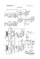
- FIG. 1 is a block diagram of a typical static inverter I used in the prior art.
- FIG. 2 is a block diagram of the preferred embodiment of the invention.
- FIG. 3 is a circuit diagram for the phase shift network and phase detector circuit of the preferred embodiment of the invention.
- FIG. 1 illustrates a block diagram of a typical static inverter used in the prior art.
- the object of a static inverter is to convert a direct current (D.C.) source into an alternating current (A.C.) source for driving equipment adapted for an A.C. source.
- a portion of the DC. source supplies the power needed to operate the static inverter while the remainder is converted into an A.C. output.
- Master clock input 2 drives flip-flop 3.
- Flip-flop 3 is connected to a square wave output inverter 4 which essentially generates half of the signal needed to obtain the desired A.C. output.
- Flip-flop 3 is also coupled to buffer flip-flop 5 which is used to drive the slave clock 6.
- Slave clock 6 drives flip-flop 7 which is coupled over to square wave output inverter 8.
- Square wave output inverter 8 essentially generates the other half of the desired A.C. output signal.
- Slave clock 6 is coupled into from variable phasing circuit 9 which provides compensation for the phase between the output of square wave output inverters 4 and 8.
- the outputs from square wave output inverters 4 and 8 are applied to reactor 10 and then to harmonic sup pressor 11 and then to filter 12.
- the output signal at terminals 13 are monitored by current limiter 14 overload voltage limiter 15, voltage limit compensator l6, and voltage limit compensator 17.
- the voltage limit compensators 16 and 17 sample the peak and valley voltage limits of the output voltage and provide information to the variable phasing circuit 9 so that the generated square waves from inverters 4 and 8 are symmetrical.
- FIG. 2 illustrates the preferred embodiment of the invention.
- the static inverter which is to be synchronized is inputted on line while the alternate or parallel power source inputs on line 101.
- Switches 20 and 21 which are mechanically coupled are closed in order to bring about the synchronization between the static inverter source in use and the alternate source to be used.
- Transformer 22 is used to step down the voltage of the static. inverter source while transformer 23 is used to step down the alternate source.
- Phase shift networks 24 and 25 are used to correct the phase relationship between the static inverter source and alternate source respectively so as to make the two inputs compatible with phase detector 26.
- Phase detector 26 and amplifier 27 receive direct current (D.C.) from power supplies 28 and 29 respectively. Power supplies 28 and 29 receive their inputs from the alternate power source.
- D.C. direct current
- phase detector 26 The inputs from phase shift networks 24 and 25 are compared in phase detector 26.
- the output from phase detector 26 is a signal which is proportional to the phase difference between the two inputs.
- This output signal is applied amplifier 27 where it is amplified and then outputs to a voltage tunable master clock 30.
- Master clock is used to supply a master clock 30 input to a static inverter such as the type illustrated in FIG. 1.
- the output from master clock 30 can be used for a three phase static inverter.
- the output from master clock 30 which is applied to flip-flop 3 of the static inverter shown in FIG. 1, changes the frequency of the outputs of inverters 4 and 8, which, in turn, produces a change in frequency at transformer 22.
- the sense of this change in frequency at transformer 22, is such as to minimize the amplitude of the output of phase-difference detector 26. Hence, the frequencies between the static inverter and the alternate power source will become synchronized.
- FIG. 3 is a circuit diagram for phase shift networks 24 and 25 and phase detector 26.
- Phase shift networks 24 and 25 areessentially similar.
- Resistors 40, 41, 42 and 43 which are across the output of transformer 23 form a voltage divider network.
- resistors 46, 47, 48 and 49 form a voltage divider for the output through transformer 22.
- Resistors 41, 42, 47 and 48 are adjustable in order to balance the outputs from transformers 23 and 22.
- phase shift 1 capacitor 51 form the phase shift control for phase shift network 24.
- the output from phase shift network 25 is coupled through resistor 52 to operational amplifier 57.
- phase shift network 24 is coupled to operational amplifier 58.
- operational amplifier 57 applies switching pulses to the base of a transistor 61 while operational amplifier 58 acts as a differential amplifier receiving input signals from both the static inverter source and the alternate power source.
- Resistor 52 and capacitor 54 produce a phase lag of 90 with respect to the input signal from the alternate power source.
- Resistors 55 and 67 are used to increase the input impedance to operational amplifier 58.
- the feedback resistor 68 with resistor 67 determines the gain of operational amplifier 58.
- Resistor 56 provides a bias and resistors 59 and 60 are balance adjustments to set operational amplifiers 57 and 58 for a zero output.
- the supply voltages V and V come from power supply 28.
- Diode 62 is used to block positive going output from operational amplifier 57 to protect transistor 61 from excessive reverse voltages.
- Resistor 63 is the load resistor for transistor 61.
- the network consisting of resistor 64 and capacitors 65 and 66 form an integrator.
- the output voltage is the integral of the voltage present at the output of operational amplifier 58 during the period of each cycle that transistor 61 is switched on. The output voltage will zero, i.e., being phase of the phase of the swing around a positive voltage, the output voltage being greater when the phase of the static inverter source lags the phase of the alternate power source and being less if the static inverter source leads.
- the output is applied to amplifier 27. Becauseof a translation in voltage between power supplies 28 and 29, the output of amplifier 27 swings plus and minus around zero of the control voltage for master clock 30.
- Amplifier 27 is of a conventional design is operative to amplify and match the output impedance of phase detector 26 to the input impedance master clock 30.
- Master clock 30 is a conventional voltage tunable oscillator whose output frequency is a function of its D.C. input voltage.
- An apparatus for synchronizing the output frequency of a static inverter with the output frequency of an alternate power source comprising phase detector means for deriving a correction voltage corresponding to the phase difference between said static inverter output and said alternate power source signal output, means for coupling a signal from said static inverter output and a signal from said alternate power source output to said phase detector means, means for sampling said correction voltage to produce a correction voltage signal, means for coupling said integrated sample correction voltage to a voltage tunable master clock and means for coupling said voltage tunable master clock to said static inverter for controlling the output frequency of said static inverter.
- An apparatus as claimed in claim 1 including means for coupling a signal from said static inverter and a signal from said alternate power comprising first and second phase shift networks for said static inverter and said alternate power source signals respectively.
- An apparatus as claimed in claim 2 wherein the means for coupling a signal from said static inverter and a signal from said alternate power source comprises first and second transformers.
- phase detector means comprises first and second operational amplifiers.
- phase detector means comprises first and second operational amplifiers.
- An apparatus as claimed in claim 7 wherein the means for integrating said sample correction voltage comprises a resistor and a capacitor.
Landscapes
- Engineering & Computer Science (AREA)
- Power Engineering (AREA)
- Business, Economics & Management (AREA)
- Emergency Management (AREA)
- Inverter Devices (AREA)
Abstract
A system for synchronizing the static inverter enables the phasing of the output from a static inverter in correspondence to an alternate power supply. The synchronized system compares the static inverter output with the alternate power source in a phase detector which outputs an error correcting signal which is used to adjust the static inverter master clock.
Description
O United States Patent 1 1111 3,710,133 Ferraro [451 Jan. 9, 1973 541 SYNCHRONIZATION 0F STATIC 3,614,461 10/1971 Speer ..307/64 INVERTERS 3,348,060 10/1967 Jamieson ..307/66 3,229,111 l/l966 Schumacher et al. .....307/66 X [75] Ralph Femm' p'scataway' 3,564,275 2/1971 Eberle ..307/29 [73] Assignee: Ward Leonard Electric Co., Inc.
Primary Examiner-William H. Beha, Jr. [221 Flled' Sept. 1970 Att0rney-Bernard Malina [21] Appl. No.: 70,718
[57] ABSTRACT U.s. t 4 307/66, A system for synchronizing the static inverter enables [5 th pha i g of the out ut from a static inverter in cor- [58] Field of Search ..32l/4; 307/19, 23, 29, 64, respondence to an alternate power Supp|y The 307/66 235; 318/6 synchronized system compares the static inverter output with the alternate power source in a phase detec- [56] References and tor which outputs an error correcting signal which is UNITED STATES PATENTS used to adjust the static inverter master clock.
- 2,594,801 4/1952 Rees ..321/l0 9 Claims, 3 Drawing Figures SYNCIIRONIZATION OF STATIC INVERTERS BACKGROUND OF THE INVENTION It is sometimes desirable to bring a static inverter into service or take one out of service either for repair or to utilize an alternate power source. In the process of introducing an alternate power source to replace the static inverter or vice versa consideration must be given to the frequencies of the two alternating currents. A difference in frequency between two power sources coupled together can result in a single signal which has the appearance of being amplitude modulated due to the power sources change phase relationship from in phase to out of phase. The presence of this modulation can seriously affect the operation of equipment such as a computer or certain types of synchronized motors. In order to eliminate the occurrence of a difference in the oscillating frequencies between the two power sources, a means of synchronization is necessary.
SUMMARY OF THE INVENTION This invention provides a system for comparing the output of a static inverter to an alternate power source and thereby derive a correction signal which can be used to adjust the master clock of the static inverter.
It is the object of the present invention to provide a system for synchronizing static inverters.
Another object of this invention is to provide a signal for adjusting the master clock ofa static inverter.
A further object of this invention is to provide an economical system for synchronizing a static inverter with lumped constant components.
Other and further objects of this invention will be obvious upon the understanding of the illustrative embodiment about to be described or will be indicated in the apended claims and various advantages not referred to herein will occur to one skilled in the art upon employment of the invention in practice.
BRIEF DESCRIPTION OF THE DRAWINGS A preferred embodiment of the invention has been chosen for purposes of illustration and description and it is shown in the accompanied drawing forming a part of the specification wherein:
FIG. 1 is a block diagram of a typical static inverter I used in the prior art.
FIG. 2 is a block diagram of the preferred embodiment of the invention.
FIG. 3 is a circuit diagram for the phase shift network and phase detector circuit of the preferred embodiment of the invention. I
FIG. 1 illustrates a block diagram of a typical static inverter used in the prior art. The object of a static inverter is to convert a direct current (D.C.) source into an alternating current (A.C.) source for driving equipment adapted for an A.C. source. A portion of the DC. source supplies the power needed to operate the static inverter while the remainder is converted into an A.C. output.
The operation of the static inverter is as follows:
The outputs from square wave output inverters 4 and 8 are applied to reactor 10 and then to harmonic sup pressor 11 and then to filter 12. The output signal at terminals 13 are monitored by current limiter 14 overload voltage limiter 15, voltage limit compensator l6, and voltage limit compensator 17. The voltage limit compensators 16 and 17 sample the peak and valley voltage limits of the output voltage and provide information to the variable phasing circuit 9 so that the generated square waves from inverters 4 and 8 are symmetrical.
FIG. 2 illustrates the preferred embodiment of the invention. The static inverter which is to be synchronized is inputted on line while the alternate or parallel power source inputs on line 101. Switches 20 and 21 which are mechanically coupled are closed in order to bring about the synchronization between the static inverter source in use and the alternate source to be used. Transformer 22 is used to step down the voltage of the static. inverter source while transformer 23 is used to step down the alternate source. Phase shift networks 24 and 25 are used to correct the phase relationship between the static inverter source and alternate source respectively so as to make the two inputs compatible with phase detector 26. Phase detector 26 and amplifier 27 receive direct current (D.C.) from power supplies 28 and 29 respectively. Power supplies 28 and 29 receive their inputs from the alternate power source.
The inputs from phase shift networks 24 and 25 are compared in phase detector 26. The output from phase detector 26 is a signal which is proportional to the phase difference between the two inputs. This output signal is applied amplifier 27 where it is amplified and then outputs to a voltage tunable master clock 30. Master clock is used to supply a master clock 30 input to a static inverter such as the type illustrated in FIG. 1. In addition, the output from master clock 30 can be used for a three phase static inverter. The output from master clock 30 which is applied to flip-flop 3 of the static inverter shown in FIG. 1, changes the frequency of the outputs of inverters 4 and 8, which, in turn, produces a change in frequency at transformer 22. The sense of this change in frequency at transformer 22, is such as to minimize the amplitude of the output of phase-difference detector 26. Hence, the frequencies between the static inverter and the alternate power source will become synchronized.
FIG. 3 is a circuit diagram for phase shift networks 24 and 25 and phase detector 26. Phase shift networks 24 and 25 areessentially similar. Resistors 40, 41, 42 and 43 which are across the output of transformer 23 form a voltage divider network. Similarly, resistors 46, 47, 48 and 49 form a voltage divider for the output through transformer 22. Resistors 41, 42, 47 and 48 are adjustable in order to balance the outputs from transformers 23 and 22.
Functionally, operational amplifier 57 applies switching pulses to the base of a transistor 61 while operational amplifier 58 acts as a differential amplifier receiving input signals from both the static inverter source and the alternate power source. Resistor 52 and capacitor 54 produce a phase lag of 90 with respect to the input signal from the alternate power source. Resistors 55 and 67 are used to increase the input impedance to operational amplifier 58. The feedback resistor 68 with resistor 67 determines the gain of operational amplifier 58. Resistor 56 provides a bias and resistors 59 and 60 are balance adjustments to set operational amplifiers 57 and 58 for a zero output. The supply voltages V and V come from power supply 28.
Diode 62 is used to block positive going output from operational amplifier 57 to protect transistor 61 from excessive reverse voltages. Resistor 63 is the load resistor for transistor 61. The network consisting of resistor 64 and capacitors 65 and 66 form an integrator. The output voltage is the integral of the voltage present at the output of operational amplifier 58 during the period of each cycle that transistor 61 is switched on. The output voltage will zero, i.e., being phase of the phase of the swing around a positive voltage, the output voltage being greater when the phase of the static inverter source lags the phase of the alternate power source and being less if the static inverter source leads. The output is applied to amplifier 27. Becauseof a translation in voltage between power supplies 28 and 29, the output of amplifier 27 swings plus and minus around zero of the control voltage for master clock 30.
As various changes may be made in the form of construction and arrangement of the parts herein without departing from the spirit and scope of the invention and without sacrificing any of its advantages it is to be understood that all matter herein is to be interpreted as illustrative and not in a limiting sense.
Having thus described my invention, 1 claim:
1. An apparatus for synchronizing the output frequency of a static inverter with the output frequency of an alternate power source comprising phase detector means for deriving a correction voltage corresponding to the phase difference between said static inverter output and said alternate power source signal output, means for coupling a signal from said static inverter output and a signal from said alternate power source output to said phase detector means, means for sampling said correction voltage to produce a correction voltage signal, means for coupling said integrated sample correction voltage to a voltage tunable master clock and means for coupling said voltage tunable master clock to said static inverter for controlling the output frequency of said static inverter.
2. An apparatus as claimed in claim 1 including means for coupling a signal from said static inverter and a signal from said alternate power comprising first and second phase shift networks for said static inverter and said alternate power source signals respectively.
3. An apparatus as claimed in claim 2 wherein the means for coupling a signal from said static inverter and a signal from said alternate power source comprises first and second transformers.
4. An apparatus as claimed in claim 1 wherein the phase detector means comprises first and second operational amplifiers.
5. An apparatus as claimed in claim 3 wherein the phase detector means comprises first and second operational amplifiers.
6. An apparatus as claimed in claim 1 wherein the means for sampling said correction voltage comprises a transistor.
7. An apparatus as claimed in claim 5 wherein the means for sampling said correction voltage comprises a transistor.
8. An apparatus as claimed in claim 1 wherein the means for integrating said sample correction voltage comprises a resistor and a capacitor.
9. An apparatus as claimed in claim 7 wherein the means for integrating said sample correction voltage comprises a resistor and a capacitor.
Claims (9)
1. An apparatus for synchronizing the output frequency of a static inverter with the output frequency of an alternate power source comprising phase detector means for deriving a correction voltage corresponding to the phase difference between said static inverter output and said alternate power source signal output, means for coupling a signal from said static inverter output and a signal from said alternate power source output to said phase detector means, means for sampling said correction voltage to produce a correction voltage signal, means for coupling said integrated sample correction voltage to a voltage tunable master clock and means for coupling said voltage tunable master clock to said static inverter for controlling the output frequency of said static inverter.
2. An apparatus as claimed in claim 1 including means for coupling a signal from said static inverter and a signal from said alternate power comprising first and second phase shift networks for said static inverter and said alternate power source signals respectively.
3. An apparatus as claimed in claim 2 wherein the means for coupling a signal from said static inverter and a signal from said alternate power source comprises first and second transformers.
4. An apparatus as claimed in claim 1 wherein the phase detector means comprises first and second operational amplifiers.
5. An apparatus as claimed in claim 3 wherein the phase detector means comprises first and second operational amplifiers.
6. An apparatus as claimed in claim 1 wherein the means for sampling said correction voltage comprises a transistor.
7. An apparatus as claimed in claim 5 wherein the means for sampling said correction voltage comprises a transistor.
8. An apparatus as claimed in claim 1 wherein the means for integrating said sample correction voltage comprises a resistor and a capacitor.
9. An apparatus as claimed in claim 7 wherein the means for integrating said sample correctioN voltage comprises a resistor and a capacitor.
Applications Claiming Priority (1)
| Application Number | Priority Date | Filing Date | Title |
|---|---|---|---|
| US7071870A | 1970-09-09 | 1970-09-09 |
Publications (1)
| Publication Number | Publication Date |
|---|---|
| US3710133A true US3710133A (en) | 1973-01-09 |
Family
ID=22096968
Family Applications (1)
| Application Number | Title | Priority Date | Filing Date |
|---|---|---|---|
| US00070718A Expired - Lifetime US3710133A (en) | 1970-09-09 | 1970-09-09 | Synchronization of static inverters |
Country Status (1)
| Country | Link |
|---|---|
| US (1) | US3710133A (en) |
Cited By (5)
| Publication number | Priority date | Publication date | Assignee | Title |
|---|---|---|---|---|
| US3909621A (en) * | 1973-04-09 | 1975-09-30 | Lepaute Cie Gle Elec Ind | Method for connecting a static inverter and a power source in parallel to supply electric energy to a load and a logic device for implementing the method |
| US4010381A (en) * | 1975-04-24 | 1977-03-01 | Bell Telephone Laboratories, Incorporated | No-break ac power supply |
| WO1987000701A1 (en) * | 1985-07-16 | 1987-01-29 | Italtel Società Italiana Telecomunicazioni S.P.A. | Synchronizing circuit for a plurality of power units |
| US4841161A (en) * | 1985-07-16 | 1989-06-20 | Italtel Societa Italiana Telecomunicazioni S.P.A | Monitoring circuit for control means and selective breakaway means in modular supply systems |
| US5237208A (en) * | 1988-10-25 | 1993-08-17 | Nishimu Electronics Industries Co., Ltd. | Apparatus for parallel operation of triport uninterruptable power source devices |
Citations (5)
| Publication number | Priority date | Publication date | Assignee | Title |
|---|---|---|---|---|
| US2594801A (en) * | 1950-02-24 | 1952-04-29 | Albert R Rees | Power supply for radio sets |
| US3229111A (en) * | 1961-10-27 | 1966-01-11 | Electro Seal Corp | A.c. power system having alternate sources of supply |
| US3348060A (en) * | 1964-01-14 | 1967-10-17 | Lorain Prod Corp | Continuously-operatingstandby powersupply and battery-charging apparatus and method |
| US3564275A (en) * | 1969-05-22 | 1971-02-16 | Cons Edison Co | Frequency-responsive control circuit |
| US3614461A (en) * | 1969-08-11 | 1971-10-19 | Gen Electric Canada | Circuit for keeping the frequency of an inverter synchronized with the frequency of another source |
-
1970
- 1970-09-09 US US00070718A patent/US3710133A/en not_active Expired - Lifetime
Patent Citations (5)
| Publication number | Priority date | Publication date | Assignee | Title |
|---|---|---|---|---|
| US2594801A (en) * | 1950-02-24 | 1952-04-29 | Albert R Rees | Power supply for radio sets |
| US3229111A (en) * | 1961-10-27 | 1966-01-11 | Electro Seal Corp | A.c. power system having alternate sources of supply |
| US3348060A (en) * | 1964-01-14 | 1967-10-17 | Lorain Prod Corp | Continuously-operatingstandby powersupply and battery-charging apparatus and method |
| US3564275A (en) * | 1969-05-22 | 1971-02-16 | Cons Edison Co | Frequency-responsive control circuit |
| US3614461A (en) * | 1969-08-11 | 1971-10-19 | Gen Electric Canada | Circuit for keeping the frequency of an inverter synchronized with the frequency of another source |
Cited By (6)
| Publication number | Priority date | Publication date | Assignee | Title |
|---|---|---|---|---|
| US3909621A (en) * | 1973-04-09 | 1975-09-30 | Lepaute Cie Gle Elec Ind | Method for connecting a static inverter and a power source in parallel to supply electric energy to a load and a logic device for implementing the method |
| US4010381A (en) * | 1975-04-24 | 1977-03-01 | Bell Telephone Laboratories, Incorporated | No-break ac power supply |
| WO1987000701A1 (en) * | 1985-07-16 | 1987-01-29 | Italtel Società Italiana Telecomunicazioni S.P.A. | Synchronizing circuit for a plurality of power units |
| US4841161A (en) * | 1985-07-16 | 1989-06-20 | Italtel Societa Italiana Telecomunicazioni S.P.A | Monitoring circuit for control means and selective breakaway means in modular supply systems |
| US4886981A (en) * | 1985-07-16 | 1989-12-12 | Italtel Societa Italiana | Synchronizing circuit for a plurality of power units |
| US5237208A (en) * | 1988-10-25 | 1993-08-17 | Nishimu Electronics Industries Co., Ltd. | Apparatus for parallel operation of triport uninterruptable power source devices |
Similar Documents
| Publication | Publication Date | Title |
|---|---|---|
| US5191519A (en) | Current sharing control in a parallel inverter system | |
| US4019124A (en) | Apparatus for compensating reactive power in a three-phase network | |
| US4730243A (en) | EMI reduction circuit | |
| US3624486A (en) | Apparatus for controlling pulse width modulation of inverter circuits | |
| WO1990007230A1 (en) | Dc content control for an inverter | |
| GB2185835A (en) | Inverter control apparatus | |
| US4646221A (en) | Control circuit for inverter | |
| US3710133A (en) | Synchronization of static inverters | |
| JPS61116973A (en) | Method of controlling power converter | |
| US2547162A (en) | Electronic inverter | |
| US2464818A (en) | Frequency control system | |
| US3821652A (en) | Square to sine converter | |
| US3857108A (en) | Frequency drift compensation for a voltage controlled oscillator | |
| GB2142484A (en) | Capacitance control for a static var generator | |
| GB1567725A (en) | Calling generators for telecommunications systems | |
| US4692686A (en) | Low-distortion line voltage regulator | |
| US3396347A (en) | Precision oscillator | |
| US2654032A (en) | Automatic frequency control system | |
| US2904685A (en) | Frequency-doubling circuit arrangement | |
| US3534284A (en) | Automatic phase-locking circuit | |
| US2839719A (en) | Voltage and waveform regulator | |
| US3922593A (en) | Circuit for producing odd frequency multiple of an input signal | |
| US3792339A (en) | Control device for an inverted converter | |
| RU2016462C1 (en) | Method of synchronization of static frequency converter and a c power supply source | |
| US4287556A (en) | Capacitive current limiting inverter |