US3705357A - Morphic exclusive-or circuits - Google Patents
Morphic exclusive-or circuits Download PDFInfo
- Publication number
- US3705357A US3705357A US127114A US3705357DA US3705357A US 3705357 A US3705357 A US 3705357A US 127114 A US127114 A US 127114A US 3705357D A US3705357D A US 3705357DA US 3705357 A US3705357 A US 3705357A
- Authority
- US
- United States
- Prior art keywords
- morphic
- circuit
- exclusive
- input
- variable
- Prior art date
- Legal status (The legal status is an assumption and is not a legal conclusion. Google has not performed a legal analysis and makes no representation as to the accuracy of the status listed.)
- Expired - Lifetime
Links
- 238000012360 testing method Methods 0.000 claims abstract description 69
- 230000006870 function Effects 0.000 description 28
- 230000015654 memory Effects 0.000 description 12
- 238000001514 detection method Methods 0.000 description 11
- 238000010586 diagram Methods 0.000 description 8
- 238000013461 design Methods 0.000 description 5
- 230000000694 effects Effects 0.000 description 3
- 238000000034 method Methods 0.000 description 3
- 230000008901 benefit Effects 0.000 description 2
- 230000008859 change Effects 0.000 description 2
- 238000012937 correction Methods 0.000 description 2
- 101100037618 Neurospora crassa (strain ATCC 24698 / 74-OR23-1A / CBS 708.71 / DSM 1257 / FGSC 987) ant-1 gene Proteins 0.000 description 1
- 240000007594 Oryza sativa Species 0.000 description 1
- 241001529934 Simian T-lymphotropic virus 3 Species 0.000 description 1
- 230000000295 complement effect Effects 0.000 description 1
- 230000008878 coupling Effects 0.000 description 1
- 238000010168 coupling process Methods 0.000 description 1
- 238000005859 coupling reaction Methods 0.000 description 1
- 230000001419 dependent effect Effects 0.000 description 1
- 238000011156 evaluation Methods 0.000 description 1
- 230000000977 initiatory effect Effects 0.000 description 1
- 238000007689 inspection Methods 0.000 description 1
- SIABDLGPVODQRN-UHFFFAOYSA-N lancin Natural products COC1CC(OC2C(C)OC(CC2OC)OC3CCC4(C)C5C(O)C(O)C6(C)C(CCC6(O)C5(O)CC=C4C3)C(C)O)OC(C)C1O SIABDLGPVODQRN-UHFFFAOYSA-N 0.000 description 1
- 230000007257 malfunction Effects 0.000 description 1
- 230000008569 process Effects 0.000 description 1
- 230000000644 propagated effect Effects 0.000 description 1
- 230000001902 propagating effect Effects 0.000 description 1
- 238000011084 recovery Methods 0.000 description 1
- 230000009467 reduction Effects 0.000 description 1
- 238000013519 translation Methods 0.000 description 1
Images

Classifications
-
- H—ELECTRICITY
- H03—ELECTRONIC CIRCUITRY
- H03K—PULSE TECHNIQUE
- H03K19/00—Logic circuits, i.e. having at least two inputs acting on one output; Inverting circuits
- H03K19/007—Fail-safe circuits
Definitions
- the present invention relates to a logic circuit for testing the condition of a set of self-testing logic variables. [2!] 127d More specifically, it relates to such a logic circuit for forming an Exclusive-Or function on such variables. [52] US. Cl. ..328/93, 307/216, 328/ 159 The circuit has particular utility in high reliability [51] Int. Cl.
- H03k 19/32 H03k 19/38 systems for checking the conditions of a plurality of [58] Field of Search ..328/93, 159; 307/216 line pairs wherein each line pair constitutes a morphic self-testing variable and 'wherein the circuit output is [56] References Cited itself a morphic self-testing function.
- Errors may occur at any given point in a computing system, such as in the logical circuitry, ranging from simple switching gates to even the internal connecting cables coupling various components of the system together wherein a poor contact can cause a hard or even intermittent failure.
- a particular area in a computer which requires considerable testing is that of the computer memory; the memory is the source of both data and instructions. Due to the complexity of most computer memories, including the various addressing circuitry components, memory decoders, drivers, sense networks, amplifiers, etc., there are many possible locations in which a failure can occur. Further, a failure in this area can result in an error which will be propagated to any and all subsequent portions of the computer where the data is used. Thus it is of great importance to insure proper memory operation on either read or write access.
- the most commonly used scheme involves the use of one or more parity bits.
- the simplest is a single parity bit scheme wherein the parity bit may be set to a one or zero depending upon the character of the data which it accompanies. In some systems, it may be desired to set all parities equal to an even number of ones. Thus, if the data contains an odd number of ones, the parity bit would be chosen to be a one so that the total number of bits in the transmitted data word would always be an even number of ones.
- the same scheme may equally well be used to always insure that the total number of ones in the transmitted data word are odd.
- a parity bit may be included with the address and also with each data word stored in the memory. Thus, parity of the address may be checked and parity of the data word may ,be checked after read out.
- cuit which may be expanded to receive any desired number of self-testing logic variable pairs of morphic variable inputs.
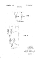
- FIG. 1 is a logical schematic diagram of a first embodiment of a two input pair morphic Exclusive-OR circuit constructed in accordance with the teachings of the present invention.
- FIG. 2 is a logical schematic diagram of a two input pair morphic Exclusive-OR circuit constructed in accordance with the principles of the present invention.
- FIG. 3 is a more detailed logical schematic diagram of the morphic Exclusive-OR block shown in FIG. 1.
- FIG. 4 illustrates a diagramatic representation of a two input pair morphic Exclusive-OR circuit (MXOR) shown in FIGS. 5 and 6.
- MXOR morphic Exclusive-OR circuit
- FIG. 5 is a logic block diagram of a three input pair morphic Exclusive-OR circuit.
- FIG. 6 is a logic block diagram of a four input pair morphic Exclusive-OR circuit.
- a morphic Exclusive-OR circuit having as inputs at least two pairs of morphic operators and having as an output a single pair of morphic operators, said circuit including means for providing a Code Space output when one and only one pair of morphic operators at the input is in Code Space and the other pair of inputs is in Error Space and providing an Error Space output when both inputs are in Code Space or Error Space.
- Code Space (CS) and Error Space (ES) may be selectively chosen from a first condition wherein a given line pair or morphic variable pair will carry a 01 or a 10 binary signal and a second condition wherein a It is a still further object to provide such a logic cir-' line pair or morphic variable pair will carry a 00 or a 1 1 binary signal, wherein if one condition represents Error Space, the other condition will represent Code Space.
- Code Space and Error Space
- CS Code Space
- Error Space are used as a convenient way to express code conditions and are not intended to be otherwise limiting. The terminology arises from the application of testing techniques discussed in the previously related two copending applications wherein a given condition on a line pair from some testing circuit indicates that everything is operating properly and the other condition implies that an Error is present, either in the circuitry or in the data being tested. It should also be noted that, in some usage and implementation, the definition of CS by 01 and I0 (and ES by 00 and 11.) will be changed to represent CS by 00 and l l (and ES by 01 and 10). The definitions above will be preserved consistently throughout this treatment.
- the present morphic Exclusive-OR circuit is quite simple in concept but is believed to be novel since no use for morphic operators as defined herein was believed to exist before the recent advent of self-testing error detection systems.
- the present morphic Exclusive-OR circuit is also self-testing in that, in the event of an internal circuit failure, a change from one code condition to the other in the output will be produced by this circuit.
- FIG. 1 there is shown the simplest version of the invention wherein the two pairs of morphic operator inputs A and B feed into the two indicated Exclusive-OR circuits and produce a single output pair.
- each of these Exclusive-OR circuits is a simple two input, single output Exclusive-OR and at first glance appears like a first level of a four input conventional Exclusive-OR tree.
- the resemblance ends as it will be noted that one of the Exclusive-ORs takes an input from the input pair A and a second input from the input pair B.
- the other Exclusive-OR does the same thing.
- the output of the circuit is a binary pair rather than a single line.
- FIG. 3 comprises a detailed logical schematic diagram of the circuit of FIG. 1 which is embodied utilizing simple AND, OR and Inverter stages. Further, a complete Truth Table and Test Detect Table III is presented showing exactly how the circuit works with various conditions of inputs and also illustrating the self-testability feature.
- FIG. 2 comprises an alternative embodiment of the two input single output morphic Exclusive-OR circuit constructed in accordance with the principles of the invention. It will be noticed that in this embodiment one circuit path comprises approximately twice as many levels of logic. This configuration of the morphic Exclusive- OR is dependent on the Algorithm required to obtain the self-testing structure. For example, for one particular Algorithm, the configuration of FIG. 1 will not necessarily give a self-testing structure in multilayer circuits but the configuration of FIG. 2 will.
- FIG. 3 comprises a detailed logical schematic diagram of the morphic Exclusive-OR circuit which is shown at a higher level of logical representation in FIG.
- FIGS. 4, 5 and 6 the functional block diagram of FIG. 4 indicated as MXOR, could be filled by either the particular circuit embodiment of FlGS. 2 or 3 as it is used in the functional context only. It applies to the way that such a morphic Exclusive-OR could be utilized in a larger configuration such as in FIGS. 5 and 6. These two FIGS. are essentially the same showing three'and four morphic variable pairs respectively and indicating the conventional way that such basic MXOR blocks would be connected to make the indicated logical test.
- the Code Space output would be produced at X for odd numbers of Code Space inputs, i.e., 1 or 3.
- This is analogous to the case of conventional Exclusive-OR circuitry used to determine parity of a set of bits. It will, of course, be appreciated that the basic 1 numn moi l.
- the embodiment of the individual Exclusive-OR circuits in FIG. 3 is the same as that in FIG. 2 as will be apparent. Again, the output of the embodiment of FIG. 3 is a line pair or morphic variable pair.
- the pair of lines may assume either of two conditions. The first is where the signal appearing on the two lines is different, i.e., 01 or 10. The second condition is that where the signal appearing on the two lines is identical, i.e., 00 or 1 1.
- the morphic Exclusive-OR circuit be essentially self-testing when located in an overall self-testing error checking system.
- the present morphic Exclusive-OR circuit is considered to be one significant member of a universal self-testing set of morphic operator blocks (the other being the morphic AND) by which it is meant that utilizing said universal set there exists an algorithm for interconnecting said blocks so as to give a self-testing implementation for any desired morphic Boolean function.
- Tables II and Ill The actual operation of the specific circuits of FIGS. 2 and 3 is set forth in Tables II and Ill respectively. These two tables are identical in form and differ only in the specified points in the circuits to which they refer. Both of these tables are what would be referred to as a combination Test Detect Table and a Truth Table. They are combined for the sake of convenience since all possible inputs are required for both portions of the table; It will be further noted that the input configurations are clearly indicated in the left-hand or Input portion of the table which, as indicated, include the two input pairs A and B, thus corresponding to the drawings. Similarly, the output pair is labeled X. Both tables are also broken into four distinct sections depending on the input code configuration.
- each table has two CS inputs to produce an ES output.
- Section two receives a CS and ES input to produce CS output.
- Section three has an ES input and a CS input and thus produces a CS output and
- section four of each table has an ES and an ES input to produce an ES output.
- the pair 01, 10 is designated as Code Space and the pair 00, l 1 is denoted as Error Space.
- Test Detect portion of Tables II and III is designed to show that the circuit is testable for stuckat failures at all of the testing points shown in the two Figures, i.e., points 1 through 14, wherein in both MXOR blocks could be cascaded into trees as shown in FIG. 6 to accomodate any number of desired morphic variable pairs on which it was desired to perform an Exclusive-OR operation.- I 7
- FIGS; 4, s and 6 completes the description of the basic concepts embodied in the present invention. It is believed that the present morphic Exclusive-OR circuit, while simple and straightforward in configuration, nevertheless performs a logic function not known in the art prior to the present application. The provision of such a basic operating block for performing Boolean logic on morphic operators is believed to have significant utility in the error detection and error correction fields.
- MXOR ,Morphic Exclusive-OR
- MMD Morphic AND
- a modified MXOR as mentioned previously, is.us ed to test two (morphic, self-testing) logic variables R and P and the (morphic, self-testing) output of the modified MXOR is referred to as Q.
- the testing circuit uses an MXOR having a morphic complement function performed on its outputs; hence, the output space definition is reversed so that the output of the testing circuithas an ES output whenever precisely one of the inputs, R and P, are in Error Space.
- This may be used to indicate either a double error detected in the output data word (the manifestation of a functional failure of the memory unit) or a failure in the circuitry producing Q (a failure in the checking circuit), including the circuitry used to produce R and P.
- a double error detected in the output data word the manifestation of a functional failure of the memory unit
- a failure in the circuitry producing Q a failure in the checking circuit
- R and P the circuitry used to produce R and P.
- the new, morphic self-testing function Z is defined by whe'reGB and are the symbols for the MXOR and morphic NOT.,Hence, Z will have an ES output anytime the inputs to the circuit producing Q are not space-wise consistent with the output state for Q. Otherwise, Z will have a CS status. While it is true that this is almost duplication, no comparator is used and the comparison is done in a self-testing fashion. Hence, a circuit failure in the circuit producing Q can be uniquely identified.
- f is multi-level in its gate structure, if it were to be implemented by ordinary logic gates. Then, if it is desired to implement this in a self'testing logic form, each input variable, a would be replaced by a variable pair, (a a However, this would not alone necessarily provide a self-testing form; in multilevel circuitry, the design of self-testing functions without the use of morphic operators is a very precarious process, usually requiring rnuch iterative design and evaluation by a circuit simulator.
- the function f(a ,a a,,,A,V,-) would become F(a, ,a ,a ,a ,a a,,,,MX- OR,MAND).
- (f f is a particular self-testing embodiment
- the embodiment (f +7 is likewise a self-testing embodiment for morphic Boolean functions.
- a morphic self-testing Exclusive-OR circuit having as inputs two morphic variable pairs and having as an output a single morphic variable pair, said circuit including means for producing a first output code condition when one and only one input morphic variable pair is in said first code condition and the other input morphic variable pair is in a second code condition and means for producing a second output code condition when both morphic variable input pairs are in said first code condition or both are in said second code condition wherein said first and second code conditions are selectively chosen from a first state wherein a given morphic variable pair comprises a 01 or a binary signal and a second state wherein a morphic variable pair comprises a 00 or a l 1 binary signal, wherein if one state represents said first code condition, the other state represents the second code condition.
- a morphic Exclusive-OR circuit as set forth in claim 2 including means for connecting the other said second Exclusive-OR circuit inputs from each of said morphic variable pairs to said second Exclusive-OR circlaim 2 including means for connecting to said second binary Exclusive-OR circuit the output of said first binary Exclusive-OR and the other input of a first of said morphic variable input pairs, and means for connecting the other input of said second morphic variable input pair directly to the output line of said morphic Exclusive-0R circuit and for connecting the single output from said second binary Exclusive-OR circuit to the other output line of said morphic Exclusive-OR circuit.
- each binary Exclusive-OR comprises two, two input AND circuits, each AND circuit having as its input the true and inverted signal appearing on the two input lines to said binary Exclusive-OR circuit and the other AND circuit having as its input the inverted and the true input signals appearing on the two input lines to said binary Exclusive-OR circuit, the outp uts of said two AND circuits being fed to a binary OR circuit, the output of said OR circuit comprising the single line output of said binary Exclusive-OR.
- a morphic Exclusive-OR system for performing a morphic Exclusive-OR function on M morphic variable input pairs, said circuit being comprised of M-l individual two input morphic Exclusive-OR blocks, said blocks being connected to said M morphic variable input pairs so that two morphic variable input pairs are 7 connected to each block and a single morphic variable cuit and means for taking the outputs from said two binary Exclusive-OR circuits to provide the output morphic variable pair for said morphic Exclusive-OR.
- each binary Exclusive-OR comprises two, two input AND circuits, each AND circuit having as its input the true and inverted signal appearing on the two input lines to said binary Exclusive-OR circuit and the other AND circuit having as its inputs the inverted and the true input signals appearing on the two input lines to said binary Exclusive-OR circuit, the outputs of said two AND circuits being fed to a binary OR circuit, the output of said OR circuit comprising the single line output of said binary Exclusive-OR.
- a morphic Exclusive-OR circuit as set forth in output pair is produced by each said block, said blocks being connected in a tree circuit configuration to produce a single morphic variable output pair from said M morphic variable input pairs and wherein each individual block comprises an individual morphic Exclusive-OR circuit including means for producing a first output code condition when one and only one input morphic variable pair is in said first code condition and the other input morphic variable pair is in a second code condition and means for producing a second output code condition when both morphic variable input pairs are in said first code condition or both are in said second code condition wherein said first and second code conditions are selectively chosen from a first state wherein a given morphic variable pair comprise a 01 or a 10 binary signal and a second state wherein a morphic variable pair comprises a 00 or a ll binary signal, wherein if one state represents said first code condition, the other state represents the second code condition.
Landscapes
- Physics & Mathematics (AREA)
- Engineering & Computer Science (AREA)
- Computer Hardware Design (AREA)
- Computing Systems (AREA)
- General Engineering & Computer Science (AREA)
- Mathematical Physics (AREA)
- Test And Diagnosis Of Digital Computers (AREA)
- Tests Of Electronic Circuits (AREA)
Applications Claiming Priority (1)
| Application Number | Priority Date | Filing Date | Title |
|---|---|---|---|
| US12711471A | 1971-03-23 | 1971-03-23 |
Publications (1)
| Publication Number | Publication Date |
|---|---|
| US3705357A true US3705357A (en) | 1972-12-05 |
Family
ID=22428378
Family Applications (1)
| Application Number | Title | Priority Date | Filing Date |
|---|---|---|---|
| US127114A Expired - Lifetime US3705357A (en) | 1971-03-23 | 1971-03-23 | Morphic exclusive-or circuits |
Country Status (3)
| Country | Link |
|---|---|
| US (1) | US3705357A (https=) |
| FR (1) | FR2131255A5 (https=) |
| GB (1) | GB1370379A (https=) |
Cited By (3)
| Publication number | Priority date | Publication date | Assignee | Title |
|---|---|---|---|---|
| US4157480A (en) * | 1976-08-03 | 1979-06-05 | National Research Development Corporation | Inverters and logic gates employing inverters |
| US5528165A (en) * | 1995-04-03 | 1996-06-18 | Sun Microsystems, Inc. | Logic signal validity verification apparatus |
| US6801585B1 (en) * | 2000-10-16 | 2004-10-05 | Rf Micro Devices, Inc. | Multi-phase mixer |
-
1971
- 1971-03-23 US US127114A patent/US3705357A/en not_active Expired - Lifetime
- 1971-11-04 FR FR7140207A patent/FR2131255A5/fr not_active Expired
- 1971-11-22 GB GB5406071A patent/GB1370379A/en not_active Expired
Cited By (3)
| Publication number | Priority date | Publication date | Assignee | Title |
|---|---|---|---|---|
| US4157480A (en) * | 1976-08-03 | 1979-06-05 | National Research Development Corporation | Inverters and logic gates employing inverters |
| US5528165A (en) * | 1995-04-03 | 1996-06-18 | Sun Microsystems, Inc. | Logic signal validity verification apparatus |
| US6801585B1 (en) * | 2000-10-16 | 2004-10-05 | Rf Micro Devices, Inc. | Multi-phase mixer |
Also Published As
| Publication number | Publication date |
|---|---|
| GB1370379A (en) | 1974-10-16 |
| FR2131255A5 (https=) | 1972-11-10 |
Similar Documents
| Publication | Publication Date | Title |
|---|---|---|
| US3755779A (en) | Error correction system for single-error correction, related-double-error correction and unrelated-double-error detection | |
| Pradhan et al. | Error-correcting codes and self-checking circuits | |
| US3585378A (en) | Error detection scheme for memories | |
| US3949208A (en) | Apparatus for detecting and correcting errors in an encoded memory word | |
| US4730320A (en) | Semiconductor memory device | |
| CA1151305A (en) | Memory write error detection circuit | |
| US4958350A (en) | Error detecting/correction code and apparatus | |
| US4388684A (en) | Apparatus for deferring error detection of multibyte parity encoded data received from a plurality of input/output data sources | |
| US3675200A (en) | System for expanded detection and correction of errors in parallel binary data produced by data tracks | |
| US4236247A (en) | Apparatus for correcting multiple errors in data words read from a memory | |
| US2973506A (en) | Magnetic translation circuits | |
| US3925647A (en) | Parity predicting and checking logic for carry look-ahead binary adder | |
| US3559167A (en) | Self-checking error checker for two-rail coded data | |
| US3602886A (en) | Self-checking error checker for parity coded data | |
| US2958072A (en) | Decoder matrix checking circuit | |
| US3825894A (en) | Self-checking parity checker for two or more independent parity coded data paths | |
| US3381270A (en) | Error detection circuits | |
| US3781796A (en) | Error detecting translator | |
| Yau et al. | Universal logic circuits and their modular realizations | |
| US3566093A (en) | Diagnostic method and implementation for data processors | |
| US3705357A (en) | Morphic exclusive-or circuits | |
| US3016517A (en) | Redundant logic circuitry | |
| US3305830A (en) | Error correcting redundant logic circuitry | |
| US3411137A (en) | Data processing equipment | |
| US3784978A (en) | Self-checking decoder |