US3576244A - Coin acceptor having resistivity and permeability detector - Google Patents
Coin acceptor having resistivity and permeability detector Download PDFInfo
- Publication number
- US3576244A US3576244A US789872A US3576244DA US3576244A US 3576244 A US3576244 A US 3576244A US 789872 A US789872 A US 789872A US 3576244D A US3576244D A US 3576244DA US 3576244 A US3576244 A US 3576244A
- Authority
- US
- United States
- Prior art keywords
- coin
- station
- coils
- channel
- enter
- Prior art date
- Legal status (The legal status is an assumption and is not a legal conclusion. Google has not performed a legal analysis and makes no representation as to the accuracy of the status listed.)
- Expired - Lifetime
Links
Images

Classifications
-
- G—PHYSICS
- G07—CHECKING-DEVICES
- G07D—HANDLING OF COINS OR VALUABLE PAPERS, e.g. TESTING, SORTING BY DENOMINATIONS, COUNTING, DISPENSING, CHANGING OR DEPOSITING
- G07D5/00—Testing specially adapted to determine the identity or genuineness of coins, e.g. for segregating coins which are unacceptable or alien to a currency
- G07D5/08—Testing the magnetic or electric properties
Definitions
- ABSTRACT A coin acceptor that detects the bulk resistivity and permeability of a coin and determines whether or not the [54] ISTIWTY AND coin is valid.
- a two-coil inductor forms one arm of a normally 9 Claims 6mm. Fi unbalanced Maxwell bridge and is disposed at a test station mg which is interposed in a channel through which the coin [52] US. Cl 194/100 passes. The two coils have series aiding magnetic fields and Cl G0 f 3/02 are disposed on opposite sides of the coin channel with the [50] Field of Search 194/6, 100, lines of force crossing the channel at generally right angles to the opposed faces of a coin under test.
- a valid coin moving through the lines of force causes the inductance to change and [56] Ree'ences C'ted effect balancing of the bridge. If this occurs throughout a FOREIGN PATENTS predetermined test period, a coin deflector below the test sta- 152,433 7/1953 Australia 194/( 100.5) i n i wi hdr wn to p rmit the coin to enter an accept path.
- the primary object of this invention to provide an improved coin acceptor of high flexibility which is capable of detecting and separating legitimate coins from counterfeit coinage without limitation as to the composition of the legitimate-coins.
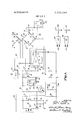
- FIG. 1 is an electrical schematic diagram of the acceptor circuitry
- FIG. 2 is a fragmentary, elevational view of a channel of the acceptor showing the test station therein;
- FIG. 3 is a verticalsectional view taken along-line 3-3 of FlG.,4"is a horizontal, sectional view taken along line 4-4 of of flat, oval-shaped coils 16-are received and'held in complemental openings in the respective plates and 12 andare disposed in direct opposition to each other as is clear in FIG. 3,
- a lead 18 is illustrated connected to the outer end of one of the coils 16, the latter comprising a single layer of turns wound one within the other and terminating at the inner end of the coil where a connection is made toalead20.
- a vertical slot 22in plate 10 is aligned with'the longitudinal axis of the oval coil 16 and is centered with'respect'thereto, there being a corresponding slot in plate 12 in alignment with slot 22.
- a light source 24 is mounted in the slot 22 and may be adjustably positioned therein depending upon the diameter of the. coin tobe tested.
- the source 24 would commonly comprise a small electrical lamp encased in a suitable housing.
- the plate 12 serves to mount a coin sensor 26 which, as will beseenhereinafter, may comprise a photo- Darlington lightdetector.
- the sensor 26 is also'movable in the slot in plate 12so that the sensor 26 maybe aligned with the source 24 as required.
- the coin vgravitates through the channel 14 it passes between the coils '16 and masks thesensor'26.
- the two coils 16 are serially connected and produce magnetic fields in series aiding relationship toeach other, as will be appreciated more fully hereinafter.
- An opening 28 in the plate 12 receives a coin deflector 30 which normally extends into the channel -14 below the teststution.ln its normal position, the deflector 30 diverts gravitating coins into a reject path 32; when the deflector 30 is withdrawn out of blocking relationship to the coins, the
- An electrical actuator in the form of an accept electromagnet 36 is mounted on plate 12 and, when energized, attracts a magneticarm 38 connected to deflector 30 that is pivotally carried by a projecting support'member 40.
- the inductor comprising the two coils 16 forms one arm of a Maxwell bridge 42 having a second, resistive arm 44, a third arm '46 containing adjustable resistors and a parallel capacitor, and a fourth arm 48 containing a pair of serially connected adjustable resistors.
- a sinusoidal oscillator stage 54 has an output connection 56 which extends to the bridge input 50 through a variable resistor 58.
- the other output connection of the oscillator stage 54 is-illustrated by the ground symbol-and hence is connected to the grounded bridge input52.
- a power lead for the stage 54 is illustrated at 60.
- the two terminals labeled +V represent connections to the positive side ofa suitable DC source, the negative side of which is at ground potential.
- the bridge 42 has a pair of output terminals 62 and 64, formed by the junction of arms 16 and 44 and the junction of arms 46 and 48rcspectively.
- Coupling capacitor 66 connects the output terminal 62 to one input 68 of an integrated circuit differential amplifier 70, such as a GE PA230.
- a coupling capacitor 72 connects the other bridge output terminal 64 to "the second input 74 of amplifier 70.
- the various other resistive and capacitive elements shown connected to the amplifier comprise conventional nomenclature for amplifiers of this type-and'are employed for purposes of frequency compensation.
- the amplifier 70 has an output 76 which is connected by a coupling capacitor 78 to the base of a PNP transistor 80.
- the emitter of transistor 80 is connected to the positive DC power lead 82, the collector thereof being connected in series with the anode of a silicon-controlled rectifier 84 by a resistor 86.
- the cathode of the SCR 84 is connected to a common ground lead 88.
- a voltage divider comprising a pair of series resistors 81 and 83 is connected across leads 82 and 88, the common junction of the two resistors 81 and 83 being connected to the base'of transistor 80 to set the base bias voltage.
- the photo-Darlington coin sensor 26 mentioned previously is connected across thepositive power lead 82 and the ground lead 88 through an emitter resistor 90.
- the output of the 'photo-Darlington 26 is takenat the emitter connection and delivered to the base of an NPN transistor92 by a capacitor 94.
- Bias resistors'for the collector and base of transistor 92 are illustrated at 96 and 98.
- a Darlington amplifier 100 has its input base connected to the collector of transistor 92 by a capacitor 102, and a resistor 104 is connected between the input andthe positive lead 82. The output of amplifier 100 is taken at the collector, a resistor 106 connecting the collector to the positive lead 82. The emitter output of the amplifier 100 is directly connected to the ground lead 88. Y
- the collectorof transistor 92 is also connected to the gate of 'SCR'84 by a capacitor 108, a resistor 110 being connected fromthe SCR gate to the ground lead 88.
- SCR 84 and the Darlington-amplifier 100 are both responsive to the state :ofthe transistor 92.
- A'diode 112 connects the collector output of amplifier 100 to the base of an NPN accept transistor 114, the emitter thereof being connected to the anode of the SCR 84.
- An input resistor 116 is connected across the emitter and base of the transistor 114, the collector thereof being connected to the positive lead 82-through the accept electromagnet 36.
- a diode 118 isconnected in parallel withthe electromagnet 36 and is poled inthe reverse direction with respect tothe DC potential
- the bridge 42 is provided with two additional, adjustable arms 120 and 122 which are identical to anns 46 and 48 except for the values of the resistive elements thereof.
- the two arms 120 and 122 are connected across the two bridge inputs 50 and 52 and thus function independently with the common arms 16 and 44.
- An output tenninal 124 is formed at the junction of the two arms 120 and 122 and is connected by a lead 126 to test circuitry 128.
- a lead 130 connects the common bridge output terminal 62 to the other input of the test circuitry 128.
- the circuitry 128 includes a differential amplifier and other circuit components as described above and, therefore, constitutes an identical arrangement which is responsive to the second bridge formed by the arms 16, 44, 120 and 122.
- the accept electromagnet 36 is common to the two circuitries and is connected to test circuitry 128 by a lead 132.
- the photo-Darlington coin sensor 26 may also be employed as a common component in the two circuitries, in which case a capacitor (not shown) would also connect the emitter output of sensor 26 to the appropriate point in the circuitry 128.
- the coin channel 14 receives quarters (25 cents) of US, coinage; thus, the apparatus described above is utilized to determine the validity of deposited quarters.
- the adaptability of the present invention to multidenominational use is illustrated in FIG. 1 by the blocks 134 and 136, each of such blocks comprising apparatus identical to that as described above for the quarter channel.
- the same oscillator 54 is utilized and delivers its output to the ten cent testing apparatus 134 through a variable resistor 138.
- the accept electromagnet for the 10 cent channel is illustrated at 140.
- the oscillator 54 is coupled to the 5 cent testing apparatus 136 through a variable resistor 142, and an accept electromagnet is illustrated at 144 for the 5 cent coin channel.
- an accept electromagnet is illustrated at 144 for the 5 cent coin channel.
- the coin channel '14 is adapted to receive U.S. quarters which may be of either silver alloy or clad composition.
- the relative inductance of the coils 16 is plotted against the frequency in Hz of the output signal from the oscillator stage 54.
- a frequency of 2000 Hz is assumed, although it should be understood that frequencies as low as approximately 60 Hz or as high as approximately 4000 Hz may be utilized, depending upon the composition of the legitimate coin under consideration. It will be appreciated, however, from viewing the graph of FIG. 5, that a frequency on the order of 2000 Hz enables separation of various materials, both magnetic and nonmagnetic, due to the different value of inductance assumed by the coils 16 in the presence of the respective materials depicted.
- the light source 24 and coin photo sensor 26 are moved to a position relative to the coils 16 which will cause the validity test to be accomplished during the brief interval (on the order of 4 msec. for example) that the coin is approximately centered with respect to the coils 16.
- the source 24 and sensor 26 will be disposed closer to the bottom of the coils 16 as illustrated, while for coins of lesser diameter the source 24 and sensor 26 will be shifted into closer spaced relationship to the center of the coils l6.
- Alignment of the electrical circuitry may be effected by positioning a coin (a quarter in the instant example) between the two coils 16 and adjusting the bridge arms 46 and 48 until a balanced condition is realized at the bridge output terminals 62 and 64. This is effected utilizing a quarter of one legitimate composition such as silver alloy. Then the clad quarter is insened and the other two adjustable bridge arms 120 and 122 are set to obtain a balanced condition at the second bridge output terminals 62 and 124.
- a silver alloy or a clad quarter in the test station causes the appropriate bridge to change from an unbalanced to a balanced condition. In the absence of a quarter, it is evident that both bridges will be unbalanced since the coils 16 will present the air inductance characteristic seen in the graph of HO. 5.
- the emitter-collector circuit of the transistor 92 conducts in standby and is rendered nonconductive in response to the mentioned negative spike at its base. Due to the time constant of capacitor 94 and resistor 90, the nonconductive state of transistor 92 is maintained for a predetermined test period, assumed to be approximately 4 msec. in the instant example.
- the differential amplifier 70 delivers a train of 2 kHz. pulses illustrated at 146 in FlG. 6. This occurs because the bridge is unbalanced, the output terminals 62 and 64 thereof being coupled to respective differential inputs 68 and 74 of the amplifier 70.
- the train of pulses 146 being positive, pulses the transistor off at the 2 kHz. oscillator frequency. Therefore, the emitter-collector circuit of the transistor 80 is in conduction only during the intervals between the successive pulses 146. For this reason, if the deposited coin is not legitimate and is hence incapable of balancing the bridge, the SCR 84 will not remain on after its gate receives the positive spike via capacitor 108. This is also depicted in FIG. 6.
- the second timing graph illustrates turn on of the SCR 84 at 150, coincident in time with the sensing of the leading edge of the deposited coin. If the coin is legitimate, the pulse train 146 ceases as illustrated at 152; thus the transistor 80 is permitted to remain in conduction and, accordingly, the SCR 84 remains conductive. In the event that the coin is counterfeit, the SCR 84 will not remain on for any significant period of time, as illustrated by the broken line 154 in the graph of the SCR operation.
- the transitor 92 is rendered nonconductive for approximately 4 msec. (the test period).
- the Darlington amplifier In standby, the Darlington amplifier is in its conductive state, and this is not changed by the turning off of the transistor 92.
- the capacitor 102 transmits a negative pulse to the input base of the Darlington amplifier 100, causing the latter to assume its nonconductive state.
- the amplifier 100 turns off, its collector output goes positive and this potential is impressed upon the base of the accept transistor 114 which, in standby, is nonconductive.
- the accept transistor 114 is placed in conduction and, if the SCR 84 is also in conduction to indicated that the coin is valid, electrical continuity now exists from the positive supply lead 82 to the ground lead 88 through the accept electromagnet 36. It may thus be appreciated that the serially arranged accept transistor 114 at the SCR 84 constitute a control circuit for the accept electromagnet 36, which circuit requires that two conditions coexist in order to energize the electromagnet 36. Energizationof the electromagnet 36 attracts the arm 38 (FIG. 4) to shift the coin deflector 30 from between the plates and 12, thereby permitting the deposited coin to gravitate straight down from the test station and enter the accept path 34.
- the arm 38 FIG. 4
- the accept transistor 114 remains on for a period of approximately I50 msec. due to the action of a pulse-stretching arrangement constituting resistor 104 and capacitor 102.
- the resistor 104 in standby, supplies base current to the amplifier 100 to maintain the same in conduction, but establishes the necessary time constant with capacitor 102 to hold the amplifier 100 off for approximately I50 msec. in response to delivery of the negative turnoff pulse to amplifier 100 by the capacitor 102.
- the pulse train 146 recommences a short time after the tennination of the test period.
- This test period may also be considered to be a delay during which time the coin must continue to maintain the bridge in a balanced condition. If the bridge became momentarily unbalanced before the end of the test period, the SCR 84 would return to its nonconductive state since, it will be recalled. only a single positive spike is delivered to the gate of the SCR 84 at the commencement of the test period.
- this delay assures that the acceptor will have a high percentage of rejection of counterfeit coins, since a spurious indication of coin validity caused by a momentary balancing of the bridge will not be interpreted as a true indication that the coin is valid and should be accepted.
- the invention is nonetheless equally applicable to coinage systems where two ditferent valid coin compositions of the same denomination cause a wide variance in the inductive arm 16;
- An example is the proposed change in the composition of Canadian dimes and quarters from nonmagnetic, silver alloy composition to pure nickel, the latter being magnetic.
- the characteristic curves for nickel and silver are widely spaced in the graph of H6. 5, yet a dual bridge arrangement adjusted to these two materials would also be equally capable of rejecting counterfeit coins of iron, brass, aluminum or copper.
- the graph of HO. 5 is somewhat idealized for the purpose of portraying the operational characteristicsof the invention, in that the resistive component of the impedance of the two coils 16 also changes in the presence of the coin under test.
- the inductive reactance of the coils 16 is the major component of the impedance at the selected frequency and thus is the parameter which primarily determines the condition of the bridge.
- Different compositions of a given metal alloy will also have respectively difierent characteristic curves, but the variation from alloy to alloy is normally sufficiently insignificant to present no major difficulty in selecting a test frequency where the legitimate inductance or inductances are readily separable from the inductances imparted to the coils 16 by the various counterfeit materials from which the legitimate coinage is to be separated.
- each of the coils 16 is disposed in a common vertical plane, the two coils 16 being disposed in aligned relationship on opposite sides of the coin channel 14 with the planes thereof in parallelism and the channel 14 extending therebetween.
- the lines of force of the composite magnetic field bridge the opposed inner faces of the coils and thus cross the coin channel 14 at generally right angles to the opposed faces of a coin under test (not shown) as the latter traverses the test station.
- the determination of validity or invalidity of each deposited coin is accomplished in a dynamic test as the coin remains in motion in the channel 14 as it passes through the test station.
- the oblong configuration enables the coin to affect the magnetic field of the coils 16 for a greater period of time than if the coils were circular, thereby contributing to the reliability of sensing the change of inductance required for bridge balancing.
- one of said arms including a variable impedance component at said station whose impedance is influenced by a characteristic property of the coin as it travels through the station,
- said component being operable to vary the state of the network at the output thereof between a balanced condition and an unbalanced condition and, if the coin traveling through said station is valid, having an impedance in the presence of said coin that causes the network to assume one of said conditions;
- shiftable coin control means downstream from said station for controlling movement of said coin into said paths after passage through said station;
- control means operably coupling said control means with the output of said network to cause the coin to enter the accept path when the network assumes said one condition, and to enter the reject path when the network fails to assume said one condition as the coin passes through said station.
- said component including an inductor for producing a magnetic field having lines of force crossing said channel at generally right angles to the opposed faces of a coin under test in said station.
- said coin control means being normally disposed to cause the coin to enter the reject path after passage through said station
- said coupling means including an electrically responsive actuator for shifting the coin control means to cause the coin to enter the accept path after leaving said station, and a control circuit coupled with said actuator for operating the latter in response to said network assuming said one condition thereof.
- said coin control means being normally disposed to cause the coin to enter the reject path after passage through said station;
- electrical delay means coupled with said sensing means and having a predetermined signal output condition assumed after a time period following sensing of the presence of said coin and during which period said network is in continuous operation
- said coupling means including an electrically responsive actuator for shifting the coin control means to cause the coin to enter the accept path after leaving said station, and a control circuit coupled with said actuator, said network, and said delay means and responsive to said output conditions of the network and the delay means,
- said circuit effecting operation of the actuator to accept the coin if said network is in its one, validity-indicating condition and remains therein until said delay means assumes said predetermined signal output condition thereof at the expiration of said time period.
- a coin acceptor having a channel for receiving a coin for movement to a test station, an accept path for the coin and a reject path therefor downstream from said station and a communicating with said channel, and means for controlling movement of the coin from said station into said paths, the improvement comprising:
- an inductor at said station for producing a magnetic field having lines of force crossing said channel at generally right angles to the opposed faces of a coin under test in said station;
- circuitry coupled with said inductor and responsive to a change in the inductance thereof caused by the presence of said coin under test
- circuitry being operably coupled with said coin-controlling means to cause the coin under test to enter the accept path when said inductance is of a valve indicative of coin validity, and to enter the reject path when the inductor fails to have said value of inductance in the presence of the coin under test.
- said inductor including a pair of spaced, aligned coils disposed with said channel extending therebetween, and means interconnecting said coils in series-aiding field relationship with said lines of force bridging said coils,
- each of said coils being flat and having multiple turns wound one inside the other in a common plane
- coin-testing means having a component at said station for detecting a characteristic property of the coin when the latter is at the station, and having a signal output condition, if the coin is valid, indicative of validity of the coin; electrical delay means coupled with said sensing means and having a predetermined signal output condition assumed after a time period following sensing of the presence of said coin and during which period said coin-testing means is in continuous operation; an electrically responsive actuator coupled with said coin control means for shifting the latter to cause the coin to enter the accept path after leaving said station; and a control circuit coupled with said actuator, said coin-testing means, and said delay means and responsive to said output conditions, said circuit effecting operation of the actuator to accept the coin if said coin-testing means is in its validity-indicating output condition and remains therein until said delay means assumes said predetermined signal output condition thereof at the expiration of said time period.
- said control circuit including a normally circuit-interrupting, electrically responsive switching device and a siliconcontrolled rectifier in series with said actuator, said rectifier having a gate; means coupling said sensing means with said gate for delivering a momentary pulse to the gate at the beginning of said time period, said coin-testing means being connected with said rectifier for maintaining the latter in conduction after delivery of said pulse if the coin-testing means is in its validity-indicating output condition and remains therein during said time period, said delay means being connected with said switching device for operating the latter when the delay means assumes said predetermined signal output condition thereof at the expiration of said time period.
- said inductor including a pair of spaced, aligned coils disposed with said channel extending therebetween, and means interconnecting said coils in series-aiding field relationship with said lines of force bridging said coils, each of said coils being flat and having multiple turns wound one inside the other in a common plane, the planes of respective coils being disposed in substantial parallelism with said channel extending between said planes.
Landscapes
- Physics & Mathematics (AREA)
- General Physics & Mathematics (AREA)
- Testing Of Coins (AREA)
Abstract
A coin acceptor that detects the bulk resistivity and permeability of a coin and determines whether or not the coin is valid. A two-coil inductor forms one arm of a normally unbalanced Maxwell bridge and is disposed at a test station which is interposed in a channel through which the coin passes. The two coils have series aiding magnetic fields and are disposed on opposite sides of the coin channel with the lines of force crossing the channel at generally right angles to the opposed faces of a coin under test. A valid coin moving through the lines of force causes the inductance to change and effect balancing of the bridge. If this occurs throughout a predetermined test period, a coin deflector below the test station is withdrawn to permit the coin to enter an accept path.
Description
United States Patent 1 Inventors J Ptmk; 455,362 11/1936 Great Britain 194/ 100.5
John E. Cessna, Jr., Kansas City, Mo. lb [211 Appl' 789872 52:17:12 ih n s n l l sey ssilliams 1221 Filed Jan. 8, 1969 y [45] Patented Apr. 27, 1971 {73] Assignee The Vendo Company Kansas City, Mo.
ABSTRACT: A coin acceptor that detects the bulk resistivity and permeability of a coin and determines whether or not the [54] ISTIWTY AND coin is valid. A two-coil inductor forms one arm of a normally 9 Claims 6mm. Fi unbalanced Maxwell bridge and is disposed at a test station mg which is interposed in a channel through which the coin [52] US. Cl 194/100 passes. The two coils have series aiding magnetic fields and Cl G0 f 3/02 are disposed on opposite sides of the coin channel with the [50] Field of Search 194/6, 100, lines of force crossing the channel at generally right angles to the opposed faces of a coin under test. A valid coin moving through the lines of force causes the inductance to change and [56] Ree'ences C'ted effect balancing of the bridge. If this occurs throughout a FOREIGN PATENTS predetermined test period, a coin deflector below the test sta- 152,433 7/1953 Australia 194/( 100.5) i n i wi hdr wn to p rmit the coin to enter an accept path.
L a r a1 l 36 a0 COIN ACCEPTOR HAVING RESISTIVITY AND PERMEABILITY DETECTOR Coin acceptors'in widespread use at the present time are. for the most part, designed to be compatiblewith very specific coinage systems. As commercial usage of vending machines and other coin-operated apparatus becomes worldwide in scope,'the need arises for coin acceptors that are capable of adaptation to different coinage systems. Furthen'nore, any
change in a particular system-presently creates a serious situation in that either an existing acceptor cannot be used at all or, if usable, slugging may become a problem.
It is, therefore, the primary object of this invention to provide an improved coin acceptor of high flexibility which is capable of detecting and separating legitimate coins from counterfeit coinage without limitation as to the composition of the legitimate-coins.
As a corollary to the foregoing object it is an important-aim of the present invention to provide an acceptor as aforesaid which detects the bulk resistivity and permeability of a deposited coin while the same is in motion and then rapidly determines whether or not the coin is valid.
it is another important object of the invention to provide an acceptor as aforesaid which may be readily adjusted in accordance with the composition of legitimate coins of a coinage system,and has high selectivity so that only coins of predeter-- mined composition will be accepted.
1n the drawings:
' FIG. 1 is an electrical schematic diagram of the acceptor circuitry;
' FIG. 2 is a fragmentary, elevational view of a channel of the acceptor showing the test station therein;
FIG. 3 is a verticalsectional view taken along-line 3-3 of FlG.,4"is a horizontal, sectional view taken along line 4-4 of of flat, oval-shaped coils 16-are received and'held in complemental openings in the respective plates and 12 andare disposed in direct opposition to each other as is clear in FIG. 3, In FIG. 2 a lead 18 is illustrated connected to the outer end of one of the coils 16, the latter comprising a single layer of turns wound one within the other and terminating at the inner end of the coil where a connection is made toalead20. It
should be understood that the turns are illustrated diagrammatically due-to the small wire size, many-tums actually being employed in the formation of each of the coils 16.
A vertical slot 22in plate 10 is aligned with'the longitudinal axis of the oval coil 16 and is centered with'respect'thereto, there being a corresponding slot in plate 12 in alignment with slot 22. A light source 24 is mounted in the slot 22 and may be adjustably positioned therein depending upon the diameter of the. coin tobe tested. The source 24 would commonly comprise a small electrical lamp encased in a suitable housing.
In similar fashion, the plate 12 serves to mount a coin sensor 26 which, as will beseenhereinafter, may comprise a photo- Darlington lightdetector. The sensor 26 is also'movable in the slot in plate 12so that the sensor 26 maybe aligned with the source 24 as required. As the coin vgravitates through the channel 14, it passes between the coils '16 and masks thesensor'26. The two coils 16 are serially connected and produce magnetic fields in series aiding relationship toeach other, as will be appreciated more fully hereinafter.
An opening 28 in the plate 12receives a coin deflector 30 which normally extends into the channel -14 below the teststution.ln its normal position, the deflector 30 diverts gravitating coins into a reject path 32; when the deflector 30 is withdrawn out of blocking relationship to the coins, the
' mitted to gravitate straightdown without diversion andenter 75 to serve as an inductive transient suppressor.
latter are peranaccept path 34. An electrical actuator in the form of an accept electromagnet 36 is mounted on plate 12 and, when energized, attracts a magneticarm 38 connected to deflector 30 that is pivotally carried by a projecting support'member 40.
Referring to FIG. 1, it may be seen that the inductor comprising the two coils 16 forms one arm of a Maxwell bridge 42 having a second, resistive arm 44, a third arm '46 containing adjustable resistors and a parallel capacitor, and a fourth arm 48 containing a pair of serially connected adjustable resistors.
The inputs of the bridge are presented at'50 (the junction of arms 44 and 46) and at 52 (the junction of arms 16 and 48). A sinusoidal oscillator stage 54 has an output connection 56 which extends to the bridge input 50 through a variable resistor 58. The other output connection of the oscillator stage 54 is-illustrated by the ground symbol-and hence is connected to the grounded bridge input52. A power lead for the stage 54 is illustrated at 60. The two terminals labeled +V represent connections to the positive side ofa suitable DC source, the negative side of which is at ground potential. I
The bridge 42 has a pair of output terminals 62 and 64, formed by the junction of arms 16 and 44 and the junction of arms 46 and 48rcspectively. Coupling capacitor 66 connects the output terminal 62 to one input 68 of an integrated circuit differential amplifier 70, such as a GE PA230. A coupling capacitor 72 connects the other bridge output terminal 64 to "the second input 74 of amplifier 70. The various other resistive and capacitive elements shown connected to the amplifier comprise conventional nomenclature for amplifiers of this type-and'are employed for purposes of frequency compensation.
The amplifier 70 has an output 76 which is connected by a coupling capacitor 78 to the base of a PNP transistor 80. The emitter of transistor 80 is connected to the positive DC power lead 82, the collector thereof being connected in series with the anode of a silicon-controlled rectifier 84 by a resistor 86. The cathode of the SCR 84 is connected to a common ground lead 88. A voltage divider comprising a pair of series resistors 81 and 83 is connected across leads 82 and 88, the common junction of the two resistors 81 and 83 being connected to the base'of transistor 80 to set the base bias voltage. Similarly, with respect to the input 68 of the difierential amplifier 70, a
' voltage vdividercomprising a pair of series resistors 67 and 69 is connected to theinput 68 at the common junction of resistors 67 and 69.
The photo-Darlington coin sensor 26 mentioned previously is connected across thepositive power lead 82 and the ground lead 88 through an emitter resistor 90. The output of the 'photo-Darlington 26 is takenat the emitter connection and delivered to the base of an NPN transistor92 by a capacitor 94. Bias resistors'for the collector and base of transistor 92 are illustrated at 96 and 98.
A Darlington amplifier 100 has its input base connected to the collector of transistor 92 by a capacitor 102, and a resistor 104 is connected between the input andthe positive lead 82. The output of amplifier 100 is taken at the collector, a resistor 106 connecting the collector to the positive lead 82. The emitter output of the amplifier 100 is directly connected to the ground lead 88. Y
The collectorof transistor 92 is also connected to the gate of 'SCR'84 by a capacitor 108, a resistor 110 being connected fromthe SCR gate to the ground lead 88. Thus, SCR 84 and the Darlington-amplifier 100 are both responsive to the state :ofthe transistor 92.
A'diode 112 connects the collector output of amplifier 100 to the base of an NPN accept transistor 114, the emitter thereof being connected to the anode of the SCR 84. An input resistor 116 is connected across the emitter and base of the transistor 114, the collector thereof being connected to the positive lead 82-through the accept electromagnet 36. A diode 118 isconnected in parallel withthe electromagnet 36 and is poled inthe reverse direction with respect tothe DC potential To illustrate the adaptation of the present invention to the testing of coins of a particular denomination that may be of two different but legitimate compositions, the bridge 42 is provided with two additional, adjustable arms 120 and 122 which are identical to anns 46 and 48 except for the values of the resistive elements thereof. The two arms 120 and 122 are connected across the two bridge inputs 50 and 52 and thus function independently with the common arms 16 and 44. An output tenninal 124 is formed at the junction of the two arms 120 and 122 and is connected by a lead 126 to test circuitry 128. A lead 130 connects the common bridge output terminal 62 to the other input of the test circuitry 128. It should be understood that the circuitry 128 includes a differential amplifier and other circuit components as described above and, therefore, constitutes an identical arrangement which is responsive to the second bridge formed by the arms 16, 44, 120 and 122. The accept electromagnet 36 is common to the two circuitries and is connected to test circuitry 128 by a lead 132. The photo-Darlington coin sensor 26 may also be employed as a common component in the two circuitries, in which case a capacitor (not shown) would also connect the emitter output of sensor 26 to the appropriate point in the circuitry 128.
For purposes of illustration, it is assumed that the coin channel 14 receives quarters (25 cents) of US, coinage; thus, the apparatus described above is utilized to determine the validity of deposited quarters. ln applications where channels for additional denominations are required, the adaptability of the present invention to multidenominational use is illustrated in FIG. 1 by the blocks 134 and 136, each of such blocks comprising apparatus identical to that as described above for the quarter channel. The same oscillator 54 is utilized and delivers its output to the ten cent testing apparatus 134 through a variable resistor 138. The accept electromagnet for the 10 cent channel is illustrated at 140. Similarly, the oscillator 54 is coupled to the 5 cent testing apparatus 136 through a variable resistor 142, and an accept electromagnet is illustrated at 144 for the 5 cent coin channel. At the present time in US. coinage, only a single bridge and test circuitry arrangement would be needed for the cent and 5 cent denominations.
OPERATION In the example to follow, it is assumed that the coin channel '14 is adapted to receive U.S. quarters which may be of either silver alloy or clad composition. Referring to FIG. 5, the relative inductance of the coils 16 is plotted against the frequency in Hz of the output signal from the oscillator stage 54. A frequency of 2000 Hz is assumed, although it should be understood that frequencies as low as approximately 60 Hz or as high as approximately 4000 Hz may be utilized, depending upon the composition of the legitimate coin under consideration. It will be appreciated, however, from viewing the graph of FIG. 5, that a frequency on the order of 2000 Hz enables separation of various materials, both magnetic and nonmagnetic, due to the different value of inductance assumed by the coils 16 in the presence of the respective materials depicted.
To adjust the testing circuitry for operation, the light source 24 and coin photo sensor 26 are moved to a position relative to the coils 16 which will cause the validity test to be accomplished during the brief interval (on the order of 4 msec. for example) that the coin is approximately centered with respect to the coils 16. Thus, for coins of larger diameter, the source 24 and sensor 26 will be disposed closer to the bottom of the coils 16 as illustrated, while for coins of lesser diameter the source 24 and sensor 26 will be shifted into closer spaced relationship to the center of the coils l6.
Alignment of the electrical circuitry may be effected by positioning a coin (a quarter in the instant example) between the two coils 16 and adjusting the bridge arms 46 and 48 until a balanced condition is realized at the bridge output terminals 62 and 64. This is effected utilizing a quarter of one legitimate composition such as silver alloy. Then the clad quarter is insened and the other two adjustable bridge arms 120 and 122 are set to obtain a balanced condition at the second bridge output terminals 62 and 124. Thus, it may be appreciated that either a silver alloy or a clad quarter in the test station causes the appropriate bridge to change from an unbalanced to a balanced condition. In the absence of a quarter, it is evident that both bridges will be unbalanced since the coils 16 will present the air inductance characteristic seen in the graph of HO. 5.
Since both bridges and their associated testing circuitry operate in the same manner, it is assumed that a silver alloy quarter is deposited and gravitates through the quarter channel 14. ln standby, the light from source 24 maintains the photosensor 26 in conduction. When the leading edge of the quarter masks the sensor 26, the latter changes to its nonconductive state and a negative spike is delivered to the base of transistor 92 via the capacitor 94. The right-hand plate of capacitor 94, as it appears in the schematic, was at essentially the positive potential of the positive power lead 82 while the sensor 26 was in conduction, but once the sensor 26 turns off, this plate assumes ground potential thereby effecting the delivery of the negative spike to the base of the transistor 92.
The emitter-collector circuit of the transistor 92 conducts in standby and is rendered nonconductive in response to the mentioned negative spike at its base. Due to the time constant of capacitor 94 and resistor 90, the nonconductive state of transistor 92 is maintained for a predetermined test period, assumed to be approximately 4 msec. in the instant example.
At the outset of the test period, another action takes place as a result of transistor 92 being rendered nonconductive. The collector of transistor 92, which was at essentially ground potential during standby, now rises to the potential of the positive power lead 82 and a positive spike is thus delivered to the gate of SCR 84 via the capacitor 108. However, the SCR 84 will not be gated into conduction for any substantial period of time unless the deposited coin is legitimate, as will be explained.
ln standby before the deposited coin reaches the test station, the differential amplifier 70 delivers a train of 2 kHz. pulses illustrated at 146 in FlG. 6. This occurs because the bridge is unbalanced, the output terminals 62 and 64 thereof being coupled to respective differential inputs 68 and 74 of the amplifier 70. The train of pulses 146, being positive, pulses the transistor off at the 2 kHz. oscillator frequency. Therefore, the emitter-collector circuit of the transistor 80 is in conduction only during the intervals between the successive pulses 146. For this reason, if the deposited coin is not legitimate and is hence incapable of balancing the bridge, the SCR 84 will not remain on after its gate receives the positive spike via capacitor 108. This is also depicted in FIG. 6. Arrival of the leading edge of the deposited coin (turnoff of the sensor 26) is illustrated at 148. The second timing graph illustrates turn on of the SCR 84 at 150, coincident in time with the sensing of the leading edge of the deposited coin. If the coin is legitimate, the pulse train 146 ceases as illustrated at 152; thus the transistor 80 is permitted to remain in conduction and, accordingly, the SCR 84 remains conductive. In the event that the coin is counterfeit, the SCR 84 will not remain on for any significant period of time, as illustrated by the broken line 154 in the graph of the SCR operation.
It will be recalled that the transitor 92 is rendered nonconductive for approximately 4 msec. (the test period). In standby, the Darlington amplifier is in its conductive state, and this is not changed by the turning off of the transistor 92. However, when the transistor 92 resumes conduction at the end of the test period, the capacitor 102 transmits a negative pulse to the input base of the Darlington amplifier 100, causing the latter to assume its nonconductive state. When the amplifier 100 turns off, its collector output goes positive and this potential is impressed upon the base of the accept transistor 114 which, in standby, is nonconductive. Thus, the accept transistor 114 is placed in conduction and, if the SCR 84 is also in conduction to indicated that the coin is valid, electrical continuity now exists from the positive supply lead 82 to the ground lead 88 through the accept electromagnet 36. It may thus be appreciated that the serially arranged accept transistor 114 at the SCR 84 constitute a control circuit for the accept electromagnet 36, which circuit requires that two conditions coexist in order to energize the electromagnet 36. Energizationof the electromagnet 36 attracts the arm 38 (FIG. 4) to shift the coin deflector 30 from between the plates and 12, thereby permitting the deposited coin to gravitate straight down from the test station and enter the accept path 34. The
.edge of the coin is sensed as indicated at 148. The accept transistor 114 remains on for a period of approximately I50 msec. due to the action of a pulse-stretching arrangement constituting resistor 104 and capacitor 102. The resistor 104, in standby, supplies base current to the amplifier 100 to maintain the same in conduction, but establishes the necessary time constant with capacitor 102 to hold the amplifier 100 off for approximately I50 msec. in response to delivery of the negative turnoff pulse to amplifier 100 by the capacitor 102.
- The test period terminates prior to the time that the coin,
which is constantly moving, can no longer affect the inductance of the coils 16. This is illustrated in FIG. 6 where it may be seen that the pulse train 146 recommences a short time after the tennination of the test period. This test period .may also be considered to be a delay during which time the coin must continue to maintain the bridge in a balanced condition. If the bridge became momentarily unbalanced before the end of the test period, the SCR 84 would return to its nonconductive state since, it will be recalled. only a single positive spike is delivered to the gate of the SCR 84 at the commencement of the test period. It may be appreciated, therefore, that this delay assures that the acceptor will have a high percentage of rejection of counterfeit coins, since a spurious indication of coin validity caused by a momentary balancing of the bridge will not be interpreted as a true indication that the coin is valid and should be accepted.
The above description of operation assumed that a US. quarter of silver alloy composition was deposited or, altematively, a counterfeit coin or slug. However, if a quarter of clad composition is deposited, the accept electromagnet 36 will likewise be energized since a balanced bridge condition will occur in the bridge formed by the four arms 16, 44, 1,20 and 122. it may thus be appreciated that the present invention is quite selective since each bridge may be rendered operable to indicate validity only within a relatively narrow range inductance. However, the invention is nonetheless equally applicable to coinage systems where two ditferent valid coin compositions of the same denomination cause a wide variance in the inductive arm 16; An example is the proposed change in the composition of Canadian dimes and quarters from nonmagnetic, silver alloy composition to pure nickel, the latter being magnetic. Note that the characteristic curves for nickel and silver are widely spaced in the graph of H6. 5, yet a dual bridge arrangement adjusted to these two materials would also be equally capable of rejecting counterfeit coins of iron, brass, aluminum or copper.
It should be understood that the graph of HO. 5 is somewhat idealized for the purpose of portraying the operational characteristicsof the invention, in that the resistive component of the impedance of the two coils 16 also changes in the presence of the coin under test. However, the inductive reactance of the coils 16 is the major component of the impedance at the selected frequency and thus is the parameter which primarily determines the condition of the bridge. Different compositions of a given metal alloy will also have respectively difierent characteristic curves, but the variation from alloy to alloy is normally sufficiently insignificant to present no major difficulty in selecting a test frequency where the legitimate inductance or inductances are readily separable from the inductances imparted to the coils 16 by the various counterfeit materials from which the legitimate coinage is to be separated.
The configuration and arrangement of the coils 16 as seen in FIGS. 2 and 3 are especially important to the operation of the instant invention. The turns of each of the coils 16 are disposed in a common vertical plane, the two coils 16 being disposed in aligned relationship on opposite sides of the coin channel 14 with the planes thereof in parallelism and the channel 14 extending therebetween. Being serially interconnected to produce series-aiding magnetic fields, the lines of force of the composite magnetic field bridge the opposed inner faces of the coils and thus cross the coin channel 14 at generally right angles to the opposed faces of a coin under test (not shown) as the latter traverses the test station. This relationship between the lines of force and the faces of the coin serves to maximize the eddy current efi'ect resulting from an interaction of the magnetic field with the material of the coin. With the lines of force being directed broadside into the coin, the longest paths for eddy current flow are established and hence the test apparatus is highly sensitive to the eddy current effect. it may be noted in FIG. 5 that the permeability of magnetic materials such as nickel and iron is also a factor in the total effect of coins on the inductance of the two coils 16, the characteristic curves serving to illustrate that the magnetic properties of iron and nickel offset eddy current losses to a degree depending upon the frequency of the alternating mag- It should also be appreciated that the oblong configuration of the coils 16 is of importance in the present invention. The determination of validity or invalidity of each deposited coin is accomplished in a dynamic test as the coin remains in motion in the channel 14 as it passes through the test station. The oblong configuration enables the coin to affect the magnetic field of the coils 16 for a greater period of time than if the coils were circular, thereby contributing to the reliability of sensing the change of inductance required for bridge balancing.
We claim:
1. In a coin acceptor:
structure for receiving a coin to be tested for continuous movement of the coin through a test station;
means communicating with said station and defining an accept path for the coin and a reject path therefor;
an electrical bridge network provided with a plurality of arms and having an output,
one of said arms including a variable impedance component at said station whose impedance is influenced by a characteristic property of the coin as it travels through the station,
said component being operable to vary the state of the network at the output thereof between a balanced condition and an unbalanced condition and, if the coin traveling through said station is valid, having an impedance in the presence of said coin that causes the network to assume one of said conditions;
shiftable coin control means downstream from said station for controlling movement of said coin into said paths after passage through said station; and
means operably coupling said control means with the output of said network to cause the coin to enter the accept path when the network assumes said one condition, and to enter the reject path when the network fails to assume said one condition as the coin passes through said station.
2. ln a coin acceptor as claimed in claim 1,
said structure presenting a coin-receiving channel,
said component including an inductor for producing a magnetic field having lines of force crossing said channel at generally right angles to the opposed faces of a coin under test in said station.
3. In a coin acceptor as claimed in claim 1,
said coin control means being normally disposed to cause the coin to enter the reject path after passage through said station,
said coupling means including an electrically responsive actuator for shifting the coin control means to cause the coin to enter the accept path after leaving said station, and a control circuit coupled with said actuator for operating the latter in response to said network assuming said one condition thereof.
4. ln a coin acceptor as claimed in claim 1,
said coin control means being normally disposed to cause the coin to enter the reject path after passage through said station;
' means at said station for sensing the presence of said coin;
and
electrical delay means coupled with said sensing means and having a predetermined signal output condition assumed after a time period following sensing of the presence of said coin and during which period said network is in continuous operation,
said coupling means including an electrically responsive actuator for shifting the coin control means to cause the coin to enter the accept path after leaving said station, and a control circuit coupled with said actuator, said network, and said delay means and responsive to said output conditions of the network and the delay means,
said circuit effecting operation of the actuator to accept the coin if said network is in its one, validity-indicating condition and remains therein until said delay means assumes said predetermined signal output condition thereof at the expiration of said time period.
5. In a coin acceptor having a channel for receiving a coin for movement to a test station, an accept path for the coin and a reject path therefor downstream from said station and a communicating with said channel, and means for controlling movement of the coin from said station into said paths, the improvement comprising:
an inductor at said station for producing a magnetic field having lines of force crossing said channel at generally right angles to the opposed faces of a coin under test in said station; and
circuitry coupled with said inductor and responsive to a change in the inductance thereof caused by the presence of said coin under test,
said circuitry being operably coupled with said coin-controlling means to cause the coin under test to enter the accept path when said inductance is of a valve indicative of coin validity, and to enter the reject path when the inductor fails to have said value of inductance in the presence of the coin under test.
said inductor including a pair of spaced, aligned coils disposed with said channel extending therebetween, and means interconnecting said coils in series-aiding field relationship with said lines of force bridging said coils,
each of said coils being flat and having multiple turns wound one inside the other in a common plane,
the planes of respective coils being disposed in substantial parallelism with said channel extending between said planes.
6. The improvement of claim 5, said coils being oblong and extending longitudinally in the direction of movement of a coin traversing said channel, whereby to increase the time a coin in motion is subjected to the lines of force to facilitate the testing of coins while in motion.
ject path after Passage from said station; means at said sta ion for sensing the presence of said coin;
coin-testing means having a component at said station for detecting a characteristic property of the coin when the latter is at the station, and having a signal output condition, if the coin is valid, indicative of validity of the coin; electrical delay means coupled with said sensing means and having a predetermined signal output condition assumed after a time period following sensing of the presence of said coin and during which period said coin-testing means is in continuous operation; an electrically responsive actuator coupled with said coin control means for shifting the latter to cause the coin to enter the accept path after leaving said station; and a control circuit coupled with said actuator, said coin-testing means, and said delay means and responsive to said output conditions, said circuit effecting operation of the actuator to accept the coin if said coin-testing means is in its validity-indicating output condition and remains therein until said delay means assumes said predetermined signal output condition thereof at the expiration of said time period. 8. In a coin acceptor as claimed in claim 2, said control circuit including a normally circuit-interrupting, electrically responsive switching device and a siliconcontrolled rectifier in series with said actuator, said rectifier having a gate; means coupling said sensing means with said gate for delivering a momentary pulse to the gate at the beginning of said time period, said coin-testing means being connected with said rectifier for maintaining the latter in conduction after delivery of said pulse if the coin-testing means is in its validity-indicating output condition and remains therein during said time period, said delay means being connected with said switching device for operating the latter when the delay means assumes said predetermined signal output condition thereof at the expiration of said time period. 9. in a coin acceptor as claimed in claim 2, said inductor including a pair of spaced, aligned coils disposed with said channel extending therebetween, and means interconnecting said coils in series-aiding field relationship with said lines of force bridging said coils, each of said coils being flat and having multiple turns wound one inside the other in a common plane, the planes of respective coils being disposed in substantial parallelism with said channel extending between said planes.
Claims (9)
1. In a coin acceptor: structure for receiving a coin to be tested for continuous movement of the coin through a test station; means communicating with said station and defining an accept path for the coin and a reject path therefor; an electrical bridge network provided with a plurality of arms and having an output, one of said arms including a variable impedance component at said station whose impedance is influenced by a characteristic property of the coin as it travels through the station, said component being operable to vary the state of the network at the output thereof between a balanced condition and an unbalanced condition and, if the coin traveling through said station is valid, having an impedance in the presence of said coin that causes the network to assume one of said conditions; shiftable coin control means downstream from said station for controlling movement of said coin into said paths after passage through said station; and means operably coupling said control means with the output of said network to cause the coin to enter the accept path when the network assumes said one condition, and to enter the reject path when the network fails to assume said one condition as the coin passes through said station.
2. In a coin acceptor as claimed in claim 1, said structure presenting a coin-receiving channel, said component including an inductor for producing a magnetic field having lines of force crossing said channel at generally right angles to the opposed faces of a coin under test in said station.
3. In a coin acceptor as claimed in claim 1, said coin control means being normally disposed to cause the coin to enter the reject path after passage through said station, said coupling means including an electrically responsive actuator for shifting the coin control means to cause the coin to enter the accept path after leaving said station, and a control circuit coupled with said actuator for operating the latter in response to said network assuming said one condition thereof.
4. In a coin acceptor as claimed in claim 1, said coin control means being normally disposed to cause the coin to enter the reject path after passage through said station; means at said station for sensing the presence of said coin; and electrical delay means coupled with said sensing means and having a predetermined signal output condition assumed after a time period following sensing of the presence of said coin and during which period said network is in continuous operation, said coupling means including an electrically responsive actuator for shifting the coin control means to cause the coin to enter the accept path after leaving said station, and a control circuit coupled with Said actuator, said network, and said delay means and responsive to said output conditions of the network and the delay means, said circuit effecting operation of the actuator to accept the coin if said network is in its one, validity-indicating condition and remains therein until said delay means assumes said predetermined signal output condition thereof at the expiration of said time period.
5. In a coin acceptor having a channel for receiving a coin for movement to a test station, an accept path for the coin and a reject path therefor downstream from said station and a communicating with said channel, and means for controlling movement of the coin from said station into said paths, the improvement comprising: an inductor at said station for producing a magnetic field having lines of force crossing said channel at generally right angles to the opposed faces of a coin under test in said station; and circuitry coupled with said inductor and responsive to a change in the inductance thereof caused by the presence of said coin under test, said circuitry being operably coupled with said coin-controlling means to cause the coin under test to enter the accept path when said inductance is of a valve indicative of coin validity, and to enter the reject path when the inductor fails to have said value of inductance in the presence of the coin under test. said inductor including a pair of spaced, aligned coils disposed with said channel extending therebetween, and means interconnecting said coils in series-aiding field relationship with said lines of force bridging said coils, each of said coils being flat and having multiple turns wound one inside the other in a common plane, the planes of respective coils being disposed in substantial parallelism with said channel extending between said planes.
6. The improvement of claim 5, said coils being oblong and extending longitudinally in the direction of movement of a coin traversing said channel, whereby to increase the time a coin in motion is subjected to the lines of force to facilitate the testing of coins while in motion.
7. In a coin acceptor: structure for receiving a coin to be tested for movement of the coin to a test station; means communicating with said station for receiving said coin for movement therefrom and defining an accept path for the coin and a reject path therefor; shiftable coin control means downstream from said station and normally disposed to cause said coin to enter the reject path after passage from said station; means at said station for sensing the presence of said coin; coin-testing means having a component at said station for detecting a characteristic property of the coin when the latter is at the station, and having a signal output condition, if the coin is valid, indicative of validity of the coin; electrical delay means coupled with said sensing means and having a predetermined signal output condition assumed after a time period following sensing of the presence of said coin and during which period said coin-testing means is in continuous operation; an electrically responsive actuator coupled with said coin control means for shifting the latter to cause the coin to enter the accept path after leaving said station; and a control circuit coupled with said actuator, said coin-testing means, and said delay means and responsive to said output conditions, said circuit effecting operation of the actuator to accept the coin if said coin-testing means is in its validity-indicating output condition and remains therein until said delay means assumes said predetermined signal output condition thereof at the expiration of said time period.
8. In a coin acceptor as claimed in claim 2, said control circuit including a normally circuit-interrupting, electrically responsive switching device and a silicon-controlled rectifier in series with said actuator, said rectifier having a gate; means coupling said sensinG means with said gate for delivering a momentary pulse to the gate at the beginning of said time period, said coin-testing means being connected with said rectifier for maintaining the latter in conduction after delivery of said pulse if the coin-testing means is in its validity-indicating output condition and remains therein during said time period, said delay means being connected with said switching device for operating the latter when the delay means assumes said predetermined signal output condition thereof at the expiration of said time period.
9. In a coin acceptor as claimed in claim 2, said inductor including a pair of spaced, aligned coils disposed with said channel extending therebetween, and means interconnecting said coils in series-aiding field relationship with said lines of force bridging said coils, each of said coils being flat and having multiple turns wound one inside the other in a common plane, the planes of respective coils being disposed in substantial parallelism with said channel extending between said planes.
Applications Claiming Priority (1)
| Application Number | Priority Date | Filing Date | Title |
|---|---|---|---|
| US78987269A | 1969-01-08 | 1969-01-08 |
Publications (1)
| Publication Number | Publication Date |
|---|---|
| US3576244A true US3576244A (en) | 1971-04-27 |
Family
ID=25148927
Family Applications (1)
| Application Number | Title | Priority Date | Filing Date |
|---|---|---|---|
| US789872A Expired - Lifetime US3576244A (en) | 1969-01-08 | 1969-01-08 | Coin acceptor having resistivity and permeability detector |
Country Status (2)
| Country | Link |
|---|---|
| US (1) | US3576244A (en) |
| GB (1) | GB1272671A (en) |
Cited By (21)
| Publication number | Priority date | Publication date | Assignee | Title |
|---|---|---|---|---|
| DE2225228A1 (en) * | 1971-05-24 | 1972-12-14 | Mars Inc | Method for testing electrically conductive coins and apparatus for carrying out the method |
| US3741363A (en) * | 1970-06-16 | 1973-06-26 | A Hinterstocker | Electronic coin testing apparatus |
| US3952851A (en) * | 1973-05-18 | 1976-04-27 | Mars, Inc. | Coin selection method and apparatus |
| US4206775A (en) * | 1977-06-21 | 1980-06-10 | Fuji Electric Co., Ltd. | Coin sorting machine |
| EP0017370A1 (en) * | 1979-03-30 | 1980-10-15 | Mars Incorporated | Coin testing apparatus |
| EP0023965A1 (en) * | 1979-08-08 | 1981-02-18 | Ascom Autelca Ag | Coin tester for coins of varying diameters |
| US4353453A (en) * | 1980-04-10 | 1982-10-12 | Atn Research & Development Corporation | Valid coin acceptor for coin actuated apparatus |
| EP0060392A3 (en) * | 1981-03-06 | 1983-06-22 | Sodeco-Saia Ag | Coin testing apparatus |
| FR2538934A1 (en) * | 1982-12-30 | 1984-07-06 | Flonic Sa | Device for checking the authenticity of coins |
| US4574936A (en) * | 1983-05-10 | 1986-03-11 | Lance Klinger | Coin accepter/rejector including symmetrical dual feedback oscillator |
| US4848556A (en) * | 1985-04-08 | 1989-07-18 | Qonaar Corporation | Low power coin discrimination apparatus |
| US4936435A (en) * | 1988-10-11 | 1990-06-26 | Unidynamics Corporation | Coin validating apparatus and method |
| US4998610A (en) * | 1988-09-19 | 1991-03-12 | Said Adil S | Coin detector and counter |
| US5226520A (en) * | 1991-05-02 | 1993-07-13 | Parker Donald O | Coin detector system |
| US5293980A (en) * | 1992-03-05 | 1994-03-15 | Parker Donald O | Coin analyzer sensor configuration and system |
| US5411126A (en) * | 1992-06-03 | 1995-05-02 | Landis & Gyr Business Support Ag | Coin detector |
| US5566808A (en) * | 1994-09-09 | 1996-10-22 | Parker Engineering & Manufacturing Co. | Low profile coin analyzer apparatus |
| EP1249740A3 (en) * | 2001-03-29 | 2004-11-03 | Ricoh Company, Ltd. | Permeability detection apparatus, image forming apparatus or digital copier using the same, toner concentration detection apparatus, and electric conductivity detection apparatus |
| US20090101469A1 (en) * | 2007-10-23 | 2009-04-23 | Mei, Inc. | Coin sensor |
| US8622190B2 (en) | 2012-03-14 | 2014-01-07 | Mei, Inc. | Coin sensor |
| US10510202B2 (en) * | 2016-11-30 | 2019-12-17 | Fuji Electric Co., Ltd. | Coin identification device |
Families Citing this family (1)
| Publication number | Priority date | Publication date | Assignee | Title |
|---|---|---|---|---|
| GB2140187B (en) * | 1983-05-13 | 1986-08-06 | Knight Technology Ltd | Apparatus for testing and routing coins |
Citations (1)
| Publication number | Priority date | Publication date | Assignee | Title |
|---|---|---|---|---|
| GB455362A (en) * | 1935-01-10 | 1935-07-11 | Gunnar Wahman | Method of and means for testing coins |
-
1969
- 1969-01-08 US US789872A patent/US3576244A/en not_active Expired - Lifetime
- 1969-04-23 GB GB20652/69A patent/GB1272671A/en not_active Expired
Patent Citations (1)
| Publication number | Priority date | Publication date | Assignee | Title |
|---|---|---|---|---|
| GB455362A (en) * | 1935-01-10 | 1935-07-11 | Gunnar Wahman | Method of and means for testing coins |
Cited By (25)
| Publication number | Priority date | Publication date | Assignee | Title |
|---|---|---|---|---|
| US3741363A (en) * | 1970-06-16 | 1973-06-26 | A Hinterstocker | Electronic coin testing apparatus |
| DE2225228A1 (en) * | 1971-05-24 | 1972-12-14 | Mars Inc | Method for testing electrically conductive coins and apparatus for carrying out the method |
| US3952851A (en) * | 1973-05-18 | 1976-04-27 | Mars, Inc. | Coin selection method and apparatus |
| US4206775A (en) * | 1977-06-21 | 1980-06-10 | Fuji Electric Co., Ltd. | Coin sorting machine |
| US4361218A (en) * | 1979-03-30 | 1982-11-30 | Mars, Incorporated | Coin testing apparatus |
| EP0017370A1 (en) * | 1979-03-30 | 1980-10-15 | Mars Incorporated | Coin testing apparatus |
| EP0023965A1 (en) * | 1979-08-08 | 1981-02-18 | Ascom Autelca Ag | Coin tester for coins of varying diameters |
| US4353453A (en) * | 1980-04-10 | 1982-10-12 | Atn Research & Development Corporation | Valid coin acceptor for coin actuated apparatus |
| EP0060392A3 (en) * | 1981-03-06 | 1983-06-22 | Sodeco-Saia Ag | Coin testing apparatus |
| FR2538934A1 (en) * | 1982-12-30 | 1984-07-06 | Flonic Sa | Device for checking the authenticity of coins |
| US4574936A (en) * | 1983-05-10 | 1986-03-11 | Lance Klinger | Coin accepter/rejector including symmetrical dual feedback oscillator |
| US4848556A (en) * | 1985-04-08 | 1989-07-18 | Qonaar Corporation | Low power coin discrimination apparatus |
| US4998610A (en) * | 1988-09-19 | 1991-03-12 | Said Adil S | Coin detector and counter |
| US4936435A (en) * | 1988-10-11 | 1990-06-26 | Unidynamics Corporation | Coin validating apparatus and method |
| US5226520A (en) * | 1991-05-02 | 1993-07-13 | Parker Donald O | Coin detector system |
| US5293980A (en) * | 1992-03-05 | 1994-03-15 | Parker Donald O | Coin analyzer sensor configuration and system |
| US5439089A (en) * | 1992-03-05 | 1995-08-08 | Parker; Donald O. | Coin analyzer sensor configuration and system |
| US5411126A (en) * | 1992-06-03 | 1995-05-02 | Landis & Gyr Business Support Ag | Coin detector |
| US5566808A (en) * | 1994-09-09 | 1996-10-22 | Parker Engineering & Manufacturing Co. | Low profile coin analyzer apparatus |
| EP1249740A3 (en) * | 2001-03-29 | 2004-11-03 | Ricoh Company, Ltd. | Permeability detection apparatus, image forming apparatus or digital copier using the same, toner concentration detection apparatus, and electric conductivity detection apparatus |
| US20090101469A1 (en) * | 2007-10-23 | 2009-04-23 | Mei, Inc. | Coin sensor |
| EP2203902A4 (en) * | 2007-10-23 | 2011-12-14 | Mei Inc | Coin sensor |
| US8561777B2 (en) * | 2007-10-23 | 2013-10-22 | Mei, Inc. | Coin sensor |
| US8622190B2 (en) | 2012-03-14 | 2014-01-07 | Mei, Inc. | Coin sensor |
| US10510202B2 (en) * | 2016-11-30 | 2019-12-17 | Fuji Electric Co., Ltd. | Coin identification device |
Also Published As
| Publication number | Publication date |
|---|---|
| GB1272671A (en) | 1972-05-03 |
Similar Documents
| Publication | Publication Date | Title |
|---|---|---|
| US3576244A (en) | Coin acceptor having resistivity and permeability detector | |
| US3901368A (en) | Coin acceptor/rejector | |
| US4488116A (en) | Inductive coin sensor for measuring more than one parameter of a moving coin | |
| US4184366A (en) | Coin testing apparatus | |
| US4228811A (en) | Apparatus for controlling a coin sorting machine | |
| US5806651A (en) | Coin discrimination system | |
| US4353453A (en) | Valid coin acceptor for coin actuated apparatus | |
| US3599771A (en) | Coin testing device for comparing coin to be tested with a standard coin | |
| US4334604A (en) | Coin detecting apparatus for distinguishing genuine coins from slugs, spurious coins and the like | |
| US3918563A (en) | Coin arrival sensor | |
| EP0295610B1 (en) | Coin detection means | |
| EP0202378A2 (en) | Coin selection apparatus | |
| WO2000060550A1 (en) | Dual coil coin identifier | |
| US4441602A (en) | Electronic coin verification mechanism | |
| JPS63502463A (en) | Tokens and devices for handling them | |
| CA1153806A (en) | Coin acceptor apparatus | |
| US3986104A (en) | Dual frequency metal detector system | |
| US3401780A (en) | Electrical coin tester | |
| US5687829A (en) | Coin validators | |
| EP0203702B1 (en) | Moving coin validation | |
| US3818430A (en) | Traffic detector using balun transformer phase detector | |
| US4398626A (en) | Low frequency phase shift coin examination method and apparatus | |
| US4275806A (en) | Coin sorting machine | |
| EP0246993B1 (en) | A coin handling apparatus | |
| ES299733A1 (en) | Device for controlling the payment of coins in an automatic machine |
Legal Events
| Date | Code | Title | Description |
|---|---|---|---|
| AS | Assignment |
Owner name: BARCLAYSAMERICAN/BUSINESS CREDIT, INC., 180 GRAND Free format text: SECURITY INTEREST;ASSIGNORS:VENDO COMPANY THE;VFC ACCEPTANCE CORPORATIONON;VAN PAR VENDING EQUIPMENT SALES, LTD.,;AND OTHERS;REEL/FRAME:003962/0922 Effective date: 19820301 |