US3393355A - Semiconductor charge control through thermal isolation of semiconductor and cell - Google Patents
Semiconductor charge control through thermal isolation of semiconductor and cell Download PDFInfo
- Publication number
- US3393355A US3393355A US478324A US47832465A US3393355A US 3393355 A US3393355 A US 3393355A US 478324 A US478324 A US 478324A US 47832465 A US47832465 A US 47832465A US 3393355 A US3393355 A US 3393355A
- Authority
- US
- United States
- Prior art keywords
- cell
- heat sink
- semiconductor
- cells
- diode
- Prior art date
- Legal status (The legal status is an assumption and is not a legal conclusion. Google has not performed a legal analysis and makes no representation as to the accuracy of the status listed.)
- Expired - Lifetime
Links
Images

Classifications
-
- H—ELECTRICITY
- H01—ELECTRIC ELEMENTS
- H01L—SEMICONDUCTOR DEVICES NOT COVERED BY CLASS H10
- H01L23/00—Details of semiconductor or other solid state devices
- H01L23/34—Arrangements for cooling, heating, ventilating or temperature compensation ; Temperature sensing arrangements
- H01L23/36—Selection of materials, or shaping, to facilitate cooling or heating, e.g. heatsinks
-
- H—ELECTRICITY
- H01—ELECTRIC ELEMENTS
- H01M—PROCESSES OR MEANS, e.g. BATTERIES, FOR THE DIRECT CONVERSION OF CHEMICAL ENERGY INTO ELECTRICAL ENERGY
- H01M10/00—Secondary cells; Manufacture thereof
- H01M10/42—Methods or arrangements for servicing or maintenance of secondary cells or secondary half-cells
- H01M10/46—Accumulators structurally combined with charging apparatus
-
- H—ELECTRICITY
- H02—GENERATION; CONVERSION OR DISTRIBUTION OF ELECTRIC POWER
- H02J—CIRCUIT ARRANGEMENTS OR SYSTEMS FOR SUPPLYING OR DISTRIBUTING ELECTRIC POWER; SYSTEMS FOR STORING ELECTRIC ENERGY
- H02J7/00—Circuit arrangements for charging or depolarising batteries or for supplying loads from batteries
- H02J7/0013—Circuit arrangements for charging or depolarising batteries or for supplying loads from batteries acting upon several batteries simultaneously or sequentially
- H02J7/0014—Circuits for equalisation of charge between batteries
-
- H—ELECTRICITY
- H02—GENERATION; CONVERSION OR DISTRIBUTION OF ELECTRIC POWER
- H02J—CIRCUIT ARRANGEMENTS OR SYSTEMS FOR SUPPLYING OR DISTRIBUTING ELECTRIC POWER; SYSTEMS FOR STORING ELECTRIC ENERGY
- H02J7/00—Circuit arrangements for charging or depolarising batteries or for supplying loads from batteries
- H02J7/0029—Circuit arrangements for charging or depolarising batteries or for supplying loads from batteries with safety or protection devices or circuits
- H02J7/00302—Overcharge protection
-
- H—ELECTRICITY
- H02—GENERATION; CONVERSION OR DISTRIBUTION OF ELECTRIC POWER
- H02J—CIRCUIT ARRANGEMENTS OR SYSTEMS FOR SUPPLYING OR DISTRIBUTING ELECTRIC POWER; SYSTEMS FOR STORING ELECTRIC ENERGY
- H02J7/00—Circuit arrangements for charging or depolarising batteries or for supplying loads from batteries
- H02J7/0029—Circuit arrangements for charging or depolarising batteries or for supplying loads from batteries with safety or protection devices or circuits
- H02J7/00309—Overheat or overtemperature protection
-
- H—ELECTRICITY
- H01—ELECTRIC ELEMENTS
- H01L—SEMICONDUCTOR DEVICES NOT COVERED BY CLASS H10
- H01L2924/00—Indexing scheme for arrangements or methods for connecting or disconnecting semiconductor or solid-state bodies as covered by H01L24/00
- H01L2924/0001—Technical content checked by a classifier
- H01L2924/0002—Not covered by any one of groups H01L24/00, H01L24/00 and H01L2224/00
-
- H—ELECTRICITY
- H01—ELECTRIC ELEMENTS
- H01L—SEMICONDUCTOR DEVICES NOT COVERED BY CLASS H10
- H01L2924/00—Indexing scheme for arrangements or methods for connecting or disconnecting semiconductor or solid-state bodies as covered by H01L24/00
- H01L2924/30—Technical effects
- H01L2924/301—Electrical effects
- H01L2924/3011—Impedance
-
- Y—GENERAL TAGGING OF NEW TECHNOLOGICAL DEVELOPMENTS; GENERAL TAGGING OF CROSS-SECTIONAL TECHNOLOGIES SPANNING OVER SEVERAL SECTIONS OF THE IPC; TECHNICAL SUBJECTS COVERED BY FORMER USPC CROSS-REFERENCE ART COLLECTIONS [XRACs] AND DIGESTS
- Y02—TECHNOLOGIES OR APPLICATIONS FOR MITIGATION OR ADAPTATION AGAINST CLIMATE CHANGE
- Y02E—REDUCTION OF GREENHOUSE GAS [GHG] EMISSIONS, RELATED TO ENERGY GENERATION, TRANSMISSION OR DISTRIBUTION
- Y02E60/00—Enabling technologies; Technologies with a potential or indirect contribution to GHG emissions mitigation
- Y02E60/10—Energy storage using batteries
Definitions
- the present invention relates, generally, to rechargeable electric means, more particularly, to means and methods for rapid charging thereof without deleterious eflects.
- the maximum continuous overcharging current to which a secondary cell may be subjected for extended periods of time has been established by industry. Recharging at the aforementioned established rate establishes a so-called equilibrium condition whereby the rate of evolution of oxygen at one electrode of the cell is equal to the rate of reduction of the evolved oxygen at the other electrode of the cell.
- Silver-cadmium cells have an equilibrium charging rate of approximately C/ and other types of cells may have other equilibrium rates.
- the means and method of the present invention allow each cell of the battery to be recharged at a much faster rate yet prevent the cell from being overcharged by shunting substantially all of the charging current around the cooperatively associated secondary cell at or immediately prior to the associated secondary cell attaining its fully recharged state.
- the means and methods of the present invention shunt substantially all the current produced by the charging source of electrical energy except for an equilibrium current which is allowed to tricklecharge a cell after the electrodes of the cell have been reconstituted.
- Each of the plurality of cells forming the battery is provided with its own means of the present invention so that each cell may be fully reconstituted independent of the initial state of charge of the other cells of the battery and so that slight electrochemical variations between the several cells may be taken into consideration.
- recharging time durations in the order of 2 to 3 hours may be achieved as compared to the 14 to 16 hours required by several of the prior art devices.
- Another object of the present invention is to provide a novel heat sink and semiconductor means cooperatively associated with a plurality of secondary electrical cells that acts as a voltage-sensitive gate means to shunt a charging current around the secondary electrical cells when the cells reach a predetermied recharged state.
- Yet still another object of the present invention is to provide a heat sink and semiconductor means cooperatively associated with a rechargeable battery means that is efficient, inexpensive, simple, accurate and effective in operation.
- a further object of the present invention is to provide a heat sink and semiconductor means used with a rechargeable battery means that makes use of the semiconductors voltage temperature coefficient to all-ow the semiconductor means to more accurately control the recharging cycle of the rechargeable battery means.
- Yet another object of the present invention is to provide combination heat sink and semiconductor means cooperatively associated with a plurality 'of rechargeable electric cells wherein the recharge cycle of said cells may be accomplished within 2 to 3 hours.
- the present invention in another of its aspects, relates to novel features of the instrumentalities described herein for teaching the principal object of the invention and to the novel principles employed in the instrumentalities whether or not these features and principles may be used in the said object and/or in the said field.
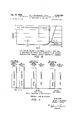
- FIGURE 1 is a top view of the heat sink and semiconductor means of the present invention.
- FIGURE 2 is a side view of the heat sink and semiconductor means of the invention shown in FIGURE 1.
- FIGURE 3 is an electrical schematic of the present invention cooperatively associated with cells of an electric storage battery.
- FIGURE 4 illustrates the current-voltage characteristic curve of the heat sink and semiconductor means with temperature feedback of the present invention compared to a semiconductor without temperature feedback.
- FIGURE 5 illustrates the typical percent loss in capacity of typical nickel-cadmium cells after cycling with and without the means and methods of the present invention.
- the means and methods of the present invention relates to an improved electrode regenerating device for rapid recharging of a single cell or a plurality of cells coupled in series.
- a heat sink and semiconductor means is coupled across the electrode terminals of a-second-ary cell in such a manner that the secondary cell is recharged rapidly without overcharge. If a plurality of series-coupled cells are to be recharged, a heat sink and semiconductor means is coupled across each of the plurality of cells.
- the present invention relates to a thermally isolated heat sink and diode means coupled so that heat feedback occurs.
- the heat feedback maintains a substantially constant forward voltage drop at a predetermined current value.
- the heat sink and diode means is coupled across the terminal electrodes of a cell to be recharged.
- the heat sink and diode means is substantially nonconductive when the voltage of the cell is below a predetermined voltage value and conductive when the cell is above the predetermined voltage value there'by recharging the secondary cell without overcharging thereof.
- the heat sink and semiconductor means is generally indicated by numeral 10.
- a wafer 11 of suitable semiconductor material such as silicon or germanium or the like, is disposed in the approximate center of heat sink 12 with a major surface thereof electrically connected to and securely held by the heat sink by any suitable bonding means such as sold-er or the like.
- the heat sink is fabricated from any suitable heat conductive metal such as anodized aluminum or the like.
- a braided copper shield wire 13 is attached to and extends from the other major surface of the Wafer thereby forming a rectifying junction.
- the heat sink is tightly coupled to mounting head 14.
- the head may be fabricated from any suitable metal such as aluminum or the like and may 'be plated with a noble metal to substantially prevent corrosion.
- a housing 15 includes a plurality of side walls 16 fixedly coupled at one end to the heat sink.
- the side walls are fabricated from any suitable metal such as copper or the like.
- the braided copper wire is suitably bonded and sealed to the side walls approximately equal distance from each side wall by any suitable electrically insulative material such as epoxy or the like.
- the epoxy serves to insulate the braided copper wire from the head and the side walls of the housing.
- FIGURE 3 shows a plurality of series-coupled cells 17, 18 and 19 coupled in series to a suitable power supply 20.
- the power supply may be a direct current source. Coupled in shunt with cell 17 is a heat sink and semiconductor means .10. Likewise, a heat sink and semiconductor means 10 is coupled in shunt with cell 18 and a heat sink and semiconductor means 10" is coupled in shunt with cell 19.
- a three position switch means 21 is coupled in series with the series connected cells so that the cells may be recharged when the switch is connected to terminal 22 or provide electrical current to activate load 23 when the switch is coupled to terminal 24. When the switch is coupled to terminal 23, charging current flows from the power supply in the direction of the arrow to the positive side of the secondary cells. When 'the cell voltage rises above a predetermined value, the heat sink and semiconductor means coupled across that cell becomes conductive and shunts the charging current around that cell preventing overcharge.
- the diode used and described in the US. Patent No. 3,148,322 shows approximately zero current up to a specified terminal voltage of about 1.3 volts. Above this point the diode draws progressively larger amounts of current as the voltage increases. When the voltage value reaches that of the clamping voltage, in this case approximately 1.5 volts, the impedance of the diode can be seen to pass through zero and becomes negative.
- the cell voltage triggers the cooperatively associated heat sink and semiconductor means to conduction, thereby providing a shunt path around the associated cell thus preventing overcharging of the cell.
- the heat sink and semiconductor means draws only a slight amount of current until the cell reaches a charged condition at which point the heat sink and semiconductor means passes substantially immediately into a state wherein its dynamic impedance is substantially zero. It is seen that the heat sink and semiconductor means immediately above the breakdown voltage passes through a region of zero impedance and becomes negative as contrasted with the relatively higher dynamic impedance of the semiconductor without a heat sink.
- the heat sink is thermally isolated from the cell and provides a thermal feedback loop to the diode.
- the forward voltage drop of the means is significantly reduced through use of the heating effect. It is seen that the heat sink provides a temperature feedback path to maintain a constant forward voltage drop over the operating current range. The heating effect becomes important only after the cell voltage approaches the terminal voltage. No significant increase in leakage current at voltages lower than the breakdown voltage of the present invention is noted.
- FIGURE 5 illustrates that the present invention will substantially prolong cell cycle life.
- Cycle tests wherein a first plurality of 1.2 ah. nickel-cadmium cells recharged in accordance with the present invention were subjected to'a 2-hour charge cycle and a 38 minute discharge at 0.5 ampere.
- a second plurality of 1.2 ah. nickel-cadmium cells were recharged using the 2-hour time cycle and a 38 minute discharge at 0.5 ampere but were not shunted by the means and method of the present invention.
- Results showed that the first plurality of nickel-cadmium cells recharged using the heat sink and semiconductor means exhibited a capacity loss of 3% after 345 cycles whereas the nickel-cadmium cells recharged without the heat sink and semiconductor means of the present invention showed a 100% loss in capacity after 345 cycles. After 615 cycles, the nickel-cadmium cells using the heat sink and semiconductor means showed a loss of about 7% whereas the unprotected cells showed a loss of 100%.
- a rechargeable cell and an electrode regeneration device connected in circiut together, said electrode regeneration device comprising heat sink and semiconductor means having at least two terminals and at least one junction mounted on said sink in heat exchange contact therewith, electrical conductors connecting said terminals of said heat sink and semiconductor means across said cell, said heat sink having thermal resistance which is such that the junction temperature of said semiconductor i such a function of the power dissipation of said semiconductor so as to maintain the junction voltage substantially constant and independent of current thereby bypassing currents above a specified rating around said cell.
- a plurality of rechargeable cells connected in series and an electrode regeneration device connected in circuit together
- said electrode regeneration device comprising a plurality of heat sink and semiconductor means, each of said heat sink and semiconductor means having at least two terminals and at least One junction mounted on said sink in heat exchange contact therewith, electrical conductors connecting said terminals of said heat sink and semiconductor means respectively across said cells, said heat sink having a thermal resistance which is such that the junction temperature of said semiconductor is such a function of the power dissipation of said semiconductor so as to maintain the junction voltage substantially constant and independent of current thereby bypassing currents above a specified rating around said cell.
- a rechargeable battery cell and an electrode regeneration device connected in circuit together, said electrode regeneration device comprising heat sink and diode means having at least two terminals and at least one junction mounted on said sink in heat exchange contact therewith, electrical conductors connecting said terminals of said heat sink and diode means across said cell, said heat sink having a thermal resistance which is such that the junction temperature of said diode is such a function of the power dissipation of said diode so as to maintain the junction voltage substantially constant and independent of current thereby bypassing currents above a specified rating around said cell.
- a plurality of rechargeable cells connected in series and an electrode regeneration device connected in circuit together
- said electrode regeneration device comprising a plurality of heat sink and diode means, each of said heat sink and diode means having at least two terminals and at least one junction mounted on said sink in heat exchange contact therewith, electrical conductors connecting said terminals of said heat sink and diode means respectively across said cells, said heat sink having a thermal resistance which is such that the junction temperature of said diode is such a function of the power dissipation of said diode so as to maintain the junction voltage substantially constant and independent of current thereby bypassing currents above a specified rating around said cell.
- a plurality of rechargeable cells connected in series and an electrode regeneration device connected in circuit together, said electrode regeneration device comprising a plurality of heat sink and diode means, each of said diode means having at least two terminals and at least one junction mounted on said sink in heat exchange contact therewith, electrical conductors connecting said terminals of said diode means respectively across said cells, said heat sink having a thermal resistance which is such that the junction temperature of said diode means is such a function of the power dissipation of said diode means so as to maintain the junction voltage substantially constant and independent of current thereby bypassing currents above a specified rating around said cell.
- a plurality of rechargeable cells connected in series thereby forming a battery means and an electrode regeneration device connected in circuit together
- said electrode regeneration device comprising a plurality of heat sink and diode means thermally isolated from said cells of said battery means, each of said diode means having at least two terminals and at least one junction mounted on said sink in heat exchange contact therewith, electrical conductors connecting said terminals of said diode means respectively across said cells, said heat sink having a thermal resistance which is such that the junction temperature of said diode means is such a function of the power dissipation of said diode means so as to maintain the junction voltage substantially constant and independent of current thereby bypassing currents above a specified rating around said cell.
- a plurality of rechargeable cells connected in series thereby forming a battery means and an electrode regeneration device connected in circuit together
- said electrode regeneration device comprising a plurality of anodized aluminum heat sink and diode means thermally isolated from said cells of said battery means, each of said diode means having at least two terminals and at least one junction mounted on said sink in heat exchange contact therewith, electrical conductors connecting said terminals of said diode means respectively across said cells, said heat sink having a thermal resistance which is such that the junction temperature of said diode means is such a function of the power dissipation of said diode means so as to maintain the junction voltage substantially constant and independent of current thereby bypassing currents above a specified rating around said cell.
- said electrode regeneration device comprising a plurality of anodized aluminum heat sink and diode means thermally isolated from said cells of said battery means, each of said diode means having at least two terminals and at least one junction mounted on said sink in heat exchange contact therewith, an electrical conductor connecting said terminal of said diode means respectively across said cells, said heat sink having a thermal resistance which is such that the junction te'm ing said cells to said electrode'regeneration device 'or a" load.
Landscapes
- Engineering & Computer Science (AREA)
- Power Engineering (AREA)
- Chemical & Material Sciences (AREA)
- General Physics & Mathematics (AREA)
- Physics & Mathematics (AREA)
- Condensed Matter Physics & Semiconductors (AREA)
- Materials Engineering (AREA)
- Computer Hardware Design (AREA)
- Microelectronics & Electronic Packaging (AREA)
- Manufacturing & Machinery (AREA)
- Chemical Kinetics & Catalysis (AREA)
- Electrochemistry (AREA)
- General Chemical & Material Sciences (AREA)
- Charge And Discharge Circuits For Batteries Or The Like (AREA)
- Secondary Cells (AREA)
Description
y 1968 P. J. WHORISKEY ETAL ,3
SEMICONDUCTOR CHARGE CONTROL THROUGH THERMAL ISOLATION OF SEMICONDUCTOR AND CELL Filed Aug- 9, 1965 2 Sheets-Sheet 1 CHARGE CURRENT IO OVER CHARGE CURRENT & J POWER 22 SUPPLY LOAD 23 l9 l0& I
PETER J. WHOR/SKE Y FRANK J. COCCA ATTORNEY 3,393,355 SOLATION 2 Sheets-Sheet UN- PROTECTED CELLS AFTER INVE/V 70/?5 ATTORN Y 615 CYCLES PETER J. WHOR/SKE Y FRANK J. COCCA P. J. WHORISKEY ETAL OF SEMICONDUCTOR AND CELL AFTER 345 CYCLES SEMICONDUCTOR CHARGE C(NTROL THROUGH THERMAL I led Aug. 9, 196
CYCLING coumzacm. L2 AH m-co. CELLS PERCENT LOSS IN CAPACITY Y K R C K s mm M N w R M- M O "H. m D M EN 0 w M H A E m m r o n u \omm E A W SWMTE m T m m w R A M P OD R HE F m a s S M M m M w E S O m M m C W as R w m m 4 r m 553 $0 0 S C m T oc !N U M D M W A s R m m mmH mm w E m USTS 0 E M M mmmu o n o \ohm nlbl G OE E M M R M.. ACMOC O E I R E 0.0 m P 3 VW R s a 5 E m K O R N C W E 0 W s P l N D M T A M o w A PC .68 c E E M Mn t0 m o \oOO H ma uom H R T P m m G Kc N 4 3 2 I MWSHS 0 Human to m o \oOO $51.5 umumu M R H P 8 July 16, 1968 NEW CELLS United States Patent 3,393,355 SEMICONDUCTOR CHARGE CONTROL THROUGH THERMAL ISOLATION OF SEMICONDUCTOR AND CELL Peter J. Whorislrey, Winchester, and Frank J. Cocca, East Boston, Mass, assignors to P. R. Mallory & Co. Inc., Indianapolis, Ind., a corporation of Delaware Filed Aug. 9, 1965, Ser. No. 478,324 8 Claims. (Cl. 320-48) ABSTRACT OF THE DISCLOSURE A heat sink and semiconductor means connected across a battery cell to be charged wherein the heat sink has a thermal resistance which is such that the junction temperature of the semiconductor is such a function of the power dissipation of the semiconductor so as to maintain the junction voltage substantially constant and independent of current.
The present invention relates, generally, to rechargeable electric means, more particularly, to means and methods for rapid charging thereof without deleterious eflects.
An efiicient, simple, and effective means of preventing overcharging of a secondary cell has been sought for many years. It is known that recharging of the secondary cells may be accomplished by reconstituting the electrodes of the cell. However, a means of accurately terminating the recharging cycle of the secondary cell when the cell attains its full recharged state has eluded those skilled in the art.
During the initial phases of a recharge cycle of a secondary cell, it is known that substantially all the electrical energy is converted into chemical energy, thereby evolving no heat or an insignificant amount of heat that has substantially no harmful effect on the secondary cell. As the secondary cell is recharged, oxygen is evolved at one of the electrodes of the cell and thereafter chemically reduced at the other electrode of the cell. The aforementioned chemical reduction of the oxygen is continuous until such time as the secondary cell has its electrodes fully reconstituted. When the electrodes are reconstituted, the cell has attained its so-called fully recharged state. Continued recharging of the secondary cell at rates in excess of the equilibrium charge rates has resulted in the creation of harmful conditions. It is known that a fully recharged secondary cell may not reduce the oxygen evolved at the same rate at which it is evolved Therefore, if the overcharging period is continued at a rate in excess of the equilibrium charge rate, the electrodes of the secondary cell can be damaged and, if the cell is hermetically sealed, pressure substantially increases within the cell due to the accumulation of oxygen. Prolonged subjection to an overcharging period may rupture and/ or explode the cell.
In addition to the oxygen accumulation causing a significant increase in the internal pressure of the cell, and the damage suffered by the electrodes, harmful heat is generated within the cell since the conversion of elect-rical energy to chemical energy has substantially terminated. It is seen that overrecharging not only increases the internal pressure contained within the cell but reduces the effectiveness of the electrodes and also evolves heat Which causes the voltage of the cell to fall. On the other hand, if the voltage of the cell rises above a predetermined value, hydrogen gas is evolved which, it is thought will not recombine within the cell.
The maximum continuous overcharging current to which a secondary cell may be subjected for extended periods of time has been established by industry. Recharging at the aforementioned established rate establishes a so-called equilibrium condition whereby the rate of evolution of oxygen at one electrode of the cell is equal to the rate of reduction of the evolved oxygen at the other electrode of the cell. This charging level is referred to as the C/ 10 rate for nickel-cadmium cells, wherein C is normal capacity of the secondary cell. It is seen that for a 1.25 ah. nickel-cadmium cell, that C/10=0.125 ampere. Silver-cadmium cells have an equilibrium charging rate of approximately C/ and other types of cells may have other equilibrium rates.
The acceptance of the so-called cordless appliance is becoming more widespread. The cordless appliance uses, as a source of electrical energy, a rechargeable electric battery. It has been found that the user of the battery cannot be expected to accurately terminate the charging cycle after a specified time to avoid overcharging the plurality of cells of the battery. Also, there is no simple method that can be utilized to ascertain the remaining charge left in the cells of a used battery, the C/ 10 rates of recharge is the maximum safe rate of equilibrium recharging accepted by industry to recharge a nickel-cadmium battery. As a general rule, the C/ 10 rate of recharge requires from 14 to 16 hours to reconstitute the electrodes of nickel-cadimum cells.
The means and method of the present invention allow each cell of the battery to be recharged at a much faster rate yet prevent the cell from being overcharged by shunting substantially all of the charging current around the cooperatively associated secondary cell at or immediately prior to the associated secondary cell attaining its fully recharged state. The means and methods of the present invention shunt substantially all the current produced by the charging source of electrical energy except for an equilibrium current which is allowed to tricklecharge a cell after the electrodes of the cell have been reconstituted. Each of the plurality of cells forming the battery is provided with its own means of the present invention so that each cell may be fully reconstituted independent of the initial state of charge of the other cells of the battery and so that slight electrochemical variations between the several cells may be taken into consideration. By using the means and methods of the present invention, recharging time durations in the order of 2 to 3 hours may be achieved as compared to the 14 to 16 hours required by several of the prior art devices.
The means and method of the present invention act as a voltage sensitive gate means to shunt the recharging current around the cell when the cell attains a predetermined recharge state. A specially designed heat sink is utilized to allow the semiconductor means of the present invention to take advantage of the semiconductor means negative temperature coefficient. By utilizing a heat sink of a specific design, the current-voltage is made to exhibit a thermally induced negative resistance region. Therefore, the heat sink is a calibrated heat dissipator. As a result, the combination of the heat sink and semiconductor means permits the diode to shunt a progressively larger share of the charging current around the cooperatively associated cell than would otherwise be possible when the cell voltage reaches a predetermined voltage.
Therefore, it is an object of the present invention to provide a heat sink and semiconductor means cooperat-ively associated with an electrical storage battery to prevent overcharging of the battery.
It is another object of the present invention to provide a heat sink and semi-conductor means cooperatively associated with each of the plurality of cells of an electrical battery so as to effectively terminate the recharge of each cell when the individual cell attains a predetermined recharged condition.
Another object of the present invention is to provide a novel heat sink and semiconductor means cooperatively associated with a plurality of secondary electrical cells that acts as a voltage-sensitive gate means to shunt a charging current around the secondary electrical cells when the cells reach a predetermied recharged state.
Still another object of the present invention is to provide a heat sink and semiconductor means cooperatively associated with a rechargeable battery means which is of sturdy construction and so composed as to be a selfcontained device that is characterized by its accuracy of operation.
Yet still another object of the present invention is to provide a heat sink and semiconductor means cooperatively associated with a rechargeable battery means that is efficient, inexpensive, simple, accurate and effective in operation.
A further object of the present invention is to provide a heat sink and semiconductor means used with a rechargeable battery means that makes use of the semiconductors voltage temperature coefficient to all-ow the semiconductor means to more accurately control the recharging cycle of the rechargeable battery means.
Another object of the present invention is to provide a heat sink and semiconductor means used with a rechargeable electrical storage battery means having a plurality of serially connected cells wherein the semiconductor is thermally isolated from the cells of the battery means.
Yet another object of the present invention is to provide combination heat sink and semiconductor means cooperatively associated with a plurality 'of rechargeable electric cells wherein the recharge cycle of said cells may be accomplished within 2 to 3 hours.
A further object of the present invention is to provide a combination heat sink and semiconductor means wherein the semiconductor characteristics are enhanced by the use of the heat sink which provides a temperature feedback path to maintain a constant forward voltage drop over an operating current range.
The present invention, in another of its aspects, relates to novel features of the instrumentalities described herein for teaching the principal object of the invention and to the novel principles employed in the instrumentalities whether or not these features and principles may be used in the said object and/or in the said field.
With the aforementioned objects enumerated, other objects will be apparent to those persons possessing ordinary skill in the art. Also other objects will appear in the following description, appended claims, and appended drawings. The invention resides in the novel construction, combination, arrangement, and cooperation of elements as hereinafter described and more particularly as defined in the appended claims.
' The appended drawings illustrate the present invention constructed to function for the practical application of the basic principles involved in the hereinafter described invention.
In the drawings:
FIGURE 1 is a top view of the heat sink and semiconductor means of the present invention.
FIGURE 2 is a side view of the heat sink and semiconductor means of the invention shown in FIGURE 1.
FIGURE 3 is an electrical schematic of the present invention cooperatively associated with cells of an electric storage battery.
FIGURE 4 illustrates the current-voltage characteristic curve of the heat sink and semiconductor means with temperature feedback of the present invention compared to a semiconductor without temperature feedback.
FIGURE 5 illustrates the typical percent loss in capacity of typical nickel-cadmium cells after cycling with and without the means and methods of the present invention.
Generally speaking, the means and methods of the present invention relates to an improved electrode regenerating device for rapid recharging of a single cell or a plurality of cells coupled in series. A heat sink and semiconductor means is coupled across the electrode terminals of a-second-ary cell in such a manner that the secondary cell is recharged rapidly without overcharge. If a plurality of series-coupled cells are to be recharged, a heat sink and semiconductor means is coupled across each of the plurality of cells.
More particularly, the present invention relates to a thermally isolated heat sink and diode means coupled so that heat feedback occurs. The heat feedback maintains a substantially constant forward voltage drop at a predetermined current value. The heat sink and diode means is coupled across the terminal electrodes of a cell to be recharged. The heat sink and diode means is substantially nonconductive when the voltage of the cell is below a predetermined voltage value and conductive when the cell is above the predetermined voltage value there'by recharging the secondary cell without overcharging thereof.
Referring now to the drawings, which illustrate an embodiment of the present invention, the heat sink and semiconductor means is generally indicated by numeral 10. A wafer 11 of suitable semiconductor material, such as silicon or germanium or the like, is disposed in the approximate center of heat sink 12 with a major surface thereof electrically connected to and securely held by the heat sink by any suitable bonding means such as sold-er or the like. The heat sink is fabricated from any suitable heat conductive metal such as anodized aluminum or the like. A braided copper shield wire 13 is attached to and extends from the other major surface of the Wafer thereby forming a rectifying junction. The heat sink is tightly coupled to mounting head 14. The head may be fabricated from any suitable metal such as aluminum or the like and may 'be plated with a noble metal to substantially prevent corrosion.
A housing 15 includes a plurality of side walls 16 fixedly coupled at one end to the heat sink. The side walls are fabricated from any suitable metal such as copper or the like. The braided copper wire is suitably bonded and sealed to the side walls approximately equal distance from each side wall by any suitable electrically insulative material such as epoxy or the like. The epoxy serves to insulate the braided copper wire from the head and the side walls of the housing.
U.S. Patent No. 3,148,322, assigned to P. R. Mallory Co. Inc., the assignee of the present invention, shows the electrical schematic shown and illustrated in FIGURE 3. The voltage sensitive means described andillustrated in the aforementioned patent have had substituted therefor the novel heat sink and semiconductor means of the present invention.
Briefly, FIGURE 3 shows a plurality of series-coupled cells 17, 18 and 19 coupled in series to a suitable power supply 20. The power supply may be a direct current source. Coupled in shunt with cell 17 is a heat sink and semiconductor means .10. Likewise, a heat sink and semiconductor means 10 is coupled in shunt with cell 18 and a heat sink and semiconductor means 10" is coupled in shunt with cell 19. A three position switch means 21 is coupled in series with the series connected cells so that the cells may be recharged when the switch is connected to terminal 22 or provide electrical current to activate load 23 when the switch is coupled to terminal 24. When the switch is coupled to terminal 23, charging current flows from the power supply in the direction of the arrow to the positive side of the secondary cells. When 'the cell voltage rises above a predetermined value, the heat sink and semiconductor means coupled across that cell becomes conductive and shunts the charging current around that cell preventing overcharge.
As shown in FIGURE 4, the diode used and described in the US. Patent No. 3,148,322 shows approximately zero current up to a specified terminal voltage of about 1.3 volts. Above this point the diode draws progressively larger amounts of current as the voltage increases. When the voltage value reaches that of the clamping voltage, in this case approximately 1.5 volts, the impedance of the diode can be seen to pass through zero and becomes negative.
As shown in FIGURE 4, when the cell with the particular heat sink and semiconductor means reaches its predetermined fully recharged condition, the cell voltage triggers the cooperatively associated heat sink and semiconductor means to conduction, thereby providing a shunt path around the associated cell thus preventing overcharging of the cell. It is seen that the heat sink and semiconductor means draws only a slight amount of current until the cell reaches a charged condition at which point the heat sink and semiconductor means passes substantially immediately into a state wherein its dynamic impedance is substantially zero. It is seen that the heat sink and semiconductor means immediately above the breakdown voltage passes through a region of zero impedance and becomes negative as contrasted with the relatively higher dynamic impedance of the semiconductor without a heat sink.
As indicated hereinbefore, the heat sink is thermally isolated from the cell and provides a thermal feedback loop to the diode. The forward voltage drop of the means is significantly reduced through use of the heating effect. It is seen that the heat sink provides a temperature feedback path to maintain a constant forward voltage drop over the operating current range. The heating effect becomes important only after the cell voltage approaches the terminal voltage. No significant increase in leakage current at voltages lower than the breakdown voltage of the present invention is noted.
FIGURE 5 illustrates that the present invention will substantially prolong cell cycle life. Cycle tests wherein a first plurality of 1.2 ah. nickel-cadmium cells recharged in accordance with the present invention were subjected to'a 2-hour charge cycle and a 38 minute discharge at 0.5 ampere. A second plurality of 1.2 ah. nickel-cadmium cells were recharged using the 2-hour time cycle and a 38 minute discharge at 0.5 ampere but were not shunted by the means and method of the present invention. Results showed that the first plurality of nickel-cadmium cells recharged using the heat sink and semiconductor means exhibited a capacity loss of 3% after 345 cycles whereas the nickel-cadmium cells recharged without the heat sink and semiconductor means of the present invention showed a 100% loss in capacity after 345 cycles. After 615 cycles, the nickel-cadmium cells using the heat sink and semiconductor means showed a loss of about 7% whereas the unprotected cells showed a loss of 100%.
While the invention is described and illustrated with reference to a specific means and method, it will be understood that modifications and variations may be effected without departing from the scope of the novel concepts of this invention and as set forth in the appended claims.
Having thus described our invention, we claim:
1. In combination, a rechargeable cell and an electrode regeneration device connected in circiut together, said electrode regeneration device comprising heat sink and semiconductor means having at least two terminals and at least one junction mounted on said sink in heat exchange contact therewith, electrical conductors connecting said terminals of said heat sink and semiconductor means across said cell, said heat sink having thermal resistance which is such that the junction temperature of said semiconductor i such a function of the power dissipation of said semiconductor so as to maintain the junction voltage substantially constant and independent of current thereby bypassing currents above a specified rating around said cell.
2. In combination, a plurality of rechargeable cells connected in series and an electrode regeneration device connected in circuit together, said electrode regeneration device comprising a plurality of heat sink and semiconductor means, each of said heat sink and semiconductor means having at least two terminals and at least One junction mounted on said sink in heat exchange contact therewith, electrical conductors connecting said terminals of said heat sink and semiconductor means respectively across said cells, said heat sink having a thermal resistance which is such that the junction temperature of said semiconductor is such a function of the power dissipation of said semiconductor so as to maintain the junction voltage substantially constant and independent of current thereby bypassing currents above a specified rating around said cell.
3. In combination, a rechargeable battery cell and an electrode regeneration device connected in circuit together, said electrode regeneration device comprising heat sink and diode means having at least two terminals and at least one junction mounted on said sink in heat exchange contact therewith, electrical conductors connecting said terminals of said heat sink and diode means across said cell, said heat sink having a thermal resistance which is such that the junction temperature of said diode is such a function of the power dissipation of said diode so as to maintain the junction voltage substantially constant and independent of current thereby bypassing currents above a specified rating around said cell.
4. In combination, a plurality of rechargeable cells connected in series and an electrode regeneration device connected in circuit together, said electrode regeneration device comprising a plurality of heat sink and diode means, each of said heat sink and diode means having at least two terminals and at least one junction mounted on said sink in heat exchange contact therewith, electrical conductors connecting said terminals of said heat sink and diode means respectively across said cells, said heat sink having a thermal resistance which is such that the junction temperature of said diode is such a function of the power dissipation of said diode so as to maintain the junction voltage substantially constant and independent of current thereby bypassing currents above a specified rating around said cell.
5. In combination, a plurality of rechargeable cells connected in series and an electrode regeneration device connected in circuit together, said electrode regeneration device comprising a plurality of heat sink and diode means, each of said diode means having at least two terminals and at least one junction mounted on said sink in heat exchange contact therewith, electrical conductors connecting said terminals of said diode means respectively across said cells, said heat sink having a thermal resistance which is such that the junction temperature of said diode means is such a function of the power dissipation of said diode means so as to maintain the junction voltage substantially constant and independent of current thereby bypassing currents above a specified rating around said cell.
6. In combination, a plurality of rechargeable cells connected in series thereby forming a battery means and an electrode regeneration device connected in circuit together, said electrode regeneration device comprising a plurality of heat sink and diode means thermally isolated from said cells of said battery means, each of said diode means having at least two terminals and at least one junction mounted on said sink in heat exchange contact therewith, electrical conductors connecting said terminals of said diode means respectively across said cells, said heat sink having a thermal resistance which is such that the junction temperature of said diode means is such a function of the power dissipation of said diode means so as to maintain the junction voltage substantially constant and independent of current thereby bypassing currents above a specified rating around said cell.
7. In combination, a plurality of rechargeable cells connected in series thereby forming a battery means and an electrode regeneration device connected in circuit together, said electrode regeneration device comprising a plurality of anodized aluminum heat sink and diode means thermally isolated from said cells of said battery means, each of said diode means having at least two terminals and at least one junction mounted on said sink in heat exchange contact therewith, electrical conductors connecting said terminals of said diode means respectively across said cells, said heat sink having a thermal resistance which is such that the junction temperature of said diode means is such a function of the power dissipation of said diode means so as to maintain the junction voltage substantially constant and independent of current thereby bypassing currents above a specified rating around said cell.
8. In combination, a plurality of rechargeable battery cells connected in series thereby forming battery means and an electrode regeneration device and a switch means connected in circuit together, said electrode regeneration device comprising a plurality of anodized aluminum heat sink and diode means thermally isolated from said cells of said battery means, each of said diode means having at least two terminals and at least one junction mounted on said sink in heat exchange contact therewith, an electrical conductor connecting said terminal of said diode means respectively across said cells, said heat sink having a thermal resistance which is such that the junction te'm ing said cells to said electrode'regeneration device 'or a" load.
References Cited UNITED STATES PATENTS 2,827,597 3/1958 Lidow 317-234 2,471,011 5/1949 Shapiro 317-234X 2,624,033 12/1952 Jacquier -320.53; 2,994,017 7/ 1961 Kadelburg; -31-7--23-,4 3,148,322 9/1964 Booe' vetzal. 320-,43 3,217,213, 11/1965 Slater 317234:, 3,265,805 8/1966 Carlan et al. 1,74,15.X
OTHER REFERENCES Motorola, Silicon Zener Diode and Rectifier 1961, pp. 119420.
LEE T. HIX, Primary Examiner.
WARREN E. RAY, Examiner.
S. WEINBERG, Assistant Examiner";
Priority Applications (4)
| Application Number | Priority Date | Filing Date | Title |
|---|---|---|---|
| US478324A US3393355A (en) | 1965-08-09 | 1965-08-09 | Semiconductor charge control through thermal isolation of semiconductor and cell |
| GB33035/66A GB1152195A (en) | 1965-08-09 | 1966-07-22 | Arrangement for Recharging Electric Cells |
| NL6610962A NL6610962A (en) | 1965-08-09 | 1966-08-04 | |
| DE19661563564 DE1563564C (en) | 1965-08-09 | 1966-08-05 | Overcharge protection device for a rechargeable electrical collector cell |
Applications Claiming Priority (1)
| Application Number | Priority Date | Filing Date | Title |
|---|---|---|---|
| US478324A US3393355A (en) | 1965-08-09 | 1965-08-09 | Semiconductor charge control through thermal isolation of semiconductor and cell |
Publications (1)
| Publication Number | Publication Date |
|---|---|
| US3393355A true US3393355A (en) | 1968-07-16 |
Family
ID=23899464
Family Applications (1)
| Application Number | Title | Priority Date | Filing Date |
|---|---|---|---|
| US478324A Expired - Lifetime US3393355A (en) | 1965-08-09 | 1965-08-09 | Semiconductor charge control through thermal isolation of semiconductor and cell |
Country Status (3)
| Country | Link |
|---|---|
| US (1) | US3393355A (en) |
| GB (1) | GB1152195A (en) |
| NL (1) | NL6610962A (en) |
Cited By (34)
| Publication number | Priority date | Publication date | Assignee | Title |
|---|---|---|---|---|
| US4303877A (en) * | 1978-05-05 | 1981-12-01 | Brown, Boveri & Cie Aktiengesellschaft | Circuit for protecting storage cells |
| US4311952A (en) * | 1973-11-02 | 1982-01-19 | Mabuchi Motor Co. Ltd. | Battery charging system |
| US4349773A (en) * | 1979-12-04 | 1982-09-14 | Brown, Boveri & Cie Aktiengesellschaft | Circuit for protecting storage cells |
| US4713597A (en) * | 1985-12-04 | 1987-12-15 | Powerplex Technologies, Inc. | Silicon diode looping element for protecting a battery cell |
| US4719401A (en) * | 1985-12-04 | 1988-01-12 | Powerplex Technologies, Inc. | Zener diode looping element for protecting a battery cell |
| US5063340A (en) * | 1990-10-25 | 1991-11-05 | Motorola, Inc. | Capacitive power supply having charge equalization circuit |
| WO1999004476A1 (en) * | 1997-07-14 | 1999-01-28 | Johnson Lonnie G | Rechargeable battery power supply overcharge protection circuit |
| US6242129B1 (en) | 1999-04-02 | 2001-06-05 | Excellatron Solid State, Llc | Thin lithium film battery |
| US6387563B1 (en) | 2000-03-28 | 2002-05-14 | Johnson Research & Development, Inc. | Method of producing a thin film battery having a protective packaging |
| US6398824B1 (en) | 1999-04-02 | 2002-06-04 | Excellatron Solid State, Llc | Method for manufacturing a thin-film lithium battery by direct deposition of battery components on opposite sides of a current collector |
| US6402796B1 (en) | 2000-08-07 | 2002-06-11 | Excellatron Solid State, Llc | Method of producing a thin film battery |
| US6423106B1 (en) | 2000-04-05 | 2002-07-23 | Johnson Research & Development | Method of producing a thin film battery anode |
| US20020110733A1 (en) * | 2000-08-07 | 2002-08-15 | Johnson Lonnie G. | Systems and methods for producing multilayer thin film energy storage devices |
| US6511516B1 (en) | 2000-02-23 | 2003-01-28 | Johnson Research & Development Co., Inc. | Method and apparatus for producing lithium based cathodes |
| US6582481B1 (en) | 1999-11-23 | 2003-06-24 | Johnson Research & Development Company, Inc. | Method of producing lithium base cathodes |
| US20050008772A1 (en) * | 2003-07-11 | 2005-01-13 | Ji-Guang Zhang | System and method of producing thin-film electrolyte |
| US20050016458A1 (en) * | 2003-07-11 | 2005-01-27 | Ji-Guang Zhang | Apparatus for producing thin-film electrolyte |
| US20050208353A1 (en) * | 2004-02-20 | 2005-09-22 | Johnson Lonnie G | Lithium oxygen batteries and method of producing same |
| US20070099078A1 (en) * | 2002-01-10 | 2007-05-03 | Ji-Guang Zhang | Packaged thin film batteries and methods of packaging thin film batteries |
| US20070094865A1 (en) * | 2002-01-10 | 2007-05-03 | Ji-Guang Zhang | Packaged thin film batteries and methods of packaging thin film batteries |
| US20080070087A1 (en) * | 2004-02-20 | 2008-03-20 | Excellatron Solid State, Llc | Non-volatile cathodes for lithium oxygen batteries and method of producing same |
| US20090004371A1 (en) * | 2007-06-29 | 2009-01-01 | Johnson Lonnie G | Amorphous lithium lanthanum titanate thin films manufacturing method |
| US20090092903A1 (en) * | 2007-08-29 | 2009-04-09 | Johnson Lonnie G | Low Cost Solid State Rechargeable Battery and Method of Manufacturing Same |
| US20090098281A1 (en) * | 2005-10-11 | 2009-04-16 | Ji-Guang Zhang | Method of manufacturing lithium battery |
| US20090239132A1 (en) * | 2008-03-20 | 2009-09-24 | Excellatron Solid State, Llc | Oxygen battery system |
| US7731765B2 (en) | 2004-02-20 | 2010-06-08 | Excellatron Solid State, Llc | Air battery and manufacturing method |
| US20110053001A1 (en) * | 2008-06-27 | 2011-03-03 | Excellatron Solid State Llc | Ionically-conductive amorphous lithium lanthanum zirconium oxide |
| US8568921B1 (en) | 2004-08-18 | 2013-10-29 | Excellatron Solid State Llc | Regenerative ion exchange fuel cell |
| US9356317B2 (en) | 2007-06-29 | 2016-05-31 | Johnson Ip Holding, Llc | Amorphous ionically conductive metal oxides and sol gel method of preparation |
| US9793525B2 (en) | 2012-10-09 | 2017-10-17 | Johnson Battery Technologies, Inc. | Solid-state battery electrodes |
| US10218044B2 (en) | 2016-01-22 | 2019-02-26 | Johnson Ip Holding, Llc | Johnson lithium oxygen electrochemical engine |
| US10333123B2 (en) | 2012-03-01 | 2019-06-25 | Johnson Ip Holding, Llc | High capacity solid state composite cathode, solid state composite separator, solid-state rechargeable lithium battery and methods of making same |
| US10566669B2 (en) | 2004-02-20 | 2020-02-18 | Johnson Ip Holding, Llc | Lithium oxygen batteries having a carbon cloth current collector and method of producing same |
| US10566611B2 (en) | 2015-12-21 | 2020-02-18 | Johnson Ip Holding, Llc | Solid-state batteries, separators, electrodes, and methods of fabrication |
Families Citing this family (1)
| Publication number | Priority date | Publication date | Assignee | Title |
|---|---|---|---|---|
| GB2189951A (en) * | 1986-04-30 | 1987-11-04 | Lilliwyte Sa | Charging electrochemical storage cells |
Citations (7)
| Publication number | Priority date | Publication date | Assignee | Title |
|---|---|---|---|---|
| US2471011A (en) * | 1946-12-19 | 1949-05-24 | Arthur L Shapiro | Battery charger and rectifier therefor |
| US2624033A (en) * | 1950-09-11 | 1952-12-30 | Accumulateurs Fixes & De Tract | Series connected cells with individual rectifier shunts |
| US2827597A (en) * | 1953-10-02 | 1958-03-18 | Int Rectifier Corp | Rectifying mounting |
| US2994017A (en) * | 1956-09-07 | 1961-07-25 | Int Rectifier Corp | Air-cooled rectifier assembly |
| US3148322A (en) * | 1961-03-13 | 1964-09-08 | Mallory & Co Inc P R | Rechargeable battery with means to prevent overcharging |
| US3217213A (en) * | 1961-06-02 | 1965-11-09 | Slater Electric Inc | Semiconductor diode construction with heat dissipating housing |
| US3265805A (en) * | 1964-02-03 | 1966-08-09 | Power Components Inc | Semiconductor power device |
-
1965
- 1965-08-09 US US478324A patent/US3393355A/en not_active Expired - Lifetime
-
1966
- 1966-07-22 GB GB33035/66A patent/GB1152195A/en not_active Expired
- 1966-08-04 NL NL6610962A patent/NL6610962A/xx unknown
Patent Citations (7)
| Publication number | Priority date | Publication date | Assignee | Title |
|---|---|---|---|---|
| US2471011A (en) * | 1946-12-19 | 1949-05-24 | Arthur L Shapiro | Battery charger and rectifier therefor |
| US2624033A (en) * | 1950-09-11 | 1952-12-30 | Accumulateurs Fixes & De Tract | Series connected cells with individual rectifier shunts |
| US2827597A (en) * | 1953-10-02 | 1958-03-18 | Int Rectifier Corp | Rectifying mounting |
| US2994017A (en) * | 1956-09-07 | 1961-07-25 | Int Rectifier Corp | Air-cooled rectifier assembly |
| US3148322A (en) * | 1961-03-13 | 1964-09-08 | Mallory & Co Inc P R | Rechargeable battery with means to prevent overcharging |
| US3217213A (en) * | 1961-06-02 | 1965-11-09 | Slater Electric Inc | Semiconductor diode construction with heat dissipating housing |
| US3265805A (en) * | 1964-02-03 | 1966-08-09 | Power Components Inc | Semiconductor power device |
Cited By (46)
| Publication number | Priority date | Publication date | Assignee | Title |
|---|---|---|---|---|
| US4311952A (en) * | 1973-11-02 | 1982-01-19 | Mabuchi Motor Co. Ltd. | Battery charging system |
| US4303877A (en) * | 1978-05-05 | 1981-12-01 | Brown, Boveri & Cie Aktiengesellschaft | Circuit for protecting storage cells |
| US4349773A (en) * | 1979-12-04 | 1982-09-14 | Brown, Boveri & Cie Aktiengesellschaft | Circuit for protecting storage cells |
| US4713597A (en) * | 1985-12-04 | 1987-12-15 | Powerplex Technologies, Inc. | Silicon diode looping element for protecting a battery cell |
| US4719401A (en) * | 1985-12-04 | 1988-01-12 | Powerplex Technologies, Inc. | Zener diode looping element for protecting a battery cell |
| US5063340A (en) * | 1990-10-25 | 1991-11-05 | Motorola, Inc. | Capacitive power supply having charge equalization circuit |
| WO1992008269A1 (en) * | 1990-10-25 | 1992-05-14 | Motorola, Inc. | Capacitive power supply having charge equalization circuit |
| US5982144A (en) * | 1997-07-14 | 1999-11-09 | Johnson Research & Development Company, Inc. | Rechargeable battery power supply overcharge protection circuit |
| WO1999004476A1 (en) * | 1997-07-14 | 1999-01-28 | Johnson Lonnie G | Rechargeable battery power supply overcharge protection circuit |
| US6242129B1 (en) | 1999-04-02 | 2001-06-05 | Excellatron Solid State, Llc | Thin lithium film battery |
| US6398824B1 (en) | 1999-04-02 | 2002-06-04 | Excellatron Solid State, Llc | Method for manufacturing a thin-film lithium battery by direct deposition of battery components on opposite sides of a current collector |
| US6582481B1 (en) | 1999-11-23 | 2003-06-24 | Johnson Research & Development Company, Inc. | Method of producing lithium base cathodes |
| US6511516B1 (en) | 2000-02-23 | 2003-01-28 | Johnson Research & Development Co., Inc. | Method and apparatus for producing lithium based cathodes |
| US6387563B1 (en) | 2000-03-28 | 2002-05-14 | Johnson Research & Development, Inc. | Method of producing a thin film battery having a protective packaging |
| US6423106B1 (en) | 2000-04-05 | 2002-07-23 | Johnson Research & Development | Method of producing a thin film battery anode |
| US6402796B1 (en) | 2000-08-07 | 2002-06-11 | Excellatron Solid State, Llc | Method of producing a thin film battery |
| US20020110733A1 (en) * | 2000-08-07 | 2002-08-15 | Johnson Lonnie G. | Systems and methods for producing multilayer thin film energy storage devices |
| US20070099078A1 (en) * | 2002-01-10 | 2007-05-03 | Ji-Guang Zhang | Packaged thin film batteries and methods of packaging thin film batteries |
| US7960054B2 (en) | 2002-01-10 | 2011-06-14 | Excellatron Solid State Llc | Packaged thin film batteries |
| US20070094865A1 (en) * | 2002-01-10 | 2007-05-03 | Ji-Guang Zhang | Packaged thin film batteries and methods of packaging thin film batteries |
| US20050016458A1 (en) * | 2003-07-11 | 2005-01-27 | Ji-Guang Zhang | Apparatus for producing thin-film electrolyte |
| US6852139B2 (en) | 2003-07-11 | 2005-02-08 | Excellatron Solid State, Llc | System and method of producing thin-film electrolyte |
| US6886240B2 (en) | 2003-07-11 | 2005-05-03 | Excellatron Solid State, Llc | Apparatus for producing thin-film electrolyte |
| US20050008772A1 (en) * | 2003-07-11 | 2005-01-13 | Ji-Guang Zhang | System and method of producing thin-film electrolyte |
| US7691536B2 (en) | 2004-02-20 | 2010-04-06 | Excellatron Solid State, Llc | Lithium oxygen batteries and method of producing same |
| US7731765B2 (en) | 2004-02-20 | 2010-06-08 | Excellatron Solid State, Llc | Air battery and manufacturing method |
| US20080070087A1 (en) * | 2004-02-20 | 2008-03-20 | Excellatron Solid State, Llc | Non-volatile cathodes for lithium oxygen batteries and method of producing same |
| US20050208353A1 (en) * | 2004-02-20 | 2005-09-22 | Johnson Lonnie G | Lithium oxygen batteries and method of producing same |
| US10566669B2 (en) | 2004-02-20 | 2020-02-18 | Johnson Ip Holding, Llc | Lithium oxygen batteries having a carbon cloth current collector and method of producing same |
| US8568921B1 (en) | 2004-08-18 | 2013-10-29 | Excellatron Solid State Llc | Regenerative ion exchange fuel cell |
| US20090098281A1 (en) * | 2005-10-11 | 2009-04-16 | Ji-Guang Zhang | Method of manufacturing lithium battery |
| US7540886B2 (en) | 2005-10-11 | 2009-06-02 | Excellatron Solid State, Llc | Method of manufacturing lithium battery |
| US20090004371A1 (en) * | 2007-06-29 | 2009-01-01 | Johnson Lonnie G | Amorphous lithium lanthanum titanate thin films manufacturing method |
| US9356317B2 (en) | 2007-06-29 | 2016-05-31 | Johnson Ip Holding, Llc | Amorphous ionically conductive metal oxides and sol gel method of preparation |
| US8211496B2 (en) | 2007-06-29 | 2012-07-03 | Johnson Ip Holding, Llc | Amorphous lithium lanthanum titanate thin films manufacturing method |
| US20090092903A1 (en) * | 2007-08-29 | 2009-04-09 | Johnson Lonnie G | Low Cost Solid State Rechargeable Battery and Method of Manufacturing Same |
| US20090239132A1 (en) * | 2008-03-20 | 2009-09-24 | Excellatron Solid State, Llc | Oxygen battery system |
| US20110053001A1 (en) * | 2008-06-27 | 2011-03-03 | Excellatron Solid State Llc | Ionically-conductive amorphous lithium lanthanum zirconium oxide |
| US9034525B2 (en) | 2008-06-27 | 2015-05-19 | Johnson Ip Holding, Llc | Ionically-conductive amorphous lithium lanthanum zirconium oxide |
| US10333123B2 (en) | 2012-03-01 | 2019-06-25 | Johnson Ip Holding, Llc | High capacity solid state composite cathode, solid state composite separator, solid-state rechargeable lithium battery and methods of making same |
| US9793525B2 (en) | 2012-10-09 | 2017-10-17 | Johnson Battery Technologies, Inc. | Solid-state battery electrodes |
| US10084168B2 (en) | 2012-10-09 | 2018-09-25 | Johnson Battery Technologies, Inc. | Solid-state battery separators and methods of fabrication |
| US10566611B2 (en) | 2015-12-21 | 2020-02-18 | Johnson Ip Holding, Llc | Solid-state batteries, separators, electrodes, and methods of fabrication |
| US11417873B2 (en) | 2015-12-21 | 2022-08-16 | Johnson Ip Holding, Llc | Solid-state batteries, separators, electrodes, and methods of fabrication |
| US10218044B2 (en) | 2016-01-22 | 2019-02-26 | Johnson Ip Holding, Llc | Johnson lithium oxygen electrochemical engine |
| USRE49205E1 (en) | 2016-01-22 | 2022-09-06 | Johnson Ip Holding, Llc | Johnson lithium oxygen electrochemical engine |
Also Published As
| Publication number | Publication date |
|---|---|
| GB1152195A (en) | 1969-05-14 |
| DE1563564B2 (en) | 1972-11-16 |
| DE1563564A1 (en) | 1971-05-27 |
| NL6610962A (en) | 1967-02-10 |
Similar Documents
| Publication | Publication Date | Title |
|---|---|---|
| US3393355A (en) | Semiconductor charge control through thermal isolation of semiconductor and cell | |
| US3148322A (en) | Rechargeable battery with means to prevent overcharging | |
| US4255698A (en) | Protection of batteries | |
| US4303877A (en) | Circuit for protecting storage cells | |
| US3911350A (en) | Dual battery charging rate device | |
| CA1291790C (en) | Bypass element for safeguarding battery cells | |
| US3531706A (en) | Rapid charge rates for sealed cells | |
| US5576612A (en) | Ultrafast rechargeable battery pack and method of charging same | |
| US5017856A (en) | Battery charging system | |
| US4528492A (en) | Battery charger | |
| JPH04137371A (en) | Protective device of secondary battery | |
| US4031450A (en) | Two step solid state battery charger | |
| US3626270A (en) | Battery charger for single cells | |
| US3518524A (en) | Cordless electric appliance | |
| US4075504A (en) | Power supply apparatus | |
| US3493837A (en) | Battery charge control system | |
| US3614584A (en) | Termination of battery charging | |
| US3296515A (en) | Diminishing rate battery charger | |
| US3484659A (en) | Battery charging regulator | |
| US3465230A (en) | Thermal responsive recharge protection device to provide two level charging | |
| US3538415A (en) | Fast battery charger | |
| US3435318A (en) | Safety battery charger | |
| US5767657A (en) | Battery charger having a battery discharge prevention circuit | |
| US3378736A (en) | Diode packaging with integral heat sink | |
| US3421068A (en) | Trickle charge voltage stabilization nickel-cadmium battery |