US3385975A - Magnetic logic circuits having a magnetic amplifier configuration - Google Patents
Magnetic logic circuits having a magnetic amplifier configuration Download PDFInfo
- Publication number
- US3385975A US3385975A US315167A US31516763A US3385975A US 3385975 A US3385975 A US 3385975A US 315167 A US315167 A US 315167A US 31516763 A US31516763 A US 31516763A US 3385975 A US3385975 A US 3385975A
- Authority
- US
- United States
- Prior art keywords
- winding
- magnetic
- core
- gate
- polarity
- Prior art date
- Legal status (The legal status is an assumption and is not a legal conclusion. Google has not performed a legal analysis and makes no representation as to the accuracy of the status listed.)
- Expired - Lifetime
Links
- 230000005291 magnetic effect Effects 0.000 title description 56
- 238000004804 winding Methods 0.000 description 94
- 230000004907 flux Effects 0.000 description 15
- 230000000694 effects Effects 0.000 description 11
- 229920006395 saturated elastomer Polymers 0.000 description 8
- 230000000903 blocking effect Effects 0.000 description 5
- 230000006870 function Effects 0.000 description 3
- 239000003112 inhibitor Substances 0.000 description 3
- 230000002401 inhibitory effect Effects 0.000 description 3
- 230000009471 action Effects 0.000 description 2
- 239000003990 capacitor Substances 0.000 description 2
- 230000008878 coupling Effects 0.000 description 2
- 238000010168 coupling process Methods 0.000 description 2
- 238000005859 coupling reaction Methods 0.000 description 2
- 230000001186 cumulative effect Effects 0.000 description 2
- 238000010586 diagram Methods 0.000 description 2
- 230000006386 memory function Effects 0.000 description 2
- 230000036961 partial effect Effects 0.000 description 2
- 238000007599 discharging Methods 0.000 description 1
- 230000007613 environmental effect Effects 0.000 description 1
- 238000001914 filtration Methods 0.000 description 1
- 230000000670 limiting effect Effects 0.000 description 1
- 238000000034 method Methods 0.000 description 1
- 230000002265 prevention Effects 0.000 description 1
- 230000008569 process Effects 0.000 description 1
- 230000002829 reductive effect Effects 0.000 description 1
- 238000009877 rendering Methods 0.000 description 1
- 230000002441 reversible effect Effects 0.000 description 1
- 238000009738 saturating Methods 0.000 description 1
- 230000007480 spreading Effects 0.000 description 1
Images


Classifications
-
- H—ELECTRICITY
- H03—ELECTRONIC CIRCUITRY
- H03K—PULSE TECHNIQUE
- H03K19/00—Logic circuits, i.e. having at least two inputs acting on one output; Inverting circuits
- H03K19/02—Logic circuits, i.e. having at least two inputs acting on one output; Inverting circuits using specified components
- H03K19/16—Logic circuits, i.e. having at least two inputs acting on one output; Inverting circuits using specified components using saturable magnetic devices
Definitions
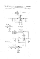
- FIG. 2 LOAD l6 FIGJA FIGJB I I FIGJC-FLIL- INPUT 3 FIG. 2 [2,;
- logic circuits are groups of electrical components interconnected to form standardized modules or building blocks which may be put together in any suitable combination to form a desired circuit.
- One type of logic circuit (called an AND gate) provides output signals only when a plurality of input signals coincide.
- Another type of logic circuit (called an OR gate) provides output signals when any one or more of a plurality of input signals are present.
- Still another logic circuit (called an INHIBIT gate) provides means for blocking signals under a specific condition.
- Yet another building block (called a FLIP-FLOP) provides a memory function.
- logic circuit modules or building blocks have no immediate use in and of themselves.
- these logic circuits are engineering aids which may be com- 'bined into an almost unlimited variety of circuits.
- logic circuits have featured electronic discharge devices such as tubes, transistors, and the like.
- tubes have excessive power requirements and transistors have temperature and other environmental limitations.
- an object of this invention is to provide new and improved logic circuits for use under widely varying temperatures.
- a magnetic amplifier having a core with a substantially square hysteresis loop characteristics is provided with reset and gate windings sequentially energized by the output of an AC generator, for example.
- the gate winding is energized to drive the core flux toward saturation of one magnetic polarity.
- the reset winding is energized to drive core flux away from saturation in that one polarity. Certain input signals nullify the effects of the reset winding. Thereafter, the magnetic core is saturated in the one polarity responsive to a succession of half-cycles of the first polarity.
- the gate winding Before the core is saturated, substantially all energy which the AC generator applies to the gate winding is utilized to drive the core flux toward magnetic saturation; therefore, the gate winding has a high DC impedance and little output current flows. After saturation, substantially no energy is dissi pated in driving the core flux, the gate winding offers very little DC impedance, and a large output current flows. A relatively large capacitance is connected to the gate Winding to give a smooth DC output potential, since the output current flows only during half-cycles of one polarity.
- a memory function is provided by feeding back a part of the filtered DC output to simulate an input signal, thus maintaining the output signal indefinitely. In this manner, the magnetic amplifier flips to remember the occurrence of an input signal. Later, a third or inhibit winding is energized causing the amplifier to flop and forget the original input signal while remembering the inhibit signal.
- FIG. 1 illustrates the concepts of a magnetic amplifier adapted to provide the basic elements of a logic circuit
- FIGS. 1A, 1B and 1C illustrate optional outputs of generator 4
- FIG. 2 illustrates a manner in which a plurality of electrically isolated input terminals may be provided to make gating circuits
- FIG. 3 shows a manner in which the magnetic amplifier may be modified to provide a more eflicient control or reset circuit
- FIG. 4 is a redrawing of FIG. 3 in the configuration of a balanced bridge circuit to facilitate an understanding of the improved efficiency of the circuit
- FIGS. 58 are examples illustrating the manner in which the basic concepts illustrated in FIGS. 1-4 may be combined to provide complete circuits.
- FIG. 5A illustrates how circuit components may be assembled to provide desired functions.
- FIG. 5B' is a logic diagram in which the functions of FIG. 5A are represented graphically by standard logic symbols.
- a Boolian algebra formula is also given to identify the logic functions, i.e. an output signal appears at terminal R if an input signal is applied at terminal A, and no signal is applied at terminals N1, N2, or N3.
- FIGS. 1-4 illustrate the basic concepts used to provide the logic circuits.
- the pedagogics of these figures is to explain the basic concepts in a step-by-step manner with each succeeding figure advancing an understanding of the technical principles involved.
- the basic circuit element is the magnetic core 10 having a substantially square hysteresis loop having a plurality of windings associated therewith. Dots near an end of each winding indicates the polarity thereof.
- Gate winding 2 is adapted to drive the flux of core 10 toward saturation of one magnetic polarity.
- Reset winding 1 and inhibit winding 13 are adapted to counteract the effects of winding 2 by driving the flux of core 10 away from saturation in the one magnetic polarity.
- An AC generator 4 provides alternating half-cycles which serve as a periodically reversing biasing potential.
- Half-cycles of one polarity (designated Eg) energize gate winding 2 and half-cycles of reverse polarity (designated Er) energize reset winding 1.
- the circuit values and the frequency of generator 4 are Such that a half-cycle of gating current Eg does not provide enough magnetic effects to switch core 10 from its first or unsaturated (with respect to the one magnetic polarity) state to its s cond or saturated state.
- the cumulative effects of gating current Eg are such that two half-cycles cause core 10 to switch from its unsaturated to its saturated condition unless reset current Er is applied during alternate half-cycles.
- Winding 1 is provided with a sufficient number of turns to cause core 10 to switch from its saturated to its unsaturated (with respect to the one magnetic polarity) condition in a single half-cycle of energizing current.
- Means are provided for reducing the size of the magnetic core by limiting the volt second product of the output of generator 4.
- generator 4 provides periodically changing control voltage polarities.
- a sine wave may be used as shown in FIG. 1A; however, the excessive volt seconds in each halfcycle require the use of a needlessly large core.
- the output signal of generator 4 is limited or reduced to a minimum by the use of pulses of a restricted duration as shown in FIG. 1B, thereby permitting the use of small cores.
- No specific durations or amplitudes are implied for the waveform 1B; although, in any specific .system, certain relationships regarding amplitude, duration and the properties of windings 1 and 2 exist for best performance.
- Detailed description Generator 4 develops a biasing voltage which is periodically applied across transformer 3 to the reset and gate windings 1 and 2.
- reset voltage Er may be of negative polarity, in which case the gating voltage Eg is of positive polarity.
- reset voltage Er is of positive polarity, and gating voltage Eg is of negative polarity.
- Diodes and 6 are poled oppositely so that current can not flow simultaneously in both winding 1 and winding 2.
- current flows through diode 5 and winding 1.
- gating voltage Eg is of positive polarity, and no current flows through either diode 6 or winding 2.
- core 10 is biased toward saturation by current which flows in winding 2. Then it is biased away from saturation by current which flows in winding 1.
- pacitor 9 stores and smooths this input signal, as required, to insure a coincidence of input and reset signals by, in effect, spreading the period of time during which the input signal appears.
- Resistance R provides a path for discharging capacitor 9 before the occurrence of a complete cycle in the output of generator 4.
- the input signal appearing at terminal 7 may be quite long or may be a momentary pulse. However, as long as the input signal remains at point 7, reset voltage Er is ineffective, winding 2 offers substantially no DC resistance, and current is delivered to load 16 during each halfcycle in the output of generator 4 which may be conducted through diode 6. Hence, the output of the magnetic amplifier is pulsating DC. Such a pulsating output may be desirable in some circuits. However, in these logic circuits, it is more desirable to provide a smooth DC output. Therefore, a relatively large capacitor 11 is connected to filter the output.
- One of the basic building blocks in logic systems is a memory device or FLIP-FLOP circuit.
- One input signal turns the circuit on, and a second input signal turns the circuit off.
- a FLIP-FLOP a small portion of the rectified half-cycle output signal fed through winding 2 to load 16 is bled-off at point 8 and fed-back through diode 12 to input 7.
- This feedback is a locking potential which back biases the diode 5 and prevents the reset voltage Er from energizing winding 1.
- core 10 remains in its saturated condition and output current continues to be delivered to load 16 without regard to the continuation of the original input signal at point 7.
- a suitable signal may be applied at point 15, thus energizing winding 13 to demagnetize core 10 with respect to the one magnetic polarity. Thereafter, if no input signal is applied at point 7, the circuit returns to its quiescent operation and substantially no current flows through winding 2 to load 16.
- FIG. 2 discloses how gate circuits may be made by providing a plurality of electrically isolated inputs.
- the amplifier of FIG. 2 is the same as the amplifier of FIG. 1 except that there is no inhibit winding and no memory feedback through diode 12. While an inhibit winding is necessary to turn off a flip flop it still may be employed in a logic circuit to force reset.
- the path for reset current extends from ground through the center tap of the upper winding of transformer 3 (where energy from generator 4 is introduced by a transformer action) winding 1, diode 5 and resistor R1 to ground.
- Resistor R1 is provided first to help reduce power consumption by eliminating the need for energizing a preceding circuit, second, to allow full use of all power in the input signal. It has been found that resistor R1 may be replaced by a diode or by a winding, as required.
- Diodes 21 and 23 are provided to isolate the OR gate input signals from each other. It is not possible for a direct current to flow from point 20 through diode 21 and diode 23 to point 22 because current which is passed by diode 21 is not passed by diode 23. On the other hand, input signals of the same polarity applied to either point 20 or 22 are passed through the diodes 21, 23 to point 7.
- FIG. 3 shows a magnetic amplifier having increased reset efiiciency
- FIG. 4 is a redrawing of a portion of FIG. 3
- Feedback resistor R2 is provided to introduce bias in a balanced bridge during the half-cycles when gating voltage Eg is efiective. That is, a balanced bridge circuit is provided wherein two arms of the bridge are the two halves of the secondary winding of transformer 3. One arm of the bridge is reset winding 1 and the other arm of the bridge is a control means in the form of resistor R2. When the bridge is in balance, a zero potential difference appears between points 41 and 42. Hence, all of the reset voltage Er is forced through winding 1. Resistor R1 is not required if the bridge is in perfect balance. However, since perfect balance is not possible, any potentials appearing at point 41 are connected to ground through resistor R1.
- FIG. 5A illustrates a circuit similar to that shown in FIG. 3, plus an inhibit winding 13.
- a signal source applies voltages Er and Eg of alternate polarity to reset and gate windings 1 and 2 respectively. If a signal is applied to any of the terminals N1, N2, or N3, inhibit winding 13 is energized to prevent core from saturating in the one magnetic direction despite any appearance of a signal at terminal A.
- the magnetic amplifier conducts if a signal is applied at terminal A and not at any of the three OR gate inputs.
- the circle marked INH indicates inhibit means such as winding 13 and the diameter line is slanted to indicate that it is the output of the amplifier which is blocked.
- FIG. 6A illustrates a FLIP-FLOP with a three input OR gate inhibitor.
- an output is delivered to terminal R when an input signal is applied at either of the terminals A or R and not at any of the inhibit terminals.
- the reset voltage Er is blocked and does not counteract the magnetic bias resulting from the preceding half-cycle.
- Winding 2 conducts to saturate core 10 and deliver an output current to terminal R. Thereafter, feedback through diode 12 maintains a blocking potential on the left side of diode 5. This prevents the reset winding from demagnetizing core 10 with respect to the given polarity.
- the circuit continues to deliver output current at terminal R until an inhibiting signal appears on any of the terminals N1-N3 at which time current flows in winding 13 to drive the core 10 away from saturation. Since diodes 12 and 21 are biased in the same effective direction relative to the reset winding 1, an input signal at terminal R has the same effect as a signal at terminal A.
- FIGS. 53 and 6B show an amplifier with a three input OR gate inhibitor. If a similar device is required in connection with a FLIP-FLOP, it is only necessary to connect the feedback circuit including diode 12 to form an input OR gate.
- FIG. 7 is a combination of AND gates and OR gates as logically shown in FIG. 7B.
- a signal must be applied to both of the terminals B and C if current in reset winding 1 is to be blocked. This provides an AND gate.
- Terminal A is equivalent to terminal B and, therefore, provides an OR gate preceding the AND gate.
- Diodes 12 and 12' are poled in the same direction as input diodes 82 (relative to the reset winding 1) to provide the feedback which forms a FLIP-FLOP circuit.
- an application of a potential to terminal N inhibits the output of the magnetic amplifier.
- FIG. 8 illustrates a cascaded combination of an OR gate, an AND gate, an OR gate, and amplifier and inhibitor. If a blocking signal is applied to terminal C, a by-pass circuit for reset voltage Er may be traced through diode 5 and resistor R4 to ground. Similarly, a signal applied to terminal B does not prevent a flow of reset current through diode 5. Therefore, both terminals B and C must have input signals applied thereto if the amplifier is to supply an output signal. Hence, terminals B and C comprise an AND gate. Once output current begins to flow through winding 2 and terminal R, feedback through diode 12 maintains conductivity to provide a FLIP-FLOP circuit.
- the inhibit winding 3 has a demagnetizing effect (with respect to the one magnetic polarity) so that an application of a signal to terminal N turns the amplifier off.
- Terminal A provides an OR gate to permit a control which is alternative to that of the AND gate, i.e. a signal at terminal A is applied through diodes 92 and 93 to block reset current without regard to any signals which then may be applied to terminals B and C.
- An electrical device comprising a square loop magnetic core having a plurality of windings associated there with, means for sequentially and alternately energizing two of said windings, one of said two windings driving core flux toward saturation in one magnetic direction, the other of said two windings driving core flux away from saturation in said one magnetic direction, means responsive to an input signal for blocking the effect on core flux when said other Winding is energized, whereby said core flux is driven to saturation responsive to repeated energizations of said one winding, means responsive to saturation of said core for feeding back a signal to hold said core in saturation, and means comprising another of said windings for driving said core flux away from saturation.
- a magnetic device having substantially square hysteresis loop characteristics, at least two windings associated with said magnetic device, means for providing biasing potential of periodically reversing polarity, a plurality of unidirectional means for conducting current of only one polarity, means for connecting one end of the first of said windings to one of said unidirectional means, means for applying said biasing potential to the other end of said first winding, means for connecting one end of the second of said windings to another of said unidirectional means, means for applying said biasing potential to the other end of said second Winding, means for applying input signals to said one unidirectional means, filter means connecting to said other unidirectional means, and means coupling said filter means to apply a feedback signal to said one unidirectional means to provide a locking potential for giving a flip-flop action.
- a magnetic amplifier comprising at least two windings associated with a magnetic core, a pair of interconnected transformer windings, means for cyclically applying biasing potential through said transformer windings to said two windings, means for connecting one end of a first of said two windings to a free end of said interconnected transformer windings, control means for connecting the other end of said first Winding to the other free end of said interconnected transformer windings, means whereby said first winding, said interconnected windings, and said control means complete a balanced bridge, means for applying input signals to the first of said two windings to prevent the flow of current responsive to said biasing potential through said first winding.
- means comprising a magnetic core having two stable states of saturation, supply means for providing alternating voltage having first and second half-cycles, means responsive to said first halfcycles for providing magnetizing effects to bias said core toward a first of said states of saturation, means responsive to said second half-cycles for reducing said magnetizing effects produced during said first half-cycles thereby biasing said core toward a second of said states of saturation, control means for changing the magnetizing effects of said second half cycles, means rendered operative responsive to last said named means for filtering said first half-cycles to provide a substantially smooth DC. signal, and means responsive to said DC. signal for maintaining said changed magnetizing effects, and means for thereafter feeding back a signal to the first of said two windings for a continuous prevention of said current flow into said first winding.
- the magnetic amplifier of claim 8 and means comprising a plurality of terminals for inhibiting said amplifier, and means for rendering said inhibiting means effective responsive to signals applied to any of said terminals.
- control means comprises an OR gate having a plurality of input terminals, and means responsive to signals applied to at least one of said input terminal for feeding back at least a portion of said filtered half-cycles through another of said OR gate input terminals thereby maintaining conductivity.
- the magnetic amplifier of claim 12 wherein said feedback means comprises unidirectional current control means for isolating said control means from said feedback means.
Landscapes
- Physics & Mathematics (AREA)
- Engineering & Computer Science (AREA)
- Computer Hardware Design (AREA)
- Computing Systems (AREA)
- General Engineering & Computer Science (AREA)
- Mathematical Physics (AREA)
- Amplifiers (AREA)
Description
May 28, 1968 A. J. RADCLIFF'E, JR 3,385,975 MAGNETIC LOGIC CIRCUITS HAVING A MAGNETIC AMPLIFIER CONFIGURATION Original Filed May 14, 1959 3 Sheets-Sheet 1 FIG.
LOAD l6 FIGJA FIGJB I I FIGJC-FLIL- INPUT 3 FIG. 2 [2,;
\NPUT Hi IN V EN TOR.
A.J. RADCLIFFE JR.
AT T0 RNEY May 28, 1968 A, J. RADCL IFFE, JR 8 5 MAGNETIC LOGIC CIRCUITS HAVING A MAGNETIC AMPLIFIER CONFIGURATION Original Filed May 14, 1959 5 Shees$heet 2 R4 HG. 5A
May '28, 1968 A. J. RADCLIFFE, JR 3,335,975
MAGNETIC LOGIC CIRCUITS HAVING A MAGNETIC AMPLIFIER CONFIGURATION Original Filed May 14, 1959 3 Sheets-Sheet 5 I R5 HG 7A N-- W v 2 A a0 la W 1 OR mu 5 c OR AMP United States Patent MAGNETlC LOGIC CIRCUITS HAVING A MAGNETIC AMPLIFIER CONFIGURATION Arthur J. Radclifie, .lr., Plymouth, Mich., assignor to International Telephone and Telegraph Corporation, New York, N.Y., a corporation of Maryland Continuation of application Ser. No. 813,141, May 14, 1959, now Patent No. 3,121,173, dated Feb. 11, 1964. This application Oct. 10, 1963, Ser. No. 315,167
13 Claims. (Cl. 307-88) ABSTRACT OF THE DISCLOSURE This invention relates to logic circuits and more particularly to logic circuits using magnetic amplifiers. This is a continuation of my application entitled, Logic Circuits, Ser. No. 813,141, filed May 14, 1959, and assigned to the assignee of this invention, now Patent Number 3,121,173.
Briefly, logic circuits are groups of electrical components interconnected to form standardized modules or building blocks which may be put together in any suitable combination to form a desired circuit. One type of logic circuit (called an AND gate) provides output signals only when a plurality of input signals coincide. Another type of logic circuit (called an OR gate) provides output signals when any one or more of a plurality of input signals are present. Still another logic circuit (called an INHIBIT gate) provides means for blocking signals under a specific condition. Yet another building block (called a FLIP-FLOP) provides a memory function.
Usually logic circuit modules or building blocks have no immediate use in and of themselves. Primarily, these logic circuits are engineering aids which may be com- 'bined into an almost unlimited variety of circuits. In the past, logic circuits have featured electronic discharge devices such as tubes, transistors, and the like. However, each of these devices have certain drawbacks. For example, tubes have excessive power requirements and transistors have temperature and other environmental limitations.
Accordingly, an object of this invention is to provide new and improved logic circuits for use under widely varying temperatures.
In accordance with this invention, a magnetic amplifier having a core with a substantially square hysteresis loop characteristics is provided with reset and gate windings sequentially energized by the output of an AC generator, for example. During half-cycles of a first polarity in the output of the AC generator, the gate winding is energized to drive the core flux toward saturation of one magnetic polarity. During half-cycles of opposite polarity in the output of the AC generator, the reset winding is energized to drive core flux away from saturation in that one polarity. Certain input signals nullify the effects of the reset winding. Thereafter, the magnetic core is saturated in the one polarity responsive to a succession of half-cycles of the first polarity. Before the core is saturated, substantially all energy which the AC generator applies to the gate winding is utilized to drive the core flux toward magnetic saturation; therefore, the gate winding has a high DC impedance and little output current flows. After saturation, substantially no energy is dissi pated in driving the core flux, the gate winding offers very little DC impedance, and a large output current flows. A relatively large capacitance is connected to the gate Winding to give a smooth DC output potential, since the output current flows only during half-cycles of one polarity.
A memory function is provided by feeding back a part of the filtered DC output to simulate an input signal, thus maintaining the output signal indefinitely. In this manner, the magnetic amplifier flips to remember the occurrence of an input signal. Later, a third or inhibit winding is energized causing the amplifier to flop and forget the original input signal while remembering the inhibit signal.
The above mentioned and other objects of this invention together with the manner of obtaining them will be come more apparent and the invention itself will be best understood by making reference to the following description of an embodiment of the invention taken in conjunction with the accompanying drawings in which:
FIG. 1 illustrates the concepts of a magnetic amplifier adapted to provide the basic elements of a logic circuit;
FIGS. 1A, 1B and 1C illustrate optional outputs of generator 4;
FIG. 2 illustrates a manner in which a plurality of electrically isolated input terminals may be provided to make gating circuits;
FIG. 3 shows a manner in which the magnetic amplifier may be modified to provide a more eflicient control or reset circuit;
FIG. 4 is a redrawing of FIG. 3 in the configuration of a balanced bridge circuit to facilitate an understanding of the improved efficiency of the circuit; and
FIGS. 58 are examples illustrating the manner in which the basic concepts illustrated in FIGS. 1-4 may be combined to provide complete circuits.
Each of the circuits shown in FIGS. 5-8 includes three parts. For example, FIG. 5A illustrates how circuit components may be assembled to provide desired functions. FIG. 5B'is a logic diagram in which the functions of FIG. 5A are represented graphically by standard logic symbols. A Boolian algebra formula is also given to identify the logic functions, i.e. an output signal appears at terminal R if an input signal is applied at terminal A, and no signal is applied at terminals N1, N2, or N3.
Brief description FIGS. 1-4 illustrate the basic concepts used to provide the logic circuits. The pedagogics of these figures is to explain the basic concepts in a step-by-step manner with each succeeding figure advancing an understanding of the technical principles involved.
Briefly, the basic circuit element is the magnetic core 10 having a substantially square hysteresis loop having a plurality of windings associated therewith. Dots near an end of each winding indicates the polarity thereof. Gate winding 2 is adapted to drive the flux of core 10 toward saturation of one magnetic polarity. Reset winding 1 and inhibit winding 13 are adapted to counteract the effects of winding 2 by driving the flux of core 10 away from saturation in the one magnetic polarity.
An AC generator 4 provides alternating half-cycles which serve as a periodically reversing biasing potential. Half-cycles of one polarity (designated Eg) energize gate winding 2 and half-cycles of reverse polarity (designated Er) energize reset winding 1. The circuit values and the frequency of generator 4 are Such that a half-cycle of gating current Eg does not provide enough magnetic effects to switch core 10 from its first or unsaturated (with respect to the one magnetic polarity) state to its s cond or saturated state. However, the cumulative effects of gating current Eg are such that two half-cycles cause core 10 to switch from its unsaturated to its saturated condition unless reset current Er is applied during alternate half-cycles. Winding 1 is provided with a sufficient number of turns to cause core 10 to switch from its saturated to its unsaturated (with respect to the one magnetic polarity) condition in a single half-cycle of energizing current.
Means are provided for reducing the size of the magnetic core by limiting the volt second product of the output of generator 4. The important thing about generator 4 is that it provides periodically changing control voltage polarities. A sine wave may be used as shown in FIG. 1A; however, the excessive volt seconds in each halfcycle require the use of a needlessly large core. The same results may be had if the output signal of generator 4 is limited or reduced to a minimum by the use of pulses of a restricted duration as shown in FIG. 1B, thereby permitting the use of small cores. No specific durations or amplitudes are implied for the waveform 1B; although, in any specific .system, certain relationships regarding amplitude, duration and the properties of windings 1 and 2 exist for best performance.
At an instant, it may be assumed that core is in its non-saturated state with respect to one magnetic polarity. Reset voltage Er is assumed to be positive; therefore, no current flows through winding 1 and diode 5. Gate voltage Eg is negative and current does flow through winding 2 and diode 6. Responsive to the current through the winding 2, the flux in core 10 is driven toward saturation in the one magnetic polarity. However, in the single halfcycle being described, core 10 can not reach its second or saturated state. Also during the half-cycle being de scribed, winding 2 offers relatively great DC resistance to current flow. Thus substantially all of the energy that is introduced through transformer 3 is absorbed across winding 2 and none across load 16. When the half-cycle being described terminates, core 10 remains in the state of partial magnetic saturation to which it has been driven.
When the control current from generator 4 reaches the next half-cycle, reset voltage Er is negative and gate voltage Eg is positive. Current flows through diode 5 and winding 1 While diode 6 blocks current flow in Winding 2. Since opposite magnetic effects are produced by windings 1 and 2, the flux in core 10 is driven away from the partial saturation in the one magnetic polarity. Therefore, core 10 is now biased toward its unsaturated condition with respect to the one magnetic polarity.
The following and every succeeding cycle repeats the process. First, core 10 is biased toward saturation by current which flows in winding 2. Then it is biased away from saturation by current which flows in winding 1.
Next, assume that an input voltage is applied at point 7 with a potential which is more negative than the potential of reset voltage Er, thus back biasing diode 5. Ca-
pacitor 9 stores and smooths this input signal, as required, to insure a coincidence of input and reset signals by, in effect, spreading the period of time during which the input signal appears. Resistance R provides a path for discharging capacitor 9 before the occurrence of a complete cycle in the output of generator 4.
Under these assumed conditions, no current flows in winding 1 due to the blocking effect of the back biased diode 5. The magnetic effects caused by energization of gate winding 2, are not overcome on the next half-cycle. Therefore, core 16 remains biased toward, but not in a condition of saturation in the one magnetic polarity. When current flows through gate winding 2 on the next half-cycle after the reset voltage is blocked by an input signal, the flux of core 10 is again driven toward saturation in the one magnetic polarity. The magnetic effects are cumulative, and after the volt-second content of a sufficient number of half-cycles are integrated, the flux of core 10 is driven to full saturation in the one magnetic polarity. Then, the effective DC resistance of winding 2 falls from a relatively high value to an extremely low value, and energy from generator 4 reaches the load 16.
The input signal appearing at terminal 7 may be quite long or may be a momentary pulse. However, as long as the input signal remains at point 7, reset voltage Er is ineffective, winding 2 offers substantially no DC resistance, and current is delivered to load 16 during each halfcycle in the output of generator 4 which may be conducted through diode 6. Hence, the output of the magnetic amplifier is pulsating DC. Such a pulsating output may be desirable in some circuits. However, in these logic circuits, it is more desirable to provide a smooth DC output. Therefore, a relatively large capacitor 11 is connected to filter the output.
One of the basic building blocks in logic systems is a memory device or FLIP-FLOP circuit. One input signal turns the circuit on, and a second input signal turns the circuit off. To provide a FLIP-FLOP" circuit, a small portion of the rectified half-cycle output signal fed through winding 2 to load 16 is bled-off at point 8 and fed-back through diode 12 to input 7. This feedback is a locking potential which back biases the diode 5 and prevents the reset voltage Er from energizing winding 1. Thus, core 10 remains in its saturated condition and output current continues to be delivered to load 16 without regard to the continuation of the original input signal at point 7. To return the FLIP-FLOP to its original state, a suitable signal may be applied at point 15, thus energizing winding 13 to demagnetize core 10 with respect to the one magnetic polarity. Thereafter, if no input signal is applied at point 7, the circuit returns to its quiescent operation and substantially no current flows through winding 2 to load 16.
FIG. 2 discloses how gate circuits may be made by providing a plurality of electrically isolated inputs. Briefly, the amplifier of FIG. 2 is the same as the amplifier of FIG. 1 except that there is no inhibit winding and no memory feedback through diode 12. While an inhibit winding is necessary to turn off a flip flop it still may be employed in a logic circuit to force reset. Here the path for reset current extends from ground through the center tap of the upper winding of transformer 3 (where energy from generator 4 is introduced by a transformer action) winding 1, diode 5 and resistor R1 to ground. Resistor R1 is provided first to help reduce power consumption by eliminating the need for energizing a preceding circuit, second, to allow full use of all power in the input signal. It has been found that resistor R1 may be replaced by a diode or by a winding, as required.
If a signal is applied at either point 20 or point 22, the diode 5 is back biased, and reset current is effectively blocked. Removal of an input signal from point 26, without removal of an input signal from point 22 (and vice versa) does not have any effect. It is only when input signals are simultaneously removed from both of the input terminals 20 and 22 that the magnetic amplifier of FIG. 2 is turned off. Therefore, the embodiment of FIG. 2 provides an OR gate.
FIG. 3 shows a magnetic amplifier having increased reset efiiciency (FIG. 4 is a redrawing of a portion of FIG. 3). Feedback resistor R2 is provided to introduce bias in a balanced bridge during the half-cycles when gating voltage Eg is efiective. That is, a balanced bridge circuit is provided wherein two arms of the bridge are the two halves of the secondary winding of transformer 3. One arm of the bridge is reset winding 1 and the other arm of the bridge is a control means in the form of resistor R2. When the bridge is in balance, a zero potential difference appears between points 41 and 42. Hence, all of the reset voltage Er is forced through winding 1. Resistor R1 is not required if the bridge is in perfect balance. However, since perfect balance is not possible, any potentials appearing at point 41 are connected to ground through resistor R1.
The following is a description of a few typical applications illustrating how the principles described above may be used to provide a wide variety of more sophisticated circuits. Those skilled in the art will readily perceive any number of other combinations for meeting other needs. The same reference numerals identify corresponding parts in all figures.
FIG. 5A illustrates a circuit similar to that shown in FIG. 3, plus an inhibit winding 13. During quiescent periods, a signal source applies voltages Er and Eg of alternate polarity to reset and gate windings 1 and 2 respectively. If a signal is applied to any of the terminals N1, N2, or N3, inhibit winding 13 is energized to prevent core from saturating in the one magnetic direction despite any appearance of a signal at terminal A. As indicated by FIG. 5B, the magnetic amplifier conducts if a signal is applied at terminal A and not at any of the three OR gate inputs. The circle marked INH indicates inhibit means such as winding 13 and the diameter line is slanted to indicate that it is the output of the amplifier which is blocked.
FIG. 6A illustrates a FLIP-FLOP with a three input OR gate inhibitor. Here an output is delivered to terminal R when an input signal is applied at either of the terminals A or R and not at any of the inhibit terminals. When a signal is applied at input terminal A, the reset voltage Er is blocked and does not counteract the magnetic bias resulting from the preceding half-cycle. On the next half cycle, Winding 2 conducts to saturate core 10 and deliver an output current to terminal R. Thereafter, feedback through diode 12 maintains a blocking potential on the left side of diode 5. This prevents the reset winding from demagnetizing core 10 with respect to the given polarity. Thus, the circuit continues to deliver output current at terminal R until an inhibiting signal appears on any of the terminals N1-N3 at which time current flows in winding 13 to drive the core 10 away from saturation. Since diodes 12 and 21 are biased in the same effective direction relative to the reset winding 1, an input signal at terminal R has the same effect as a signal at terminal A.
A comparison of the logic diagrams of FIGS. 53 and 6B illustrates how the same basic circuit may be modified by an additional element to provide additional features. For example, both FIGS. 5B and 6B show an amplifier with a three input OR gate inhibitor. If a similar device is required in connection with a FLIP-FLOP, it is only necessary to connect the feedback circuit including diode 12 to form an input OR gate.
FIG. 7 is a combination of AND gates and OR gates as logically shown in FIG. 7B. Here a signal must be applied to both of the terminals B and C if current in reset winding 1 is to be blocked. This provides an AND gate. Terminal A is equivalent to terminal B and, therefore, provides an OR gate preceding the AND gate. Diodes 12 and 12' are poled in the same direction as input diodes 82 (relative to the reset winding 1) to provide the feedback which forms a FLIP-FLOP circuit. As in previously described circuits, an application of a potential to terminal N inhibits the output of the magnetic amplifier.
FIG. 8 illustrates a cascaded combination of an OR gate, an AND gate, an OR gate, and amplifier and inhibitor. If a blocking signal is applied to terminal C, a by-pass circuit for reset voltage Er may be traced through diode 5 and resistor R4 to ground. Similarly, a signal applied to terminal B does not prevent a flow of reset current through diode 5. Therefore, both terminals B and C must have input signals applied thereto if the amplifier is to supply an output signal. Hence, terminals B and C comprise an AND gate. Once output current begins to flow through winding 2 and terminal R, feedback through diode 12 maintains conductivity to provide a FLIP-FLOP circuit. The inhibit winding 3 has a demagnetizing effect (with respect to the one magnetic polarity) so that an application of a signal to terminal N turns the amplifier off. Terminal A provides an OR gate to permit a control which is alternative to that of the AND gate, i.e. a signal at terminal A is applied through diodes 92 and 93 to block reset current without regard to any signals which then may be applied to terminals B and C.
While the principles of the invention have been described in connection With the specific apparatus, it is to be clearly understood that this description is made only by way of example and not as a limitation on the scope of the invention.
I claim:
1. An electrical device comprising a square loop magnetic core having a plurality of windings associated there with, means for sequentially and alternately energizing two of said windings, one of said two windings driving core flux toward saturation in one magnetic direction, the other of said two windings driving core flux away from saturation in said one magnetic direction, means responsive to an input signal for blocking the effect on core flux when said other Winding is energized, whereby said core flux is driven to saturation responsive to repeated energizations of said one winding, means responsive to saturation of said core for feeding back a signal to hold said core in saturation, and means comprising another of said windings for driving said core flux away from saturation.
2. In an electrical logic circuit, a magnetic device having substantially square hysteresis loop characteristics, at least two windings associated with said magnetic device, means for providing biasing potential of periodically reversing polarity, a plurality of unidirectional means for conducting current of only one polarity, means for connecting one end of the first of said windings to one of said unidirectional means, means for applying said biasing potential to the other end of said first winding, means for connecting one end of the second of said windings to another of said unidirectional means, means for applying said biasing potential to the other end of said second Winding, means for applying input signals to said one unidirectional means, filter means connecting to said other unidirectional means, and means coupling said filter means to apply a feedback signal to said one unidirectional means to provide a locking potential for giving a flip-flop action.
3. The electrical logic circuit of claim 2 wherein said one unidirectional means is poled to conduct one polarity of said biasing potential and said other unidirectional means is poled to conduct the other polarity of said biasing potential.
4. The electrical logic circuit of claim 2 and means for interconnecting components of said logic circuits in a balanced bridge configuration whereby said first winding comprises a first arm of said bridge, said means for providing biasing potential comprises second and third arms of said bridge, and control means connected in a fourth arm of said bridge to provide a balanced bridge.
5. The electrical logic circuit of claim 2 and a plurality of input terminals, means for electrically isolating said input terminals thereby providing an OR gate for coupling a plurality of sources of input signals to said one unidirectional means.
6. The electrical logic circuit of claim 5 and means connected between said one unidirectional means and said isolated input means for conducting said biasing potential thereby providing a path for energizing said first winding.
7. A magnetic amplifier comprising at least two windings associated with a magnetic core, a pair of interconnected transformer windings, means for cyclically applying biasing potential through said transformer windings to said two windings, means for connecting one end of a first of said two windings to a free end of said interconnected transformer windings, control means for connecting the other end of said first Winding to the other free end of said interconnected transformer windings, means whereby said first winding, said interconnected windings, and said control means complete a balanced bridge, means for applying input signals to the first of said two windings to prevent the flow of current responsive to said biasing potential through said first winding.
8. In a magnetic amplifier, means comprising a magnetic core having two stable states of saturation, supply means for providing alternating voltage having first and second half-cycles, means responsive to said first halfcycles for providing magnetizing effects to bias said core toward a first of said states of saturation, means responsive to said second half-cycles for reducing said magnetizing effects produced during said first half-cycles thereby biasing said core toward a second of said states of saturation, control means for changing the magnetizing effects of said second half cycles, means rendered operative responsive to last said named means for filtering said first half-cycles to provide a substantially smooth DC. signal, and means responsive to said DC. signal for maintaining said changed magnetizing effects, and means for thereafter feeding back a signal to the first of said two windings for a continuous prevention of said current flow into said first winding.
9. The magnetic amplifier of claim 8 and means comprising a plurality of terminals for inhibiting said amplifier, and means for rendering said inhibiting means effective responsive to signals applied to any of said terminals.
14 The magnetic amplifier of claim 8 wherein said means responsive to said second half-cycles is connected as a first arm of a balanced bridge, said means for providing said alternating voltage is connected as second and third arms of said balanced bridge and means comprising a resistor connected as the fourth arm of said balanced bridge.
11. The magnetic amplifier of claim 8 wherein said control means comprises an OR gate having a plurality of input terminals, and means responsive to signals applied to at least one of said input terminal for feeding back at least a portion of said filtered half-cycles through another of said OR gate input terminals thereby maintaining conductivity.
12. The magnetic amplifier of claim 8 and feedback means for applying to said control means a signal derived from said filtered first half-cycles.
13. The magnetic amplifier of claim 12 wherein said feedback means comprises unidirectional current control means for isolating said control means from said feedback means.
References Cited UNITED STATES PATENTS 2,871,442 11/1959 Perkins 30788 X BERNARD KONICK, Primary Examiner.
S. URYNOWICZ, Assistant Examiner.
Priority Applications (1)
| Application Number | Priority Date | Filing Date | Title |
|---|---|---|---|
| US315167A US3385975A (en) | 1963-10-10 | 1963-10-10 | Magnetic logic circuits having a magnetic amplifier configuration |
Applications Claiming Priority (1)
| Application Number | Priority Date | Filing Date | Title |
|---|---|---|---|
| US315167A US3385975A (en) | 1963-10-10 | 1963-10-10 | Magnetic logic circuits having a magnetic amplifier configuration |
Publications (1)
| Publication Number | Publication Date |
|---|---|
| US3385975A true US3385975A (en) | 1968-05-28 |
Family
ID=23223197
Family Applications (1)
| Application Number | Title | Priority Date | Filing Date |
|---|---|---|---|
| US315167A Expired - Lifetime US3385975A (en) | 1963-10-10 | 1963-10-10 | Magnetic logic circuits having a magnetic amplifier configuration |
Country Status (1)
| Country | Link |
|---|---|
| US (1) | US3385975A (en) |
Citations (1)
| Publication number | Priority date | Publication date | Assignee | Title |
|---|---|---|---|---|
| US2871442A (en) * | 1957-11-14 | 1959-01-27 | Westinghouse Electric Corp | Magnetic amplifier system |
-
1963
- 1963-10-10 US US315167A patent/US3385975A/en not_active Expired - Lifetime
Patent Citations (1)
| Publication number | Priority date | Publication date | Assignee | Title |
|---|---|---|---|---|
| US2871442A (en) * | 1957-11-14 | 1959-01-27 | Westinghouse Electric Corp | Magnetic amplifier system |
Similar Documents
| Publication | Publication Date | Title |
|---|---|---|
| US2809303A (en) | Control systems for switching transistors | |
| US2994788A (en) | Transistorized core flip-flop | |
| US2710928A (en) | Magnetic control for scale of two devices | |
| US3204172A (en) | Semiconductor controlled rectifier circuits | |
| US2920213A (en) | Transistor-magnetic core bi-stable circuit | |
| US2717965A (en) | High speed magnetic trigger circuit | |
| US3385975A (en) | Magnetic logic circuits having a magnetic amplifier configuration | |
| US2792506A (en) | Resettable delay flop | |
| US3121173A (en) | Logic circuits | |
| US3287574A (en) | Regenerative and-gate circuit producing output during shaping-pulse input upon coincidence with but regardless of continuous presence of other input | |
| US2947883A (en) | Square wave generator and diode modulator | |
| US2854586A (en) | Magnetic amplifier circuit | |
| US2766420A (en) | Magnetic coincidence detector | |
| US3074031A (en) | Magnetically controlled switching circuit | |
| US3229267A (en) | Magnetic core device | |
| US3238445A (en) | Saturable core pulse width control apparatus | |
| US2913594A (en) | Quarter adder | |
| US3032663A (en) | Pulse generator | |
| US3108258A (en) | Electronic circuit | |
| US3202807A (en) | Multiplication by varying amplitude and period of output pulse | |
| US2762935A (en) | Magnetic device | |
| US3275949A (en) | Saturable core pulse width modulator | |
| US3003067A (en) | Pulse counters | |
| US2798168A (en) | Magnetic amplifier and flip-flop circuit embodying the same | |
| US3085164A (en) | Amplifier having constant sinusoidal output voltage which is relatively independent of input shape |
Legal Events
| Date | Code | Title | Description |
|---|---|---|---|
| AS | Assignment |
Owner name: ITT CORPORATION Free format text: CHANGE OF NAME;ASSIGNOR:INTERNATIONAL TELEPHONE AND TELEGRAPH CORPORATION;REEL/FRAME:004389/0606 Effective date: 19831122 |