US3290583A - Voltage regulators - Google Patents
Voltage regulators Download PDFInfo
- Publication number
- US3290583A US3290583A US253730A US25373063A US3290583A US 3290583 A US3290583 A US 3290583A US 253730 A US253730 A US 253730A US 25373063 A US25373063 A US 25373063A US 3290583 A US3290583 A US 3290583A
- Authority
- US
- United States
- Prior art keywords
- transistor
- output
- oscillator
- terminals
- base
- Prior art date
- Legal status (The legal status is an assumption and is not a legal conclusion. Google has not performed a legal analysis and makes no representation as to the accuracy of the status listed.)
- Expired - Lifetime
Links
- 230000001419 dependent effect Effects 0.000 claims description 4
- 238000004804 winding Methods 0.000 description 29
- 239000003990 capacitor Substances 0.000 description 19
- 230000001276 controlling effect Effects 0.000 description 3
- 230000001105 regulatory effect Effects 0.000 description 2
- YXIWHUQXZSMYRE-UHFFFAOYSA-N 1,3-benzothiazole-2-thiol Chemical compound C1=CC=C2SC(S)=NC2=C1 YXIWHUQXZSMYRE-UHFFFAOYSA-N 0.000 description 1
- 238000010586 diagram Methods 0.000 description 1
- 238000007599 discharging Methods 0.000 description 1
- 230000001939 inductive effect Effects 0.000 description 1
Images
Classifications
-
- H—ELECTRICITY
- H02—GENERATION; CONVERSION OR DISTRIBUTION OF ELECTRIC POWER
- H02M—APPARATUS FOR CONVERSION BETWEEN AC AND AC, BETWEEN AC AND DC, OR BETWEEN DC AND DC, AND FOR USE WITH MAINS OR SIMILAR POWER SUPPLY SYSTEMS; CONVERSION OF DC OR AC INPUT POWER INTO SURGE OUTPUT POWER; CONTROL OR REGULATION THEREOF
- H02M3/00—Conversion of DC power input into DC power output
- H02M3/02—Conversion of DC power input into DC power output without intermediate conversion into AC
- H02M3/04—Conversion of DC power input into DC power output without intermediate conversion into AC by static converters
Definitions
- a voltage regulator comprises in combination a pair of input terminals for connection to the supply to be regulated, a pair of output terminals for connection to a load, a transistor having its emitter and collector connected between one of the input terminals and one of the output terminals, a square wave oscillator operable by said supply to produce an output consisting of successive positive and negative half-cycles, a pair of switching circuits through which the output from the oscillator is applied to the base of the transistor so that at the commencement of each half-cycle of the oscillator the transistor is rendered conductive, and means for interrupting the supply to the base of the transistor at a time in each half-cycle which is variable in accordance with the supply voltage across the output terminals.
- a pair of input terminals 1, 2 which are connected to a DC. source 3, and a pair of output terminals 4, 5 between which a load 6 is connected.
- the terminals 2, 5 are interconnected, whilst the terminal 1 is connected to the emitter of a transistor 7 having its collector connected to the terminal 4.
- the base of the transistor 7 is connected to one end of the secondary winding 8 of a transformer 9 through a diode 10 in series with a resistor 11, and is further connected to the other end of the winding 8 through a diode 12 in series with a resistor 13.
- the centre point of the winding 8 is connected to the terminal 1.
- Opposite ends of the winding 8 are connected to the anodes of controlled 'rectifiers 14, 15 respectively, the cathodes of these controlled rectifiers being interconnected, and the gates of the controlled rectifiers being connected to their respective cathodes through diodes 16, 17.
- the cathodes of the controlled rectifiers 14, 15 are connected through a resistor 80 to the base of the transistor 7.
- the transformer 9 further includes a primary winding 18 and control windings 19, 20.
- the windings 19, 26 each have one end connected through resistors 23, 24 respectively to the bases of transistors 21, 22. Moreover, the other end of the windings 19, are connected through a diode 25 to the emitter of the transistors 21, 22.
- the collectors of the transistors 21, 22 are connected to opposite ends of the winding 18, whilst said other end of the winding 19 is connected to the mid-point of the winding 18 through resistors 26, 27 in series. The point intermediate the resistors 26, 27 is connected to the terminal 2.
- the terminals 4, 5 are bridged by two parallel circuits, one of which contains a diode 28, and the other of which contains a resistor 29 in series with a resistor 30, the resistor 30 being bridged by a capacitor 31.
- a variable point on the resistor 31 is connected through a resistor 32 to the base of a transistor 33, the emitter of which is connected to the terminal 2 through a Zener diode 34 bridged by a capacitor 35.
- the base and collector of the transistor 33 are bridged by a capacitor 36 and a resistor 37 in series, whilst the emitter of the transistor 33 is connected through a resistor 38 to the terminal 1.
- the unijunction transistor 46 has its primary and secondary base terminals bridged by a Zener diode 47 having a capacitor 48 in parallel therewith. Moreover, the secondary base terminal of the unijunction transistor is connected to the terminal 2 through a resistor 49 which is bridged by the primary winding 50 of a transformer 51 having secondary windings 52, 53. One end of the winding 52 is connected through a resistor 54 to the gate of the controlled rectifier 15 whilst its other end is connected to the cathode of the controlled rectifier. One end of the winding 53 is connected through a resistor 55 to the gate of the controlled rectifier 14, whilst its other end is connected to the cathode of the controlled rectifier 14.
- the capacitor 45 is bridged by the collector and emitter of a transistor 56, the base of which is connected through a diode 57 to the terminal 2, and through a capacitor 58 and resistor 59 in series to the mid-point of the winding 18.
- the transformer 9 together with the components associated with its windings 18, 19, 20 form a square wave oscillator of known form.
- the output of the oscillator can be considered to consist of odd and even half-cycles.
- the emitter of the transistor 7 is of course connected to the midpoint of winding 8 during both the odd and even half-cycles, and during the odd half-cycles the base of the transistor 7 is connected to said other end of the winding 8 through a switching circuit constituted by the diode 12 and resistor 13. During the even half cycles, the base of the transistor 7 is connected to said one end of the Winding 8 through a further switching circuit constituted by the diode 10' and the resistor 11. In either case, therefore, the transistor is rendered conductive to permit current flow to the load.
- the controlled rectifier 15 is rendered conductive whilst the controlled rectifier 14 is unaffected.
- the transistor 7 is not only short circuited but actually has its base-emitter junction reversebiased by the conducting controlled rectifier and so the transistor 7 is turned off and no current flows to the output terminal 4.
- the oscillator and controlled rectifiers may be used to control more than one transistor. For each additional transistor five extra components are required, these components being those corresponding to resistors 18, 11 and 13, and diodes and 12.
- a DC. voltage regulator comprising in combination a pair of input terminals for connection to the supply to be regulated, a pair of output terminals for connection to a load, a transistor having its emitter and collector connected between one of the input terminals and one of the output terminals, a square wave oscillator connected across said input terminals so as to be operable by said supply, said square wave oscillator producing an output consisting of successive positive and negative half-cycles, a pair of switching circuits through which the output from the oscillator is applied to the base of the transistor so that at the commencement of each half-cycle of the oscillator the transistor is rendered conductive, switch means in circuit with the base-emitter junction of said transistor, said switch means when conductive reverse biasing said base-emitter junction to turn said transistor oil, and control means for said switch means, said control means being connected across said output terminals and controlling said switch means to turn ofl said transistor at a 'time in each half-cycle which is variable in accordance with the supply voltage across the output terminals.
- a DC. voltage regulator comprising in combination a pair of input terminals, a pair of output terminals, a D-.C. source connected between the input terminals, a load connected between the output terminals, a transistor having its collector and emitter connected between one of the input terminals and one of the output terminals, the other input terminal being connected to the other output terminal, a square wave oscillator connected across said input terminals so as to be operable by said D.C.
- a DC voltage regulator as claimed in claim 3 including a control transistor for controlling the charging rate of said capacitor, means for maintaining the emitter voltage 'of said control transistor constant, and means for applying a proportion of the voltage across said output terminals to the base of said control transistor.
- a DC voltage regulator as claimed in claim 4 including a series transductor connected in series with said transistor connected between the input and output terminals, and a [full wave rectifier through which the transductor output is connected to the base of said control transistor, where-by the charging rate of the capacitor is increased when the current flowing to the output terminal exceeds a predetermined value.
Landscapes
- Engineering & Computer Science (AREA)
- Power Engineering (AREA)
- Dc-Dc Converters (AREA)
Description
'Dec. 6, 1966 w. SINCLAIR 3,290,583
VOLTAGE REGULATORS Filed Jan. 24, 1963 United States Patent 3,290,583 VOLTAGE REGULATORS Walter Sinclair, Hemel Hempstead, England, assignor to Rotax Limited, London, England Filed Jan. 24, 1963, Ser. No. 253,730 Claims priority, application Great Britain, Feb. 6, 1962, 4,463/ 62 6 Claims. (Cl. 3239) This invention relates to voltage regulators of the kind in which a DC. supply circuit is broken intermittently for periods sufiicient to maintain the average voltage at a desired value.
A voltage regulator according to the invention comprises in combination a pair of input terminals for connection to the supply to be regulated, a pair of output terminals for connection to a load, a transistor having its emitter and collector connected between one of the input terminals and one of the output terminals, a square wave oscillator operable by said supply to produce an output consisting of successive positive and negative half-cycles, a pair of switching circuits through which the output from the oscillator is applied to the base of the transistor so that at the commencement of each half-cycle of the oscillator the transistor is rendered conductive, and means for interrupting the supply to the base of the transistor at a time in each half-cycle which is variable in accordance with the supply voltage across the output terminals.
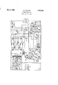
The accompanying drawing is a circuit diagram illustrating one example of the invention.
Referring to the drawing, there are provided a pair of input terminals 1, 2 which are connected to a DC. source 3, and a pair of output terminals 4, 5 between which a load 6 is connected. The terminals 2, 5 are interconnected, whilst the terminal 1 is connected to the emitter of a transistor 7 having its collector connected to the terminal 4.
The base of the transistor 7 is connected to one end of the secondary winding 8 of a transformer 9 through a diode 10 in series with a resistor 11, and is further connected to the other end of the winding 8 through a diode 12 in series with a resistor 13. The centre point of the winding 8 is connected to the terminal 1. Opposite ends of the winding 8 are connected to the anodes of controlled ' rectifiers 14, 15 respectively, the cathodes of these controlled rectifiers being interconnected, and the gates of the controlled rectifiers being connected to their respective cathodes through diodes 16, 17. Moreover, the cathodes of the controlled rectifiers 14, 15 are connected through a resistor 80 to the base of the transistor 7.
The transformer 9 further includes a primary winding 18 and control windings 19, 20. The windings 19, 26 each have one end connected through resistors 23, 24 respectively to the bases of transistors 21, 22. Moreover, the other end of the windings 19, are connected through a diode 25 to the emitter of the transistors 21, 22. The collectors of the transistors 21, 22 are connected to opposite ends of the winding 18, whilst said other end of the winding 19 is connected to the mid-point of the winding 18 through resistors 26, 27 in series. The point intermediate the resistors 26, 27 is connected to the terminal 2.
The terminals 4, 5 are bridged by two parallel circuits, one of which contains a diode 28, and the other of which contains a resistor 29 in series with a resistor 30, the resistor 30 being bridged by a capacitor 31. A variable point on the resistor 31 is connected through a resistor 32 to the base of a transistor 33, the emitter of which is connected to the terminal 2 through a Zener diode 34 bridged by a capacitor 35. The base and collector of the transistor 33 are bridged by a capacitor 36 and a resistor 37 in series, whilst the emitter of the transistor 33 is connected through a resistor 38 to the terminal 1.
3,290,583 Patented Dec. 6, 1966 The collector of the transistor 33 is further connected through a resistor 39 to the base of a transistor 40, the collector and emitter of which are bridged by a variable resistor 42 the emitter of which is connected to the terminal 1 through a resistor 41, and the base of which is connected to the terminal 1 through a resistor 43 in series with the resistor 41. The collector of the transistor 40 is connected to the terminal 2 through a resistor 44 in series with a capacitor 45, a point intermediate the resistor 44 and capacitor 45 being connected to the emitter of a unijunction transistor 46.
The unijunction transistor 46 has its primary and secondary base terminals bridged by a Zener diode 47 having a capacitor 48 in parallel therewith. Moreover, the secondary base terminal of the unijunction transistor is connected to the terminal 2 through a resistor 49 which is bridged by the primary winding 50 of a transformer 51 having secondary windings 52, 53. One end of the winding 52 is connected through a resistor 54 to the gate of the controlled rectifier 15 whilst its other end is connected to the cathode of the controlled rectifier. One end of the winding 53 is connected through a resistor 55 to the gate of the controlled rectifier 14, whilst its other end is connected to the cathode of the controlled rectifier 14.
The capacitor 45 is bridged by the collector and emitter of a transistor 56, the base of which is connected through a diode 57 to the terminal 2, and through a capacitor 58 and resistor 59 in series to the mid-point of the winding 18.
Between the collector of the transistor 7 and the terminal 4 is a series transductor which is connected to a full-wave bridge rectifier 61, and derives its AC. power from a transformer 63 having a primary winding 64 and secondary winding 62.
Connected across the output of the full-wave bridge rectifier are three parallel circuits containing respectively a resistor 65, a resistor 66, and a diode 67 and capacitor 68 in series. A point intermediate the diode 67 and capacitor 68 is connected through a diode 69 to the base of the transistor 33, and through a diode 7 0* to the emitter of the transistor 33. The transformer 9 together with the components associated with its windings 18, 19, 20 form a square wave oscillator of known form. On switching on current flows through the resistor 26 and Winding 19 to switch on the transistor 21 and the resulting flow through the winding 18 induces a feed-back signal to the base of the transistor 21 to render it more conductive, whilst at the same time inducing a signal in the winding 20 to hold the transistor 22 off. However, when the transistor 21 is fully conductive, there is no further feedback and the transistor 22 becomes conductive, the transistor 21 being switched oil. For convenience, the output of the oscillator can be considered to consist of odd and even half-cycles.
The emitter of the transistor 7 is of course connected to the midpoint of winding 8 during both the odd and even half-cycles, and during the odd half-cycles the base of the transistor 7 is connected to said other end of the winding 8 through a switching circuit constituted by the diode 12 and resistor 13. During the even half cycles, the base of the transistor 7 is connected to said one end of the Winding 8 through a further switching circuit constituted by the diode 10' and the resistor 11. In either case, therefore, the transistor is rendered conductive to permit current flow to the load.
The output voltage is sensed by the resistance chain 29, 3t), and applied to the base of the transistor 33, the emitter voltage of which is held constant by the Zener diode 34. If, during a half-cycle, the output voltage rises above a predetermined value, the transistor 33 conducts to render the transistor 40 conductive and permit charging of the capacitor 45. When the capacitor 45 has charged to a predetermined level, the unijunction transistor 46 is rendered conductive and current flows through the winding 50 of the transformer 51 to produce pulses in the windings 52, 53. These pulses are applied to the gates of the controlled rectifiers 14, 15, and during the odd half-cycles of the square-Wave oscillator, the controlled rectifier 14 is rendered conductive whilst the controlled rectifier 15 is unaffected by the pulses. Similarly, during the even half-cycles the controlled rectifier 15 is rendered conductive whilst the controlled rectifier 14 is unaffected. In either case, however, the transistor 7 is not only short circuited but actually has its base-emitter junction reversebiased by the conducting controlled rectifier and so the transistor 7 is turned off and no current flows to the output terminal 4.
At the end of each half-cycle of the oscillator the voltage developed across the resistor 27 serves to render the transistor 56 conductive and thereby discharge the capacitor 45. It will thus be appreciated, that the moment in each cycle when the transistor 46 conducts to apply pulses to the controlled rectifiers depends upon the rate of charge of the capacitor 45. This in turn depends on the degree of conduction of the transistor 40, which depends upon the amount by which the output voltage exceeds the predetermined voltage. The circuit described also provides protection against over-current faults. Thus, the output of the bridge 61 is fed to the base of the transistor 33 and affects this transistor in the same way as the signal from the resistor 30. The circuit is adjusted so that the output from the bridge 61 does not render the transistor 33 conductive unless the cur-rent flowing through the series .transductor 60 exceeds a predetermined value.
The oscillator and controlled rectifiers may be used to control more than one transistor. For each additional transistor five extra components are required, these components being those corresponding to resistors 18, 11 and 13, and diodes and 12.
Having thus described my invention what I claim as new and desire to secure by Letters Patent is:
1. A DC. voltage regulator comprising in combination a pair of input terminals for connection to the supply to be regulated, a pair of output terminals for connection to a load, a transistor having its emitter and collector connected between one of the input terminals and one of the output terminals, a square wave oscillator connected across said input terminals so as to be operable by said supply, said square wave oscillator producing an output consisting of successive positive and negative half-cycles, a pair of switching circuits through which the output from the oscillator is applied to the base of the transistor so that at the commencement of each half-cycle of the oscillator the transistor is rendered conductive, switch means in circuit with the base-emitter junction of said transistor, said switch means when conductive reverse biasing said base-emitter junction to turn said transistor oil, and control means for said switch means, said control means being connected across said output terminals and controlling said switch means to turn ofl said transistor at a 'time in each half-cycle which is variable in accordance with the supply voltage across the output terminals.
2. A DC. voltage regulator comprising in combination a pair of input terminals, a pair of output terminals, a D-.C. source connected between the input terminals, a load connected between the output terminals, a transistor having its collector and emitter connected between one of the input terminals and one of the output terminals, the other input terminal being connected to the other output terminal, a square wave oscillator connected across said input terminals so as to be operable by said D.C. source, said oscillator producing an output consisting of successive positive and negative half-cycles, a pair of switching circuits through which the output from the oscillator is applied to the base of the transistor so that at the commencement of each half-cycle of the oscillator the transistor is rendered conductive, a pair of controlled rectifiers connected in circuit with the base-emitter junction of said transistor, each of said controlled rectifiers serving when conductive to reverse bias said base-emitter junction to turn said transistor off, a pulse-producing circuit having connections to said out put terminals, said pulse-producing circuit producing in each half-cycle an output pulse at a time in the half-cycle dependent on the output voltage across said output terminals, means connecting the output from said pulse-producing circuit to the gates of the controlled rectifiers, and biasing means operable by said oscillator for biasing said controlled rectifiers so that one of them is held non-conductive during the positive halfacycles of the oscillator output, and the other controlled rectifier is held non-conductive during the negative half-cycles of the oscillator output.
3. A DC. voltage regulator as claimed in claim 2 in which said pulse-producing circuit includes a transformer having a pair of secondary windings connected to the gates of the controlled rectifiers, a unijunction transistor controlling current flow through the primary winding of the transformer, a Zener diode maintaining a predetermined voltage across the base terminals of the unijunction transistor, a capacitor in circuit with the emitter of the unijunction transistor, means for discharging the capacitor at the end of each half-cycle of the oscillator output, and means operable when the output voltage exceeds a predetermined value for charging said capacitor at a rate dependent on the difference between the output and predetermined voltages, so that the greater the output voltage the sooner in each half-cycle of the oscillator output the uni-junction transistor will conduct to switch on one of the controlled rectifiers.
4. A DC voltage regulator as claimed in claim 3 including a control transistor for controlling the charging rate of said capacitor, means for maintaining the emitter voltage 'of said control transistor constant, and means for applying a proportion of the voltage across said output terminals to the base of said control transistor.
5. A DC voltage regulator as claimed in claim 4 including a series transductor connected in series with said transistor connected between the input and output terminals, and a [full wave rectifier through which the transductor output is connected to the base of said control transistor, where-by the charging rate of the capacitor is increased when the current flowing to the output terminal exceeds a predetermined value.
6. A DC. voltage regulator as claimed in claim 2 including means for interrupting the supply to the base of the transistor when the current flowing to the output terminals exceeds a predetermined value.
No references cited.
JOHN F. COUCH, Primary Examiner.
K. D. MOORE, Assistant Examiner,
Claims (1)
- 2. A D.C. VOLTAGE REGULATOR COMPRISING IN COMBINATION A PAIR OF UNPUT TERMINALS, A PAIR OF OUTPUT TERMINALS, A D.C. SOURCE CONNECTED BETWEEN THE INPUT TERMINALS, A LOAD CONNECTED BETWEEN THE OUTPUT TERMINALS, A TRANSISTOR HAVING ITS COLLECTOR AND EMITTER CONNECTED BETWEEN ONE OF THE INPUT TERMINALS AND ONE OF THE OUTPUT TERMINALS, THE OTHER INPUT TERMINAL BEING CONNECTED TO THE OTHER OUTPUT TERMINAL, A SQUARE WAVE OSICLLATOR CONNECTED ACROSS SAID INPUT TERMINALS SO AS TO BE OPERABLE BY SAID D.C. SOURCE, SAID OSCILLATOR PRODUCING AN OUTPUT CONSISTING OF SUCCESSIVE POSITIVE AND NEGATIVE HALF-CYCLES, A PAIR OF SWITCHING CIRCUITS THROUGH WHICH THE OUTPUT FROM THE OSCILLATOR IS APPLIED TO THE BASE OF THE TRANSISTOR SO THAT AT THE COMMENCEMENT OF EACH HALF-CYCLE OF THE OSCILLATOR THE TRANSISTOR IS RENDERED CONDUCTIVE, A PAIR OF CONTROLLED RECTIFIERS CONNECTED IN CIRCUIT WITH THE BASE-EMITTER JUNCTION OF SAID TRANSISTOR, EACH OF SAID CONTROLLED RECTIFIERS SERVING WHEN CONDUCTIVE TO REVERSE BIAS SAID BASE-EMITTER JUNCTION TO TURN SAID TRANSISTOR OFF, A PULSE-PRODUCING CIRCUIT HAVING CONNECTIONS TO SAID OUTPUT TERMINALS, SAID PULSE-PRODUCING CIRCUIT PRODUCING IN HALF-CYCLE DEPENDENT ON OUTPUT PULSE AT A TIME IN THE HALF-CYCLE DEPENDENT ON THE OUTPUT VOLTAGE ACROSS SAID OUTPUT TERMINALS, MEANS CONNECTING THE OUTPUT FROM SAID PULSE-PRODUCING CIRCUIT TO THE GATES OF THE CONTROLLED RECTIFIERS, AND BIASING MEANS OPERABLE BY SAID OSCILLATOR FOR BIASING SAID CONTROLLED RECTIFIERS SO THAT ONE OF THEM IS HELD NON-CONDUCTIVE DURING THE POSITIVE HALF-CYCLE OF THE OSCILLATOR OUTPUT, AND THE OTHER CONTROLLED RECTIFIER IS HELD NON-CONDUCTIVE DURING THE NEGATIVE HALF-CYCLES OF THE OSCILLATOR OUTPUT.
Applications Claiming Priority (1)
| Application Number | Priority Date | Filing Date | Title |
|---|---|---|---|
| GB4463/62A GB1023801A (en) | 1962-02-06 | 1962-02-06 | Voltage regulators |
Publications (1)
| Publication Number | Publication Date |
|---|---|
| US3290583A true US3290583A (en) | 1966-12-06 |
Family
ID=9777657
Family Applications (1)
| Application Number | Title | Priority Date | Filing Date |
|---|---|---|---|
| US253730A Expired - Lifetime US3290583A (en) | 1962-02-06 | 1963-01-24 | Voltage regulators |
Country Status (2)
| Country | Link |
|---|---|
| US (1) | US3290583A (en) |
| GB (1) | GB1023801A (en) |
Cited By (8)
| Publication number | Priority date | Publication date | Assignee | Title |
|---|---|---|---|---|
| US3366872A (en) * | 1964-10-29 | 1968-01-30 | Itt | Voltage regulator |
| US3377546A (en) * | 1963-09-19 | 1968-04-09 | Siemens Ag | Circuit arrangement for controlling a switching transistor in a d.c. control circuit |
| US3396326A (en) * | 1965-10-22 | 1968-08-06 | Contemporary Electronic Produc | Voltage regulating circuit supplying current pulses of uniform amplitude and length |
| US3404330A (en) * | 1963-10-23 | 1968-10-01 | Yokogawa Electric Corp | Dc constant-voltage device |
| US3461377A (en) * | 1966-11-29 | 1969-08-12 | Electronic Communications | Blocking oscillator d.c. voltage regulator |
| US3500127A (en) * | 1967-11-28 | 1970-03-10 | Rca Corp | Switching type voltage and current regulator and load therefor |
| US3577065A (en) * | 1968-11-21 | 1971-05-04 | Rca Corp | Switching regulator having a diode connected to an intermediate tap of a choke |
| US3710231A (en) * | 1971-03-15 | 1973-01-09 | Westinghouse Electric Corp | D.c. static switch including means to suppress transient spikes between a drive source and the switch element |
-
1962
- 1962-02-06 GB GB4463/62A patent/GB1023801A/en not_active Expired
-
1963
- 1963-01-24 US US253730A patent/US3290583A/en not_active Expired - Lifetime
Non-Patent Citations (1)
| Title |
|---|
| None * |
Cited By (8)
| Publication number | Priority date | Publication date | Assignee | Title |
|---|---|---|---|---|
| US3377546A (en) * | 1963-09-19 | 1968-04-09 | Siemens Ag | Circuit arrangement for controlling a switching transistor in a d.c. control circuit |
| US3404330A (en) * | 1963-10-23 | 1968-10-01 | Yokogawa Electric Corp | Dc constant-voltage device |
| US3366872A (en) * | 1964-10-29 | 1968-01-30 | Itt | Voltage regulator |
| US3396326A (en) * | 1965-10-22 | 1968-08-06 | Contemporary Electronic Produc | Voltage regulating circuit supplying current pulses of uniform amplitude and length |
| US3461377A (en) * | 1966-11-29 | 1969-08-12 | Electronic Communications | Blocking oscillator d.c. voltage regulator |
| US3500127A (en) * | 1967-11-28 | 1970-03-10 | Rca Corp | Switching type voltage and current regulator and load therefor |
| US3577065A (en) * | 1968-11-21 | 1971-05-04 | Rca Corp | Switching regulator having a diode connected to an intermediate tap of a choke |
| US3710231A (en) * | 1971-03-15 | 1973-01-09 | Westinghouse Electric Corp | D.c. static switch including means to suppress transient spikes between a drive source and the switch element |
Also Published As
| Publication number | Publication date |
|---|---|
| GB1023801A (en) | 1966-03-23 |
Similar Documents
| Publication | Publication Date | Title |
|---|---|---|
| US3439253A (en) | Alternator rectifier and voltage regulator | |
| US3095534A (en) | Circuit for controlling energization of a direct current load | |
| US3120634A (en) | Controlled rectifier inverter circuit | |
| US2959726A (en) | Semiconductor apparatus | |
| US3040239A (en) | Electrical control apparatus | |
| US3263099A (en) | Power amplifier circuit | |
| US3375428A (en) | Regulated rectifier circuit | |
| US3181053A (en) | Regulated rectifier inverter circuit | |
| US3174096A (en) | D. c. voltage regulating circuit | |
| US3573605A (en) | Closed loop ferroresonant regulator | |
| US3731182A (en) | Phase control type dimming system with means to compensate for the hysteresis effect | |
| US4031458A (en) | A.C. voltage regulator employing thyristor | |
| US3290583A (en) | Voltage regulators | |
| US3868562A (en) | Energy storage method and apparatus | |
| US3718853A (en) | Pulse width limiting means for inverter circuits | |
| US3341737A (en) | Constant current supply especially for fluorescent lamps | |
| US3222585A (en) | Shunt motor control with current limiter | |
| US3732485A (en) | Electrical apparatus having inverse parallel connected pairs of thyristors | |
| US3987354A (en) | Regulating circuit | |
| US3246226A (en) | Inverter network | |
| US2992385A (en) | Semiconductor devices | |
| US3384803A (en) | Combined ac and dc power supply with transformer tap changing regulation | |
| US3264550A (en) | Current regulators | |
| US3872371A (en) | Power control system | |
| US3947746A (en) | Single-ended dc-to-dc converter for the pulse control of the voltage at an inductive load as well as method for its operation |