US3290577A - Starting apparatus for a multiphase inverter - Google Patents
Starting apparatus for a multiphase inverter Download PDFInfo
- Publication number
- US3290577A US3290577A US276726A US27672663A US3290577A US 3290577 A US3290577 A US 3290577A US 276726 A US276726 A US 276726A US 27672663 A US27672663 A US 27672663A US 3290577 A US3290577 A US 3290577A
- Authority
- US
- United States
- Prior art keywords
- inverting
- inverter
- terminals
- shunting
- network
- Prior art date
- Legal status (The legal status is an assumption and is not a legal conclusion. Google has not performed a legal analysis and makes no representation as to the accuracy of the status listed.)
- Expired - Lifetime
Links
Images


Classifications
-
- H—ELECTRICITY
- H02—GENERATION; CONVERSION OR DISTRIBUTION OF ELECTRIC POWER
- H02M—APPARATUS FOR CONVERSION BETWEEN AC AND AC, BETWEEN AC AND DC, OR BETWEEN DC AND DC, AND FOR USE WITH MAINS OR SIMILAR POWER SUPPLY SYSTEMS; CONVERSION OF DC OR AC INPUT POWER INTO SURGE OUTPUT POWER; CONTROL OR REGULATION THEREOF
- H02M7/00—Conversion of AC power input into DC power output; Conversion of DC power input into AC power output
- H02M7/42—Conversion of DC power input into AC power output without possibility of reversal
- H02M7/44—Conversion of DC power input into AC power output without possibility of reversal by static converters
- H02M7/48—Conversion of DC power input into AC power output without possibility of reversal by static converters using discharge tubes with control electrode or semiconductor devices with control electrode
- H02M7/505—Conversion of DC power input into AC power output without possibility of reversal by static converters using discharge tubes with control electrode or semiconductor devices with control electrode using devices of a thyratron or thyristor type requiring extinguishing means
- H02M7/515—Conversion of DC power input into AC power output without possibility of reversal by static converters using discharge tubes with control electrode or semiconductor devices with control electrode using devices of a thyratron or thyristor type requiring extinguishing means using semiconductor devices only
- H02M7/517—Conversion of DC power input into AC power output without possibility of reversal by static converters using discharge tubes with control electrode or semiconductor devices with control electrode using devices of a thyratron or thyristor type requiring extinguishing means using semiconductor devices only with special starting equipment
-
- H—ELECTRICITY
- H02—GENERATION; CONVERSION OR DISTRIBUTION OF ELECTRIC POWER
- H02M—APPARATUS FOR CONVERSION BETWEEN AC AND AC, BETWEEN AC AND DC, OR BETWEEN DC AND DC, AND FOR USE WITH MAINS OR SIMILAR POWER SUPPLY SYSTEMS; CONVERSION OF DC OR AC INPUT POWER INTO SURGE OUTPUT POWER; CONTROL OR REGULATION THEREOF
- H02M1/00—Details of apparatus for conversion
- H02M1/08—Circuits specially adapted for the generation of control voltages for semiconductor devices incorporated in static converters
Definitions
- This invention relates generally to multiphase inverting apparatus utilizing discontinuous type control valves and more particularly to means for starting such inverting apparatus.
- inverting apparatus utilizing discontinuous type control valves it is desirable from the standpoint of economy and the standpoint of overheating to fire the control valves with pulses of short duration.
- the valves in one inverter will be rendered conductive at a time distinctly separate from the valves in any of the other inverters. Therefore, in starting a multi-phase inverter of this type, I propose to temporarily energize a shunt circuit around all except one of the inverters so that when a conducting pulse is applied to a control valve of the non-shunted inverter the control valve to which the pulse is applied will complete a circuit andbecome conductive.
- I further propose to provide impedance in such a shunting circuit so that sufiicient voltage is maintained across the terminals of the shunted inverters so that as their control valves are pulsed into conductive conditions they will also conduct. Thereafter, the shunting circuits may be opened and the control valves will be pulsed into conducting condition by the pulse source in the normal manner.
- Another object is to provide impedance means in such shunting circuit to limit the current flow through the conducting valve to a magnitude suflicient to maintain the discontinuous control valve conductive when the initiating pulse is discontinued.
- a further object is to provide suflicient impedance in such shunting circuit to maintain suflicient voltage across the shunted inverters so that when its control valves are pulsed conductive these valves will also conduct.
- Another object is to provide an improved method for operating the shunting circuits whereby they may be sequentially opened upon initiation of operation of the polyphase inverting apparatus.
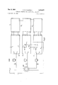
- FIGURE 1 is a schematic view of a two-phase inverting apparatus embodying the invention
- FIG. 2 is a view of a three-phase inverting apparatus embodying the network.
- FIG. 3 is a modified form of three-phase apparatus as shown in FIG. 2.
- the numeral 1 designates generally a two-phase inverting apparatus having a pair of single-phase inverters 2A and 2B driven respectively by a master oscillator 4 and a slave oscillator 4A.
- the inverters 2A and 2B are provided with input terminals 6 and 8 and output terminals 10 and 12.
- the oscillators derive their energy from a suitable source of unidirectional-potential electrical energy (not shown) which maintains a supply terminal 14 positive with respect to a supply terminal 16.
- the terminal Patented Dec. 6, 1966 14 is connnected through a disconnect switch 18 and an inductance 20 to the input terminal 6 of the inverter 2A.
- the terminal 8 of the inverter 2A is connected to the terminal 6 of the inverter 2B by a conductor 22 while the terminal 8 of the inverter 2B is connected by a conductor 24 to the negative supply terminal 16.
- the inverters 2A and 2B are identical and the details of only the inverter 2A is illustrated.
- Each inverter comprises a pair of current conducting paths interconnecting its input terminals 6 and 8 with the output terminals 10 and 12.
- the first path extends from the input terminal 6 through a first silicon controlled rectifier 26 to the output terminal 10 and from the output terminal 12 through a second silicon controlled rectifier 28 to the input terminal 8.
- the second current path extends from the input terminal 6 through a third silicon controlled rectifier 30 to the output terminal 12 and from the output terminal 10 through a fourth silicon controlled rectifier 32 to the input terminal 8.
- Each of the silicon controlled rectifiers or discontinuous control type electric valves 26, 28, 30 and 32 is provided with an anode a, a cathode c and a gate g and is rendered conducting anode a to cathode c by applying a pulse between the gate g and the cathode c in a direction to render the gate g positive with respect to the cathode c.
- the gates g and cathodes c of the valves commonly referred to as the control or pulsing circuit, are connected to individual secondary windings of a saturating core transformer through individual pulse producing networks 36.
- the pulsing circuits of the inverter 2A are energized from secondary windings of the transformer 34 of the master oscillator While those of the inverter 2B are energized from the secondary windings of the transformer 54 of the slave oscillator 4A.
- the networks 36 are arranged to provide a voltage wave of steep wave front to ensure the firing of the valves.
- the core of the transformers 34 and 54 are fabricated of iron having a substantially rectangular hysteresis loop.
- the transformer 34 of the master oscillator 4 is provided with a center tapped primary winding 38; the end terminals of which are connected to collectors c of transistors 40 and 42 and the center tap of which is connected to a negative power input terminal 48.
- the emitters e of these transistors 40 and 42 are connected to a common emitter bus 44 which is connected to the positive power input terminal 46.
- the base b of the transistor 40 is connected through a network 50 to the lower end terminal of the winding 38.
- the base b of the transistor 42 is connected through a second network 52 to the upper terminal of the primary winding 38.
- the oscillator 4 is self-oscillating. Since the transistors 40 and 42 are not absolutely identical in their leakage characteristics, one or the other thereof will commence to conduct more than the other thereof. Assuming that the transistor 40 has the greater leakage current, the leakage conduction will initiate a feedback potential to the base circuits which will cause the most conductive transistor 40 to become fully conducting and the other transistor 42 to be blocking. Transistor 40 continues to conduct until such time that the core of the transformer 34 saturates. When this occurs, the flux will cease to increase and the transistor 42 will no longer be driven nonconductive. When this occurs flux in the core 34 will decrease in magnitude from the saturated value to the remanence value inducing a voltage of opposite polarity in the winding 38.
- the voltages induced in the secondary windings are substantially rectangular in shape.
- the networks 36 transform these square wave pulses into peaked pulses which are applied in proper polarity to the silicon controlled rectifiers or valves 26 to 32. During one-half cycle of the output voltage of the oscillator 4 the produced pulses will render the valves 26 and 28 conducting and during the other half-cycle will render the valves 30 and 32 conducting.
- the corresponding valves of the inverter 2B are similarly connected to the secondary windings of the transformer 54 of the slave oscillator 4A through networks 36 identical t the networks 36 associated with the master oscillator 4.
- the transformer 54 is provided with a center tapped primary winding 56; the end terminals of which are connected to the collectors c of a pair of transistors 58 and 60 and the emitters e of which are connected through a common emitter bus 62 to a positive power input terminal 64.
- the negative input terminal 66 is directly connected to the center tap of the winding 56.
- the conduction of the transistors 58 and 60 is primary controlled by a feedback voltage derived from the secondary winding 68 and 70 of the transformer 54.
- the winding 68 is connected between the base b and the emitter e of the transistor 58 through a current limiting resistor 72 and the winding 70 is connected between the base b and emitter e of the transistor 60 through a current limiting resistor 74.
- resistor 80 The other of the resistor 80 is connected through a saturating core reactor 82 to one end of the resistance element of the potentiometer 78.
- the voltage appearing across the resistor 80 is applied to the slave oscillator by a pair of conductors 79 and 81 which connect end terminals of the resistor 80 between the bases In of the transistors 58 and 60.
- Prior to saturation of the reactor 82 insuflicient potential appears across the resistor 80 to influence operation of the slave oscillator 4A. However, when the react-or 82 saturates the potential appearing across the resistor 80 is suflicient to reverse operation of the slave oscillator 4A.
- the potentiometer 78 varies the voltage applied to the saturating reactor 82 and consequently the time interval between reversal of the polarity of the transformer 34 and the transmission of the reversing signal to the slave oscillator 4A for determining the phase difference of the out- .put voltages of-the inverters 2A and 2B.
- this time in- .terval would be 90 measured with respect to the output voltage of the transformer 34 or in the case of the three phase system as illustrated in FIGS. 2 and 3 the delay would be 120 electrical degrees.
- a two-phase induction motor 84 has one of its phases connected through a network 86 to the output terminals 1 and 12 of the inverter 2A while the other phase of the motor 84 is connected through a similar network 88 to the output terminals 10 and 12 of the inverter 28.
- networks 86 and 88 are necessary in view of the inductive characteristics of the motor 84. If the networks 86 and 88 were omitted the resultant voltage waveform across the commutating capacitors 90 would be an exponentially damped sinusoid, the natural frequency of which would be a function of the inductance of the inductor 20 and the capacity of the commutating capacitors 90 and the inductive characteristics of the load 84. If the natural frequency of the circuit just described is approximately the same as the operating frequency of the inverter, the capacitor voltage at the instant of commutation will be close to zero and the silicon controlled rectifiers cannot be shut off. If the natural frequency is greater than the operating frequency the capacitor voltage at the instant of commutation will be opposite to that required for shut 01f. On the other hand, if the natural frequency is approximately half or less of the operating frequency the voltage waveform across the capacitor will become triangular in shape. The system will operate in this case but the power handling capability of the system is seriously reduced and the load voltage waveform is very poor.
- the capacitor in shunt with the motor windings should be 50 microfarads, the inductance .195 millihenry and the capacitor in shunt circuit with the inductance of 15 microfarads.
- a shunting circuit is provided between the input terminals 6 and 8 of the inverter 2B.
- This shunting circuit comprises a resistor 92 and a momentary closure switch 94. With the switch 94 closed and pulses being applied by the master oscillator 4, one of the sets ofvalves 26-28 or 30-32 will receive a conducting pulse. When this occurs, current will flow from the supply terminal 14 through the now closed disconnect switch 18 and inductance 20 to the input terminal 6 of the inverter 2A. From terminal 6 the current will flow through the one of the sets of valves 26-28 or 30-32 which has received the conductive pulse.
- the conductive pulse is supplied to the rectifier valves 26 and 28 of the inverter 2A. These valves are consequently rendered conductive and current will flow from the input terminal 6 through the valve 26, the output terminal 10, the network 86, one-phase winding of the motor 84, the other output terminal 12, the valve 28, the input terminal 8 of inverter 2A, the input terminal 6 of the inverter 2B, the resistor 92, now closed switch 94, the terminal 8 of the inverter 2B, and conductor 24 to the negative terminal 16. Since the value of the resistor 92 is chosen so that at least a sustaining value of current will flow through the conducting valves 26 and 28 they will remain conducting when the firing pulse disappears and potential of a first polarity will continue to be supplied to the terminals 10 and 12.
- the slave oscillator 4A will supply conducting pulses to the corresponding valves 26 and 28 of the inverter 2B which become conducting since the voltage across the resistor 92 provides a sufficient potential across these valves.
- Current will now flow through the inverter 2B from its input terminal 6 through its valve 26, the network 88, the other phase winding of the motor 84, its other output terminal 12, its valve 28 back to its input terminal 8 and conductor 24 to the negative terminal 16 whereby potential of the first polarity -will continue to appear across its terminals and 12.
- the master oscillator 4 will render the valves and 32 of the inverter 2A conducting. Since the charge on the capacitor 90 cannot immediately change, the rendering of these valves conducting will raise the potential of the cathode of the associated valve 26 to a higher potential than that of the anode and this valve 26 will become extinguished. Similarly, the capacitor 90 will lower the potential of the anode of the associated valve 28 below that of its cathode and this valve 28 will become extinguished. The valves 30 and 32 will then continue to conduct and potential of a second polarity will be applied to the output terminals 10 and 12.
- the slave oscillator 4A will provide conducting pulses to the valves 30 and 32 of the inverter 2B whereby they conduct and the'commutating capacitor 90 of this inverter 2B will render its valves 26 and 23 blocking, as described above in connection with the inverter 2A, whereby potential of the second polarity will exist across its output terminals 1% and 12.
- the oscillator and master oscillator will continue to cause staggered pulses to be applied to the inverters 2A and 28 whereby two-phase alternating polarity output voltages appear at the output terminals 10 and 12 of these inverters.
- the switch 94 may be opened and preferably is opened as soon as possible after the inverter 23 cornmences to have its valves fired by the slave oscillator 4A.
- switch 94 is desirable so that during the majority of the operating time of the network It the resistor 92 is deenergized, it is appreciated that the switch 94 may be omitted and the resistor 92 maintained permanently connected between the terminals 6 and 8.
- Fig. 2 there is shown a modified form of the invention as applied to a three-phase inverter. It will be apparent that two of the inverters must be supplied with shunting networks so that they may be shunted to permit the unshunted one of the networks to have their electric valves fired. As illustrated the switch 194 sequentially opens the inverter 2B and 2C. While sequential opening is desirable and certain advantages are obtained thereby in its more generic form the switch 194 could open the shunting circuits substantially simultaneously. Again as in the two-phase system the switch 194 could be omitted entirely but in this instance again the etficiency would be reduced due to the continual energization of the shunting resistors 92.
- FIG. 3 also shows a three-phase system, however, in this instance it will be noted that two inverters 2B and 2C are shunted by the first shunting circuit which includes the resistor 292 and switch 294. The other of the inverters 2C is shunted by the resistor 292A which is connected through separate contacts on the switch 294.
- the switch 294 is shown as sequentially opening the shunting circuits and again certain advantages such as removal of shock to his system are obtained thereby, however, in its more generic form the switch 294 could simultaneously open the two shunting circuits or could be omitted entirely.
- N-1 shunting circuits may take the form as shown in FIG. 2 wherein each shunting circuit shunts a single inverter or may take the form as shown in FIG. 3 in which the first shunting circuits shunts N-l inverters, the second shunting circuit shunts N-Z inverters and so on down until the last or the N-lst shunting circuit shunts only a single inverter.
- an individual inverting apparatus for individually supplying each of the n phases of the system, a pair of supply terminals for energization from a unidirectional-potential electrical energy supply, means connecting said inverting apparatuses in series circuit between said supply terminals, and a unidirectional current con ducting shunting network connected in series with one of said inverting apparatuses and said supply terminals for conduction of current through said one inverting apparatus and between said supply terminals, said shunting network including n-l impedance elements connected in shunt with all of said apparatuses except said one apparatus.
- an individual inverting apparatus for individually supplying each of the n phases of the system, a pair of supply terminals for energization from a unidirectional-potential electrical energy supply, means connecting said inverting apparatuses in series circuit between said supply terminals, and a unidirectional current conducting shunting circuit including an impedance element, said shunting circuit being connected in shunt with at least one of said inverting apparatuses and in series with said supply terminals to conduct unidirectional current between said terminals.
- an individual inverting apparatus for individually supplying each of the n phases of the systern, a pair of supply terminals for energization from a unidirectional-potential electrical energy supply, means connecting said inverting apparatuses in series circuit between said supply terminals, 2, shunting network including n-l switches connected to shunt n1 of said inverting apparatuses, said shunting network being arranged such that progressive operation of said switches removes the shunt around a progressively increasing number of said n-l inverting apparatuses.
- an individual inverting apparatus for individually supplying each of the n phases of the system, a pair of supply terminals for energization from a unidirectional-potential electrical energy supply, means connecting said inverting apparatuses in series circuit between sai-d supply terminals, a shunting network including n-l switches and n-1 impedance elements connected to shunt n-l of said inverting apparatuses, said shunting network being arranged such that progressive operation of said switches progressively removes said impedance elements and removes the shunt around a progressively increasing number of said 11-1 inverting apparatuses.
- an individual inverting apparatus for individually supplying each of the n phases of the system, a pair of supply terminals for energization from a unidirectional-potential electrical energy supply, means connecting said inverting apparatuses in series circuit between said supply terminals, n-l shunting networks, means connecting a first of said shunting networks in shunt with n1 of said inverting apparatuses and a second of said shunting networks in shunt with 11-2 of said inverting apparatuses until all of said shunting networks are utilized, each said shunting network including an impedance device and a switch, means interconnecting said switch for sequential opening of said shunting circuits in the order named above.
- an individual inverting apparatus for individually supplying each of the n phases of the system, a pair of supply terminals for energization from a unidirectional-potential electrical energy supply, means connecting said inverting apparatuses in series circuit between said supply terminals, n-l shunting networks, each said network including an impedance element and a switch, and means individually connecting said shunting networks in shunt circuit with n-l of said inverting apparatuses.
- an individual inverting apparatus for individually supplying each of the n phases of the system, a pair of supply terminals for 'energization from a unidirectional-potential electrical energy supply, means connecting said inverting apparatuses in series circuit between said supply terminals, n1 shunting networks, each said network including an impedance element and a switch, means individually connecting said shunting networks in shunt circuit with n-l of said inverting apparatuses, and means interconnecting said switches for sequential operation.
- first and second inverting networks each said network having a pair of input terminals, a pair of output terminals, first and second discontinuous type valve devices, and first and second paths interconnecting said pairs of terminals; said first path including said first valve device and effective when said first valve device is conductive to energize said output terminals at a first polarity relative to said input terminals, said second path including said second valve device and efiective when said second valve device is conductive to energize said output terminals at a second polarity relative to said input terminals; firing means rendering said first valve devices conductive in sequence and said second valve devices conductive in sequence; a pair of supply terminals; means connecting said input terminals in series between said supply terminals; an impedance; and circuit means connecting said impedance across said input teraninals of one of said inverting networks for flow of unidirectional current therethrough between said pair of supply terminals and through one of said paths of the other of said inverting networks.
- first and second inverting networks each said network having a pair of input terminals, a pair of output terminals, first and second discontinuous type valve devices, and first and second paths interconnecting said pairs of terminals; said first path including said first valve device and effective when said first valve device is conductive to energize said output terminals at a first polarity relative to said input terminals, said second path including said second valve device and eifective when said second valve device is conductive to energize said output terminals at a second 'polarity relative to said input terminals; firing means rendering said first valve device conductive in sequence and said second valve devices conductive in sequence; a pair of supply terminals; means connecting said input terminals in series between said supply terminals; an impedance; a switch and means connecting said impedance in series with said switch across said input terminals of one of said inverting networks.
- first and second inverting networks each said network having a pair of input terminals, a pair of output terminals, a plurality of discontinuous type valve devices, and first and second paths interconnecting said pairs of terminals; said first path including a first and a second of said valve devices, said first paths being efiective when said first and second valve devices are conductive to energize said output terminals at a first polarity relative to said input terminals, said second path including a third and a fourth of said valve devices, said second path being effective when said third and said fourth valve devices are conductive to energize said output terminals at a second polarity relative to said input terminals, firing means rendering said first and second valve devices conductive substantially simultaneously and said third and fourth valve devices conductive substantially simultaneously; means for operating said firing means of said first network in staggered relation to said firing means of said second network; a pair of supply terminals; means connecting said input terminals in series between said supply terminals; an impedance; and means connecting said impedance across said
Landscapes
- Engineering & Computer Science (AREA)
- Power Engineering (AREA)
- Inverter Devices (AREA)
Description
STARTING APPARATUS FOR A MULTI-PHASE INVERTER Filed April 30, 1963 Dec. 6, 1966 v. c. SHANEMAN 5 Sheets-Sheet l INVENTOR Victor C. Shunemcm WITNESSES W fl Y/ ATTOR EY Dec. 6, 1966 v. c. SHANEMAN 3,290,577
STARTING APPARATUS FOR A MULTI-PHASE INVERTER Filed April 30, 1963 5 Sheets-Sheet 2 m g m "i g 8 g, 3 311 ME} as} n HH 2; W i\ STARTING APPARATUS FOR A MULTI-PHASE INVERTER Filed April 30, 1963 Dec. 6, 196 v. c. SHANEMAN 5 Sheets$heet 5 o o o u 0 JJ 0 Av o 0 NN 9 o n 0 w n n n o UHmM o o 0 o a a 0 o \mmm 0 0 0 0 b m o 0 O 0 o o u 0 a w o 0 0 United States Patent 3,290,577 STARTING APPARATUS FOR A MULTI- PHASE INVERTER Victor C. Shaneman, Shawnee Township, Allen County,
Ohio, assignor to Westinghouse Electric Corporation,
Pittsburgh, Pa., a corporation of Pennsylvania Filed Apr. 30, 1963, Ser. No. 276,726 10 Claims. (Cl. 321) This invention relates generally to multiphase inverting apparatus utilizing discontinuous type control valves and more particularly to means for starting such inverting apparatus.
In inverting apparatus utilizing discontinuous type control valves it is desirable from the standpoint of economy and the standpoint of overheating to fire the control valves with pulses of short duration. It will be appreciated that in a multi-phase inverter network the valves in one inverter will be rendered conductive at a time distinctly separate from the valves in any of the other inverters. Therefore, in starting a multi-phase inverter of this type, I propose to temporarily energize a shunt circuit around all except one of the inverters so that when a conducting pulse is applied to a control valve of the non-shunted inverter the control valve to which the pulse is applied will complete a circuit andbecome conductive. I further propose to provide impedance in such a shunting circuit so that sufiicient voltage is maintained across the terminals of the shunted inverters so that as their control valves are pulsed into conductive conditions they will also conduct. Thereafter, the shunting circuits may be opened and the control valves will be pulsed into conducting condition by the pulse source in the normal manner.
It is an object of this invention to provide an improved means for starting polyphase inverting apparatus of the series type.
It is a further object of this invention to provide in such an inverting apparatus shunting means for at least N-l of the inverters whereby the rendering of a control valve conductive will render it conducting.
Another object is to provide impedance means in such shunting circuit to limit the current flow through the conducting valve to a magnitude suflicient to maintain the discontinuous control valve conductive when the initiating pulse is discontinued.
A further object is to provide suflicient impedance in such shunting circuit to maintain suflicient voltage across the shunted inverters so that when its control valves are pulsed conductive these valves will also conduct.
Another object is to provide an improved method for operating the shunting circuits whereby they may be sequentially opened upon initiation of operation of the polyphase inverting apparatus.
Other objects will be apparent from the specification, the appended claims and the drawings, in which drawings:
FIGURE 1 is a schematic view of a two-phase inverting apparatus embodying the invention;
FIG. 2 is a view of a three-phase inverting apparatus embodying the network; and
FIG. 3 is a modified form of three-phase apparatus as shown in FIG. 2.
Referring to the drawings by characters of reference the numeral 1 designates generally a two-phase inverting apparatus having a pair of single- phase inverters 2A and 2B driven respectively by a master oscillator 4 and a slave oscillator 4A. The inverters 2A and 2B are provided with input terminals 6 and 8 and output terminals 10 and 12. The oscillators derive their energy from a suitable source of unidirectional-potential electrical energy (not shown) which maintains a supply terminal 14 positive with respect to a supply terminal 16. The terminal Patented Dec. 6, 1966 14 is connnected through a disconnect switch 18 and an inductance 20 to the input terminal 6 of the inverter 2A. The terminal 8 of the inverter 2A is connected to the terminal 6 of the inverter 2B by a conductor 22 while the terminal 8 of the inverter 2B is connected by a conductor 24 to the negative supply terminal 16.
The inverters 2A and 2B are identical and the details of only the inverter 2A is illustrated. Each inverter comprises a pair of current conducting paths interconnecting its input terminals 6 and 8 with the output terminals 10 and 12. The first path extends from the input terminal 6 through a first silicon controlled rectifier 26 to the output terminal 10 and from the output terminal 12 through a second silicon controlled rectifier 28 to the input terminal 8. Similarly, the second current path extends from the input terminal 6 through a third silicon controlled rectifier 30 to the output terminal 12 and from the output terminal 10 through a fourth silicon controlled rectifier 32 to the input terminal 8. Each of the silicon controlled rectifiers or discontinuous control type electric valves 26, 28, 30 and 32 is provided with an anode a, a cathode c and a gate g and is rendered conducting anode a to cathode c by applying a pulse between the gate g and the cathode c in a direction to render the gate g positive with respect to the cathode c. For this purpose the gates g and cathodes c of the valves, commonly referred to as the control or pulsing circuit, are connected to individual secondary windings of a saturating core transformer through individual pulse producing networks 36. The pulsing circuits of the inverter 2A are energized from secondary windings of the transformer 34 of the master oscillator While those of the inverter 2B are energized from the secondary windings of the transformer 54 of the slave oscillator 4A. The networks 36 are arranged to provide a voltage wave of steep wave front to ensure the firing of the valves.
Preferably, the core of the transformers 34 and 54 are fabricated of iron having a substantially rectangular hysteresis loop. The transformer 34 of the master oscillator 4 is provided with a center tapped primary winding 38; the end terminals of which are connected to collectors c of transistors 40 and 42 and the center tap of which is connected to a negative power input terminal 48. The emitters e of these transistors 40 and 42 are connected to a common emitter bus 44 which is connected to the positive power input terminal 46. The base b of the transistor 40 is connected through a network 50 to the lower end terminal of the winding 38. Likewise, the base b of the transistor 42 is connected through a second network 52 to the upper terminal of the primary winding 38. The oscillator 4 is self-oscillating. Since the transistors 40 and 42 are not absolutely identical in their leakage characteristics, one or the other thereof will commence to conduct more than the other thereof. Assuming that the transistor 40 has the greater leakage current, the leakage conduction will initiate a feedback potential to the base circuits which will cause the most conductive transistor 40 to become fully conducting and the other transistor 42 to be blocking. Transistor 40 continues to conduct until such time that the core of the transformer 34 saturates. When this occurs, the flux will cease to increase and the transistor 42 will no longer be driven nonconductive. When this occurs flux in the core 34 will decrease in magnitude from the saturated value to the remanence value inducing a voltage of opposite polarity in the winding 38. This will cause base drive current to flow in the transistor 42 initiating a regenerative action whereby the transistor 42 rapidly becomes fully conductive whereby current flows into the primary winding 38 in the opposite direction until it drives the core of the transformer 34 to saturation in the opposite direction. The master oscillator will continue to oscillate as above described thereby inducing an alternating voltage in the secondary windings of its transformer 34.
The voltages induced in the secondary windings are substantially rectangular in shape. The networks 36 transform these square wave pulses into peaked pulses which are applied in proper polarity to the silicon controlled rectifiers or valves 26 to 32. During one-half cycle of the output voltage of the oscillator 4 the produced pulses will render the valves 26 and 28 conducting and during the other half-cycle will render the valves 30 and 32 conducting.
The corresponding valves of the inverter 2B are similarly connected to the secondary windings of the transformer 54 of the slave oscillator 4A through networks 36 identical t the networks 36 associated with the master oscillator 4. The transformer 54 is provided with a center tapped primary winding 56; the end terminals of which are connected to the collectors c of a pair of transistors 58 and 60 and the emitters e of which are connected through a common emitter bus 62 to a positive power input terminal 64. The negative input terminal 66 is directly connected to the center tap of the winding 56. The conduction of the transistors 58 and 60 is primary controlled by a feedback voltage derived from the secondary winding 68 and 70 of the transformer 54. For
this purpose the winding 68 is connected between the base b and the emitter e of the transistor 58 through a current limiting resistor 72 and the winding 70 is connected between the base b and emitter e of the transistor 60 through a current limiting resistor 74.
The potentiometer 78 varies the voltage applied to the saturating reactor 82 and consequently the time interval between reversal of the polarity of the transformer 34 and the transmission of the reversing signal to the slave oscillator 4A for determining the phase difference of the out- .put voltages of-the inverters 2A and 2B. In the case of the two-phase system, as shown in FIG. 1, this time in- .terval would be 90 measured with respect to the output voltage of the transformer 34 or in the case of the three phase system as illustrated in FIGS. 2 and 3 the delay would be 120 electrical degrees.
A two-phase induction motor 84 has one of its phases connected through a network 86 to the output terminals 1 and 12 of the inverter 2A while the other phase of the motor 84 is connected through a similar network 88 to the output terminals 10 and 12 of the inverter 28. The
Proper selection of the values of the network components eliminates most of these problems and they may be selected so that sinusoidal waveforms of voltage and current will be applied to the motor 84. Assuming a motor which has at standstill an effective resistive impedance of .32 ohm and an inductive impedance of .78 ohm and at full speed has a resistive impedance of 3.45 ohms and an inductive impedance of 2.26 ohms and a filter capacitor of 75 microfarads, the capacitor in shunt with the motor windings should be 50 microfarads, the inductance .195 millihenry and the capacitor in shunt circuit with the inductance of 15 microfarads.
It is believed that the remainder of the description may best be set forth by a description of operation which is as follows: Upon closure of the disconnect switch 18, voltage from the power supply terminals 14 and 16 is applied through the inductance or constant current device 20 between the input terminal 6 of the inverter 2A and the input terminal 8 of the inverter 2B. If, at the same time, a potential is supplied to the terminals 46 and 48 of the master oscillator and 64 and 66 of the slave oscillator, firing pulses will be applied to the silicon controlled rec- 'tifiers of the inverters 2A and 2B. These inverters will not immediately commence to conduct because of the sequence at which the pulses are supplied thereto; the pulses supplied to the inverter 2A occurring at intervals when no pulses are supplied to the inverter 2B.
In order that the valves 26-28 or 30-32 may become conductive when pulses are applied thereto from the master oscillator 4, a shunting circuit is provided between the input terminals 6 and 8 of the inverter 2B. This shunting circuit comprises a resistor 92 and a momentary closure switch 94. With the switch 94 closed and pulses being applied by the master oscillator 4, one of the sets ofvalves 26-28 or 30-32 will receive a conducting pulse. When this occurs, current will flow from the supply terminal 14 through the now closed disconnect switch 18 and inductance 20 to the input terminal 6 of the inverter 2A. From terminal 6 the current will flow through the one of the sets of valves 26-28 or 30-32 which has received the conductive pulse. For purposes of explanation assume that the conductive pulse is supplied to the rectifier valves 26 and 28 of the inverter 2A. These valves are consequently rendered conductive and current will flow from the input terminal 6 through the valve 26, the output terminal 10, the network 86, one-phase winding of the motor 84, the other output terminal 12, the valve 28, the input terminal 8 of inverter 2A, the input terminal 6 of the inverter 2B, the resistor 92, now closed switch 94, the terminal 8 of the inverter 2B, and conductor 24 to the negative terminal 16. Since the value of the resistor 92 is chosen so that at least a sustaining value of current will flow through the conducting valves 26 and 28 they will remain conducting when the firing pulse disappears and potential of a first polarity will continue to be supplied to the terminals 10 and 12.
Subsequently the slave oscillator 4A will supply conducting pulses to the corresponding valves 26 and 28 of the inverter 2B which become conducting since the voltage across the resistor 92 provides a sufficient potential across these valves. Current will now flow through the inverter 2B from its input terminal 6 through its valve 26, the network 88, the other phase winding of the motor 84, its other output terminal 12, its valve 28 back to its input terminal 8 and conductor 24 to the negative terminal 16 whereby potential of the first polarity -will continue to appear across its terminals and 12.
One hundred eighty degrees after firing of the valves 26 and 28, the master oscillator 4 will render the valves and 32 of the inverter 2A conducting. Since the charge on the capacitor 90 cannot immediately change, the rendering of these valves conducting will raise the potential of the cathode of the associated valve 26 to a higher potential than that of the anode and this valve 26 will become extinguished. Similarly, the capacitor 90 will lower the potential of the anode of the associated valve 28 below that of its cathode and this valve 28 will become extinguished. The valves 30 and 32 will then continue to conduct and potential of a second polarity will be applied to the output terminals 10 and 12. Ninety degrees later or 270 after initial firing of the valves 26 and 28 of the inverter 2A, the slave oscillator 4A will provide conducting pulses to the valves 30 and 32 of the inverter 2B whereby they conduct and the'commutating capacitor 90 of this inverter 2B will render its valves 26 and 23 blocking, as described above in connection with the inverter 2A, whereby potential of the second polarity will exist across its output terminals 1% and 12.
The oscillator and master oscillator will continue to cause staggered pulses to be applied to the inverters 2A and 28 whereby two-phase alternating polarity output voltages appear at the output terminals 10 and 12 of these inverters. The switch 94 may be opened and preferably is opened as soon as possible after the inverter 23 cornmences to have its valves fired by the slave oscillator 4A.
While the switch 94 is desirable so that during the majority of the operating time of the network It the resistor 92 is deenergized, it is appreciated that the switch 94 may be omitted and the resistor 92 maintained permanently connected between the terminals 6 and 8.
In Fig. 2 there is shown a modified form of the invention as applied to a three-phase inverter. It will be apparent that two of the inverters must be supplied with shunting networks so that they may be shunted to permit the unshunted one of the networks to have their electric valves fired. As illustrated the switch 194 sequentially opens the inverter 2B and 2C. While sequential opening is desirable and certain advantages are obtained thereby in its more generic form the switch 194 could open the shunting circuits substantially simultaneously. Again as in the two-phase system the switch 194 could be omitted entirely but in this instance again the etficiency would be reduced due to the continual energization of the shunting resistors 92.
FIG. 3 also shows a three-phase system, however, in this instance it will be noted that two inverters 2B and 2C are shunted by the first shunting circuit which includes the resistor 292 and switch 294. The other of the inverters 2C is shunted by the resistor 292A which is connected through separate contacts on the switch 294. Again the switch 294 is shown as sequentially opening the shunting circuits and again certain advantages such as removal of shock to his system are obtained thereby, however, in its more generic form the switch 294 could simultaneously open the two shunting circuits or could be omitted entirely.
From the foregoing it will be seen that the number of phases and consequently the number of single-phase producing inverter apparatuses is immaterial, however, it is apparent that when the inverter network supplies a source having N phases there need to be N-1 shunting circuits. These may take the form as shown in FIG. 2 wherein each shunting circuit shunts a single inverter or may take the form as shown in FIG. 3 in which the first shunting circuits shunts N-l inverters, the second shunting circuit shunts N-Z inverters and so on down until the last or the N-lst shunting circuit shunts only a single inverter.
While only a limited number of embodiments of the invention have been shown, it will be appreciated that many modifications may be made thereto and still come within the scope of the appended claims.
What is claimed and is desired to be secured by United States Letters Patent is as follows:
1. In an inverting system for energizing a polyphase network of n phases, an individual inverting apparatus for individually supplying each of the n phases of the system, a pair of supply terminals for energization from a unidirectional-potential electrical energy supply, means connecting said inverting apparatuses in series circuit between said supply terminals, and a unidirectional current con ducting shunting network connected in series with one of said inverting apparatuses and said supply terminals for conduction of current through said one inverting apparatus and between said supply terminals, said shunting network including n-l impedance elements connected in shunt with all of said apparatuses except said one apparatus.
2. In an inverting system for energizing a polyphase network of at least two phases, an individual inverting apparatus for individually supplying each of the n phases of the system, a pair of supply terminals for energization from a unidirectional-potential electrical energy supply, means connecting said inverting apparatuses in series circuit between said supply terminals, and a unidirectional current conducting shunting circuit including an impedance element, said shunting circuit being connected in shunt with at least one of said inverting apparatuses and in series with said supply terminals to conduct unidirectional current between said terminals.
3. In an inverting system for energizing a polyphase network of n phases, an individual inverting apparatus for individually supplying each of the n phases of the systern, a pair of supply terminals for energization from a unidirectional-potential electrical energy supply, means connecting said inverting apparatuses in series circuit between said supply terminals, 2, shunting network including n-l switches connected to shunt n1 of said inverting apparatuses, said shunting network being arranged such that progressive operation of said switches removes the shunt around a progressively increasing number of said n-l inverting apparatuses.
4. In an inverting system for energizing a polyphase network of n phases, an individual inverting apparatus for individually supplying each of the n phases of the system, a pair of supply terminals for energization from a unidirectional-potential electrical energy supply, means connecting said inverting apparatuses in series circuit between sai-d supply terminals, a shunting network including n-l switches and n-1 impedance elements connected to shunt n-l of said inverting apparatuses, said shunting network being arranged such that progressive operation of said switches progressively removes said impedance elements and removes the shunt around a progressively increasing number of said 11-1 inverting apparatuses.
5. In an inverting system for energizing a polyphase network of n phases, an individual inverting apparatus for individually supplying each of the n phases of the system, a pair of supply terminals for energization from a unidirectional-potential electrical energy supply, means connecting said inverting apparatuses in series circuit between said supply terminals, n-l shunting networks, means connecting a first of said shunting networks in shunt with n1 of said inverting apparatuses and a second of said shunting networks in shunt with 11-2 of said inverting apparatuses until all of said shunting networks are utilized, each said shunting network including an impedance device and a switch, means interconnecting said switch for sequential opening of said shunting circuits in the order named above.
I 6. In an inverting system for energizing a polyphase network of n phases, an individual inverting apparatus for individually supplying each of the n phases of the system, a pair of supply terminals for energization from a unidirectional-potential electrical energy supply, means connecting said inverting apparatuses in series circuit between said supply terminals, n-l shunting networks, each said network including an impedance element and a switch, and means individually connecting said shunting networks in shunt circuit with n-l of said inverting apparatuses.
7. In an inverting system for energizing a polyphase network of n phases, an individual inverting apparatus for individually supplying each of the n phases of the system, a pair of supply terminals for 'energization from a unidirectional-potential electrical energy supply, means connecting said inverting apparatuses in series circuit between said supply terminals, n1 shunting networks, each said network including an impedance element and a switch, means individually connecting said shunting networks in shunt circuit with n-l of said inverting apparatuses, and means interconnecting said switches for sequential operation.
8. In an inverting system; first and second inverting networks; each said network having a pair of input terminals, a pair of output terminals, first and second discontinuous type valve devices, and first and second paths interconnecting said pairs of terminals; said first path including said first valve device and effective when said first valve device is conductive to energize said output terminals at a first polarity relative to said input terminals, said second path including said second valve device and efiective when said second valve device is conductive to energize said output terminals at a second polarity relative to said input terminals; firing means rendering said first valve devices conductive in sequence and said second valve devices conductive in sequence; a pair of supply terminals; means connecting said input terminals in series between said supply terminals; an impedance; and circuit means connecting said impedance across said input teraninals of one of said inverting networks for flow of unidirectional current therethrough between said pair of supply terminals and through one of said paths of the other of said inverting networks.
9. In an inverting system; first and second inverting networks; each said network having a pair of input terminals, a pair of output terminals, first and second discontinuous type valve devices, and first and second paths interconnecting said pairs of terminals; said first path including said first valve device and effective when said first valve device is conductive to energize said output terminals at a first polarity relative to said input terminals, said second path including said second valve device and eifective when said second valve device is conductive to energize said output terminals at a second 'polarity relative to said input terminals; firing means rendering said first valve device conductive in sequence and said second valve devices conductive in sequence; a pair of supply terminals; means connecting said input terminals in series between said supply terminals; an impedance; a switch and means connecting said impedance in series with said switch across said input terminals of one of said inverting networks.
11 In an inverting system; first and second inverting networks; each said network having a pair of input terminals, a pair of output terminals, a plurality of discontinuous type valve devices, and first and second paths interconnecting said pairs of terminals; said first path including a first and a second of said valve devices, said first paths being efiective when said first and second valve devices are conductive to energize said output terminals at a first polarity relative to said input terminals, said second path including a third and a fourth of said valve devices, said second path being effective when said third and said fourth valve devices are conductive to energize said output terminals at a second polarity relative to said input terminals, firing means rendering said first and second valve devices conductive substantially simultaneously and said third and fourth valve devices conductive substantially simultaneously; means for operating said firing means of said first network in staggered relation to said firing means of said second network; a pair of supply terminals; means connecting said input terminals in series between said supply terminals; an impedance; and means connecting said impedance across said input terminals of one of said inverting networks.
References Cited by the Examiner UNITED STATES PATENTS 3,175,167 3/1965 Lloyd 318-431 X FOREIGN PATENTS 243,568 2/ 1963 Australia.
JOHN F. COUCH, Primary Examiner.
W. H. BEHA, Assistant Examiner.
Claims (1)
1. IN AN INVERTING SYSTEM FOR ENERGIZING A POLYPHASE NETWORK OF N PHASES, AN INDIVIDUAL INVERTING APPARATUS FOR INDIVIDUALLY SUPPLYING EACH OF THE N PHASES OF THE SYSTEM, A PAIR OF SUPPLY TERMINALS FOR ENERGIZATION FROM A UNIDIRECTIONAL-POTENTIAL ELECTRICAL ENERGY SUPPLY, MEANS CONNECTING SAID INVERTING APPARATUSES IN SERIES CIRCUIT BETWEEN SAID SUPPLY TERMINALS, AND A UNIDIRECTIONAL CURRENT CONDUCTING SHUNTING NETWORK CONNECTED IN SERIES WITH ONE OF SAID INVERTING APPARATUSES AND SAID SUPPLY TERMINALS FOR CONDUCTION OF CURRENT THROUGH SAID ONE INVERTING APPARATUS AND BETWEEN SAID SUPPLY TERMINALS, SAID SHUNTING NETWORK INCLUDING N-1 IMPEDANCE ELEMENTS CONNECTED IN SHUNT WITH ALL OF SAID APPARATUSES EXCEPT SAID ONE APPARATUS.
Priority Applications (1)
| Application Number | Priority Date | Filing Date | Title |
|---|---|---|---|
| US276726A US3290577A (en) | 1963-04-30 | 1963-04-30 | Starting apparatus for a multiphase inverter |
Applications Claiming Priority (1)
| Application Number | Priority Date | Filing Date | Title |
|---|---|---|---|
| US276726A US3290577A (en) | 1963-04-30 | 1963-04-30 | Starting apparatus for a multiphase inverter |
Publications (1)
| Publication Number | Publication Date |
|---|---|
| US3290577A true US3290577A (en) | 1966-12-06 |
Family
ID=23057842
Family Applications (1)
| Application Number | Title | Priority Date | Filing Date |
|---|---|---|---|
| US276726A Expired - Lifetime US3290577A (en) | 1963-04-30 | 1963-04-30 | Starting apparatus for a multiphase inverter |
Country Status (1)
| Country | Link |
|---|---|
| US (1) | US3290577A (en) |
Cited By (1)
| Publication number | Priority date | Publication date | Assignee | Title |
|---|---|---|---|---|
| JPS5271655A (en) * | 1975-12-11 | 1977-06-15 | Tdk Corp | Control system in power supply circuit |
Citations (1)
| Publication number | Priority date | Publication date | Assignee | Title |
|---|---|---|---|---|
| US3175167A (en) * | 1961-07-27 | 1965-03-23 | Gen Mills Inc | Direct-current to alternating-current saturable core inverters |
-
1963
- 1963-04-30 US US276726A patent/US3290577A/en not_active Expired - Lifetime
Patent Citations (1)
| Publication number | Priority date | Publication date | Assignee | Title |
|---|---|---|---|---|
| US3175167A (en) * | 1961-07-27 | 1965-03-23 | Gen Mills Inc | Direct-current to alternating-current saturable core inverters |
Cited By (1)
| Publication number | Priority date | Publication date | Assignee | Title |
|---|---|---|---|---|
| JPS5271655A (en) * | 1975-12-11 | 1977-06-15 | Tdk Corp | Control system in power supply circuit |
Similar Documents
| Publication | Publication Date | Title |
|---|---|---|
| US3120633A (en) | Series inverter circuit having controlled rectifiers with power diodes in reverse parallel connection | |
| US3207974A (en) | Inverter circuits | |
| US3120634A (en) | Controlled rectifier inverter circuit | |
| US3257604A (en) | Inverter | |
| JPH10506260A (en) | High-voltage DC power transmission system | |
| US3219905A (en) | Method of obtaining artificial commutation of an inverter | |
| US3222587A (en) | Alternating current converting circuit | |
| US4092510A (en) | Multiple-load induction heating cooking apparatus with means for eliminating interference between two or more commutation circuits | |
| US3648149A (en) | Polyphase inverter circuit | |
| US3242415A (en) | Inverters | |
| US2306230A (en) | Electric valve translating system | |
| US3390320A (en) | Transistor inverter for synchronized operation with a like paralleled inverter | |
| US3321693A (en) | Inverter and switching scheme therefor | |
| US3718853A (en) | Pulse width limiting means for inverter circuits | |
| US3341737A (en) | Constant current supply especially for fluorescent lamps | |
| US3320514A (en) | Circuit means for selectively switching current-conducting groups of a cycloconverter in response to output current | |
| US2265717A (en) | Electric translating apparatus | |
| US3059191A (en) | Inverter network | |
| US3992638A (en) | Synchronous switch | |
| US3413539A (en) | Direct current-alternating current inverters having a pair of controlled rectifiers | |
| US3469169A (en) | Inverter apparatus | |
| US3290577A (en) | Starting apparatus for a multiphase inverter | |
| US3331011A (en) | Inverter control means | |
| US3302093A (en) | Electric frequency changers | |
| US3504264A (en) | Variable duty cycle switching apparatus |