US3290558A - Mounting arrangement for unidirectionally conductive devices - Google Patents
Mounting arrangement for unidirectionally conductive devices Download PDFInfo
- Publication number
- US3290558A US3290558A US341082A US34108264A US3290558A US 3290558 A US3290558 A US 3290558A US 341082 A US341082 A US 341082A US 34108264 A US34108264 A US 34108264A US 3290558 A US3290558 A US 3290558A
- Authority
- US
- United States
- Prior art keywords
- conductor
- faces
- openings
- face
- diode
- Prior art date
- Legal status (The legal status is an assumption and is not a legal conclusion. Google has not performed a legal analysis and makes no representation as to the accuracy of the status listed.)
- Expired - Lifetime
Links
Images
Classifications
-
- H—ELECTRICITY
- H05—ELECTRIC TECHNIQUES NOT OTHERWISE PROVIDED FOR
- H05K—PRINTED CIRCUITS; CASINGS OR CONSTRUCTIONAL DETAILS OF ELECTRIC APPARATUS; MANUFACTURE OF ASSEMBLAGES OF ELECTRICAL COMPONENTS
- H05K1/00—Printed circuits
- H05K1/18—Printed circuits structurally associated with non-printed electric components
- H05K1/182—Printed circuits structurally associated with non-printed electric components associated with components mounted in the printed circuit board, e.g. insert mounted components [IMC]
- H05K1/184—Components including terminals inserted in holes through the printed circuit board and connected to printed contacts on the walls of the holes or at the edges thereof or protruding over or into the holes
-
- H—ELECTRICITY
- H01—ELECTRIC ELEMENTS
- H01L—SEMICONDUCTOR DEVICES NOT COVERED BY CLASS H10
- H01L25/00—Assemblies consisting of a plurality of individual semiconductor or other solid state devices ; Multistep manufacturing processes thereof
- H01L25/03—Assemblies consisting of a plurality of individual semiconductor or other solid state devices ; Multistep manufacturing processes thereof all the devices being of a type provided for in the same subgroup of groups H01L27/00 - H01L33/00, or in a single subclass of H10K, H10N, e.g. assemblies of rectifier diodes
-
- H—ELECTRICITY
- H05—ELECTRIC TECHNIQUES NOT OTHERWISE PROVIDED FOR
- H05K—PRINTED CIRCUITS; CASINGS OR CONSTRUCTIONAL DETAILS OF ELECTRIC APPARATUS; MANUFACTURE OF ASSEMBLAGES OF ELECTRICAL COMPONENTS
- H05K1/00—Printed circuits
- H05K1/02—Details
- H05K1/0286—Programmable, customizable or modifiable circuits
- H05K1/0287—Programmable, customizable or modifiable circuits having an universal lay-out, e.g. pad or land grid patterns or mesh patterns
- H05K1/0289—Programmable, customizable or modifiable circuits having an universal lay-out, e.g. pad or land grid patterns or mesh patterns having a matrix lay-out, i.e. having selectively interconnectable sets of X-conductors and Y-conductors in different planes
-
- H—ELECTRICITY
- H05—ELECTRIC TECHNIQUES NOT OTHERWISE PROVIDED FOR
- H05K—PRINTED CIRCUITS; CASINGS OR CONSTRUCTIONAL DETAILS OF ELECTRIC APPARATUS; MANUFACTURE OF ASSEMBLAGES OF ELECTRICAL COMPONENTS
- H05K1/00—Printed circuits
- H05K1/18—Printed circuits structurally associated with non-printed electric components
- H05K1/182—Printed circuits structurally associated with non-printed electric components associated with components mounted in the printed circuit board, e.g. insert mounted components [IMC]
- H05K1/183—Components mounted in and supported by recessed areas of the printed circuit board
-
- H—ELECTRICITY
- H01—ELECTRIC ELEMENTS
- H01L—SEMICONDUCTOR DEVICES NOT COVERED BY CLASS H10
- H01L2924/00—Indexing scheme for arrangements or methods for connecting or disconnecting semiconductor or solid-state bodies as covered by H01L24/00
- H01L2924/0001—Technical content checked by a classifier
- H01L2924/0002—Not covered by any one of groups H01L24/00, H01L24/00 and H01L2224/00
-
- H—ELECTRICITY
- H05—ELECTRIC TECHNIQUES NOT OTHERWISE PROVIDED FOR
- H05K—PRINTED CIRCUITS; CASINGS OR CONSTRUCTIONAL DETAILS OF ELECTRIC APPARATUS; MANUFACTURE OF ASSEMBLAGES OF ELECTRICAL COMPONENTS
- H05K2201/00—Indexing scheme relating to printed circuits covered by H05K1/00
- H05K2201/09—Shape and layout
- H05K2201/09009—Substrate related
- H05K2201/09063—Holes or slots in insulating substrate not used for electrical connections
-
- H—ELECTRICITY
- H05—ELECTRIC TECHNIQUES NOT OTHERWISE PROVIDED FOR
- H05K—PRINTED CIRCUITS; CASINGS OR CONSTRUCTIONAL DETAILS OF ELECTRIC APPARATUS; MANUFACTURE OF ASSEMBLAGES OF ELECTRICAL COMPONENTS
- H05K2201/00—Indexing scheme relating to printed circuits covered by H05K1/00
- H05K2201/09—Shape and layout
- H05K2201/09818—Shape or layout details not covered by a single group of H05K2201/09009 - H05K2201/09809
- H05K2201/09845—Stepped hole, via, edge, bump or conductor
-
- H—ELECTRICITY
- H05—ELECTRIC TECHNIQUES NOT OTHERWISE PROVIDED FOR
- H05K—PRINTED CIRCUITS; CASINGS OR CONSTRUCTIONAL DETAILS OF ELECTRIC APPARATUS; MANUFACTURE OF ASSEMBLAGES OF ELECTRICAL COMPONENTS
- H05K2201/00—Indexing scheme relating to printed circuits covered by H05K1/00
- H05K2201/10—Details of components or other objects attached to or integrated in a printed circuit board
- H05K2201/10007—Types of components
- H05K2201/10174—Diode
-
- H—ELECTRICITY
- H05—ELECTRIC TECHNIQUES NOT OTHERWISE PROVIDED FOR
- H05K—PRINTED CIRCUITS; CASINGS OR CONSTRUCTIONAL DETAILS OF ELECTRIC APPARATUS; MANUFACTURE OF ASSEMBLAGES OF ELECTRICAL COMPONENTS
- H05K3/00—Apparatus or processes for manufacturing printed circuits
- H05K3/40—Forming printed elements for providing electric connections to or between printed circuits
- H05K3/4038—Through-connections; Vertical interconnect access [VIA] connections
- H05K3/4046—Through-connections; Vertical interconnect access [VIA] connections using auxiliary conductive elements, e.g. metallic spheres, eyelets, pieces of wire
-
- Y—GENERAL TAGGING OF NEW TECHNOLOGICAL DEVELOPMENTS; GENERAL TAGGING OF CROSS-SECTIONAL TECHNOLOGIES SPANNING OVER SEVERAL SECTIONS OF THE IPC; TECHNICAL SUBJECTS COVERED BY FORMER USPC CROSS-REFERENCE ART COLLECTIONS [XRACs] AND DIGESTS
- Y10—TECHNICAL SUBJECTS COVERED BY FORMER USPC
- Y10S—TECHNICAL SUBJECTS COVERED BY FORMER USPC CROSS-REFERENCE ART COLLECTIONS [XRACs] AND DIGESTS
- Y10S257/00—Active solid-state devices, e.g. transistors, solid-state diodes
- Y10S257/926—Elongated lead extending axially through another elongated lead
Definitions
- Electronic calculating machines and computers employ large numbers of diodes which are connected with each other and with other circuit elements by conductors.
- the bulk of conventionally arranged diodes and conductors results in the use of relatively long conductors which not only occupy a substantial amount of space, but are also undesirable as such, particularly in circuits operating at very high frequencies.
- An important object of the invention is the provision of a mounting arrangement in which a large number of diodes and the associated conductors are arranged in a minimum of space, thereby not only shortening the conductors, but also simplifying the construction of the apparatus of which the diodes constitute important parts.
- Another object is the provision of a mounting arrangementwhich is simpler to assemble, and therefore more economical than corresponding conventional devices, yet provides more reliable connections.
- a more specific object of the invention is the provision of uniform networks of conductively connected diodes which are suitable for stacking in module assemblies.
- the invention in one of its aspects provides a sheet member of electrically insulating material having two opposite faces.
- the sheet member is formed with a plurality of spaced openings which extend from one face to the other.
- a diode is arranged in each aperture and its two leads project therefrom in opposite directions.
- the two faces of the sheet member carry respective electric circuits, and the leads of the diodes are conductively connected to the circuits.
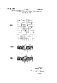
- FIG. 1 diagrammatically illustrates a diode assembly of the invention
- FIG. 2 shows a detail of the assembly of FIG. 1 in 'elevational section, a diode being removed to reveal other features of the device;
- FIG. 3 shows the device of FIG. 2 with a diode in place.
- FIG. 1 there is shown a matrix arrangement of ten parallel conductors 2 evenly spaced in a common plane and of eight conductors 3 parallel to each other, perpendicular to the conductors 2, and evenly spaced in a comm-on plane. Twelve diodes 8 are distributed over the matrix of conductors 2, 3 in a pattern not in itself relevant to this invention. Each diode 8 connects a conductor 2 to a conductor 3 for flow of current from the former to the latter.
- the sheet 1 is perforated.
- Each opening in the sheet 1 has a wider axial portion 4 and a narrower axial portion 5.
- the two portions are mainly cylindrical, but the innermost part of the opening portion 4 tapers conically toward the narrower portion 5.
- the openings are arranged in the sheet 1 in a regular pattern, evident from FIG. 1, wherever conductors 2 and 3 intersect and are separated from each other by the thickness of the sheet only.
- a diode may be inserted into each wider opening portion 4 in such a manner that the two leads 6, 7 of the diode axially extend in opposite directions outward of the orifices of the opening for contact with the conductors 2 and 3 respectively.
- the conductors 2 and 3 on the two faces of the sheet 1 may be formed by any conventional process known in the art of printed circuits. They may be elements of a copper foil shaped by die cutting or etching, or they may consist of electrodeposited copper or other conductive metal electrolytically precipitated on a printed pattern of conductive silver paste in the usual manner.
- a diode mounting arrangement comprising, in combination:
- each conductor means including a plurality of conductor members elongated in a common direction and spaced from each other transversely of said common direction,
Applications Claiming Priority (1)
| Application Number | Priority Date | Filing Date | Title |
|---|---|---|---|
| FR923527A FR1355034A (fr) | 1963-02-01 | 1963-02-01 | Nouveau mode de construction d'ensembles comportant des éléments à conductibilité asymétrique et analogues |
Publications (1)
| Publication Number | Publication Date |
|---|---|
| US3290558A true US3290558A (en) | 1966-12-06 |
Family
ID=8796148
Family Applications (1)
| Application Number | Title | Priority Date | Filing Date |
|---|---|---|---|
| US341082A Expired - Lifetime US3290558A (en) | 1963-02-01 | 1964-01-29 | Mounting arrangement for unidirectionally conductive devices |
Country Status (4)
| Country | Link |
|---|---|
| US (1) | US3290558A (fr) |
| DE (1) | DE1464823A1 (fr) |
| FR (1) | FR1355034A (fr) |
| GB (1) | GB1035722A (fr) |
Cited By (9)
| Publication number | Priority date | Publication date | Assignee | Title |
|---|---|---|---|---|
| US3529097A (en) * | 1964-07-24 | 1970-09-15 | Itt | Homogeneous matrix switching network |
| US3539873A (en) * | 1967-10-19 | 1970-11-10 | Clare & Co C P | Matrix board apparatus |
| US3731015A (en) * | 1971-05-18 | 1973-05-01 | Universal Technology | Control keyboard switch with cantilevered contact and diode matrix array |
| US4086426A (en) * | 1976-07-01 | 1978-04-25 | Motorola Inc. | Stress relieved printed wiring board |
| WO1980001860A1 (fr) * | 1979-03-01 | 1980-09-04 | Amp Inc | Panneau d'affichage a diodes emettrices de lumiere |
| WO1985005733A1 (fr) * | 1984-05-30 | 1985-12-19 | Motorola, Inc. | Assemblage de modules a circuit integre de densite elevee |
| US4646204A (en) * | 1986-02-10 | 1987-02-24 | Rca Corporation | Hole geometry for printed circuit boards |
| US4829404A (en) * | 1987-04-27 | 1989-05-09 | Flexmark, Inc. | Method of producing a flexible circuit and master grid therefor |
| US20150014034A1 (en) * | 2013-07-15 | 2015-01-15 | Samsung Electro-Mechanics Co., Ltd. | Printed circuit board having embedded electronic device and method of manufacturing the same |
Families Citing this family (1)
| Publication number | Priority date | Publication date | Assignee | Title |
|---|---|---|---|---|
| FR2301952A1 (fr) * | 1975-02-22 | 1976-09-17 | Lucas Industries Ltd | Machine electrique rotative sans balai |
Citations (5)
| Publication number | Priority date | Publication date | Assignee | Title |
|---|---|---|---|---|
| US2902628A (en) * | 1951-09-14 | 1959-09-01 | Int Standard Electric Corp | Terminal assembly with cells for electrical components |
| US2911605A (en) * | 1956-10-02 | 1959-11-03 | Monroe Calculating Machine | Printed circuitry |
| US3105729A (en) * | 1960-04-01 | 1963-10-01 | Rosenthal Herbert | Electrical connecting apparatus |
| US3142783A (en) * | 1959-12-22 | 1964-07-28 | Hughes Aircraft Co | Electrical circuit system |
| US3158927A (en) * | 1961-06-05 | 1964-12-01 | Burroughs Corp | Method of fabricating sub-miniature semiconductor matrix apparatus |
-
1963
- 1963-02-01 FR FR923527A patent/FR1355034A/fr not_active Expired
-
1964
- 1964-01-29 GB GB3885/64A patent/GB1035722A/en not_active Expired
- 1964-01-29 US US341082A patent/US3290558A/en not_active Expired - Lifetime
- 1964-01-31 DE DE19641464823 patent/DE1464823A1/de active Pending
Patent Citations (5)
| Publication number | Priority date | Publication date | Assignee | Title |
|---|---|---|---|---|
| US2902628A (en) * | 1951-09-14 | 1959-09-01 | Int Standard Electric Corp | Terminal assembly with cells for electrical components |
| US2911605A (en) * | 1956-10-02 | 1959-11-03 | Monroe Calculating Machine | Printed circuitry |
| US3142783A (en) * | 1959-12-22 | 1964-07-28 | Hughes Aircraft Co | Electrical circuit system |
| US3105729A (en) * | 1960-04-01 | 1963-10-01 | Rosenthal Herbert | Electrical connecting apparatus |
| US3158927A (en) * | 1961-06-05 | 1964-12-01 | Burroughs Corp | Method of fabricating sub-miniature semiconductor matrix apparatus |
Cited By (11)
| Publication number | Priority date | Publication date | Assignee | Title |
|---|---|---|---|---|
| US3529097A (en) * | 1964-07-24 | 1970-09-15 | Itt | Homogeneous matrix switching network |
| US3539873A (en) * | 1967-10-19 | 1970-11-10 | Clare & Co C P | Matrix board apparatus |
| US3731015A (en) * | 1971-05-18 | 1973-05-01 | Universal Technology | Control keyboard switch with cantilevered contact and diode matrix array |
| US4086426A (en) * | 1976-07-01 | 1978-04-25 | Motorola Inc. | Stress relieved printed wiring board |
| WO1980001860A1 (fr) * | 1979-03-01 | 1980-09-04 | Amp Inc | Panneau d'affichage a diodes emettrices de lumiere |
| US4241277A (en) * | 1979-03-01 | 1980-12-23 | Amp Incorporated | LED Display panel having bus conductors on flexible support |
| WO1985005733A1 (fr) * | 1984-05-30 | 1985-12-19 | Motorola, Inc. | Assemblage de modules a circuit integre de densite elevee |
| US4646204A (en) * | 1986-02-10 | 1987-02-24 | Rca Corporation | Hole geometry for printed circuit boards |
| US4829404A (en) * | 1987-04-27 | 1989-05-09 | Flexmark, Inc. | Method of producing a flexible circuit and master grid therefor |
| US20150014034A1 (en) * | 2013-07-15 | 2015-01-15 | Samsung Electro-Mechanics Co., Ltd. | Printed circuit board having embedded electronic device and method of manufacturing the same |
| US9504169B2 (en) * | 2013-07-15 | 2016-11-22 | Samsung Electro-Mechanics Co., Ltd. | Printed circuit board having embedded electronic device and method of manufacturing the same |
Also Published As
| Publication number | Publication date |
|---|---|
| FR1355034A (fr) | 1964-03-13 |
| GB1035722A (en) | 1966-07-13 |
| DE1464823A1 (de) | 1969-06-04 |
Similar Documents
| Publication | Publication Date | Title |
|---|---|---|
| US3587028A (en) | Coaxial connector guide and grounding structure | |
| US3033914A (en) | Printed circuit boards | |
| US3118016A (en) | Conductor laminate packaging of solid-state circuits | |
| US3290558A (en) | Mounting arrangement for unidirectionally conductive devices | |
| US2799837A (en) | Connector strip and chassis for interconnecting | |
| GB1065833A (en) | Improvements in or relating to multilayer circuitry with placed bushings | |
| US3697818A (en) | Encapsulated cordwood type electronic or electrical component assembly | |
| GB987296A (en) | Improvements in or relating to a multilayer circuitry | |
| EP0712142B1 (fr) | Borne multiple pour composant électronique en film épais | |
| GB2161988A (en) | Double layer wiring panel | |
| DE1054130B (de) | Elektrisches Geraet mit gedruckten Schaltungen | |
| DE60017695T2 (de) | Elektrischer Verbinderanschlusskasten | |
| US2885603A (en) | Pluggable circuit unit | |
| US3408452A (en) | Electrical interconnector formed of interconnected stacked matrices | |
| US3808505A (en) | Apparatus for interconnecting a plurality of electronic equipment frames | |
| US2312181A (en) | Multiple tube socket structure | |
| US3221095A (en) | Flexible connecting terminal assembly | |
| US3470421A (en) | Continuous bus bar for connector plate back panel machine wiring | |
| US2821691A (en) | Matrix for detachably mounting electrical components | |
| IT8967974A1 (it) | Sistema di montaggio e di collegamento di schede di circuiti elettronici, in particolare per l'impiego a bordo di autoveicoli | |
| US3205298A (en) | Printed circuit board | |
| US3941443A (en) | Electrical terminal system | |
| US3806859A (en) | Contacts for pin terminals | |
| US3466382A (en) | Controlled impedance bus bar | |
| US3225260A (en) | Modular package unit for electrical components |