US3290530A - Photoconductive pickup tube target with opaque section for measuring dark current - Google Patents
Photoconductive pickup tube target with opaque section for measuring dark current Download PDFInfo
- Publication number
- US3290530A US3290530A US351148A US35114864A US3290530A US 3290530 A US3290530 A US 3290530A US 351148 A US351148 A US 351148A US 35114864 A US35114864 A US 35114864A US 3290530 A US3290530 A US 3290530A
- Authority
- US
- United States
- Prior art keywords
- layer
- bismuth
- target
- photoconductive
- dark current
- Prior art date
- Legal status (The legal status is an assumption and is not a legal conclusion. Google has not performed a legal analysis and makes no representation as to the accuracy of the status listed.)
- Expired - Lifetime
Links
- 229910052797 bismuth Inorganic materials 0.000 claims description 57
- JCXGWMGPZLAOME-UHFFFAOYSA-N bismuth atom Chemical compound [Bi] JCXGWMGPZLAOME-UHFFFAOYSA-N 0.000 claims description 57
- 239000000758 substrate Substances 0.000 claims description 18
- 239000000463 material Substances 0.000 claims description 11
- XOLBLPGZBRYERU-UHFFFAOYSA-N tin dioxide Chemical compound O=[Sn]=O XOLBLPGZBRYERU-UHFFFAOYSA-N 0.000 description 15
- 229910001887 tin oxide Inorganic materials 0.000 description 15
- 229910000416 bismuth oxide Inorganic materials 0.000 description 4
- 239000004020 conductor Substances 0.000 description 4
- TYIXMATWDRGMPF-UHFFFAOYSA-N dibismuth;oxygen(2-) Chemical compound [O-2].[O-2].[O-2].[Bi+3].[Bi+3] TYIXMATWDRGMPF-UHFFFAOYSA-N 0.000 description 4
- 238000010894 electron beam technology Methods 0.000 description 3
- 230000008020 evaporation Effects 0.000 description 3
- 238000001704 evaporation Methods 0.000 description 3
- 238000009877 rendering Methods 0.000 description 3
- 230000002411 adverse Effects 0.000 description 2
- 229910052787 antimony Inorganic materials 0.000 description 2
- WATWJIUSRGPENY-UHFFFAOYSA-N antimony atom Chemical compound [Sb] WATWJIUSRGPENY-UHFFFAOYSA-N 0.000 description 2
- 230000000694 effects Effects 0.000 description 2
- 239000011521 glass Substances 0.000 description 2
- 238000000034 method Methods 0.000 description 2
- 230000000737 periodic effect Effects 0.000 description 2
- 230000004044 response Effects 0.000 description 2
- QVGXLLKOCUKJST-UHFFFAOYSA-N atomic oxygen Chemical compound [O] QVGXLLKOCUKJST-UHFFFAOYSA-N 0.000 description 1
- 239000011248 coating agent Substances 0.000 description 1
- 238000000576 coating method Methods 0.000 description 1
- 239000002131 composite material Substances 0.000 description 1
- 230000007423 decrease Effects 0.000 description 1
- 230000003247 decreasing effect Effects 0.000 description 1
- 238000005530 etching Methods 0.000 description 1
- APFVFJFRJDLVQX-UHFFFAOYSA-N indium atom Chemical group [In] APFVFJFRJDLVQX-UHFFFAOYSA-N 0.000 description 1
- 230000000873 masking effect Effects 0.000 description 1
- 230000008018 melting Effects 0.000 description 1
- 238000002844 melting Methods 0.000 description 1
- QSHDDOUJBYECFT-UHFFFAOYSA-N mercury Chemical compound [Hg] QSHDDOUJBYECFT-UHFFFAOYSA-N 0.000 description 1
- 229910052753 mercury Inorganic materials 0.000 description 1
- 229910052751 metal Inorganic materials 0.000 description 1
- 239000002184 metal Substances 0.000 description 1
- 239000000203 mixture Substances 0.000 description 1
- 238000012544 monitoring process Methods 0.000 description 1
- 229910052760 oxygen Inorganic materials 0.000 description 1
- 239000001301 oxygen Substances 0.000 description 1
- 238000005086 pumping Methods 0.000 description 1
- 230000006903 response to temperature Effects 0.000 description 1
- 239000007787 solid Substances 0.000 description 1
- 229910052715 tantalum Inorganic materials 0.000 description 1
- GUVRBAGPIYLISA-UHFFFAOYSA-N tantalum atom Chemical group [Ta] GUVRBAGPIYLISA-UHFFFAOYSA-N 0.000 description 1
Images
Classifications
-
- H—ELECTRICITY
- H01—ELECTRIC ELEMENTS
- H01J—ELECTRIC DISCHARGE TUBES OR DISCHARGE LAMPS
- H01J29/00—Details of cathode-ray tubes or of electron-beam tubes of the types covered by group H01J31/00
- H01J29/02—Electrodes; Screens; Mounting, supporting, spacing or insulating thereof
- H01J29/10—Screens on or from which an image or pattern is formed, picked up, converted or stored
- H01J29/36—Photoelectric screens; Charge-storage screens
- H01J29/39—Charge-storage screens
- H01J29/45—Charge-storage screens exhibiting internal electric effects caused by electromagnetic radiation, e.g. photoconductive screen, photodielectric screen, photovoltaic screen
-
- H—ELECTRICITY
- H01—ELECTRIC ELEMENTS
- H01J—ELECTRIC DISCHARGE TUBES OR DISCHARGE LAMPS
- H01J9/00—Apparatus or processes specially adapted for the manufacture, installation, removal, maintenance of electric discharge tubes, discharge lamps, or parts thereof; Recovery of material from discharge tubes or lamps
- H01J9/20—Manufacture of screens on or from which an image or pattern is formed, picked up, converted or stored; Applying coatings to the vessel
- H01J9/233—Manufacture of photoelectric screens or charge-storage screens
Definitions
- the present invention relates to pickup tubes of the photoconductive type, and particularly to a target for such a tube.
- a photoconductive pickup tube such as a vidicon normally includes an evacuated elongated envelope having an electron gun in one end thereof adapted to produce a beam of electrons.
- a target comprising an insulating substrate, a transparent conducting signal plate on the substrate, and a layer of photoconductive material on the signal plate.
- the beam is caused to scan the target by suitable means such as a system of coordinate electromagnetic deflecting coils positioned outside of the tube envelope.
- the signal plate is impressed with a positive voltage, which may 'be 30 volts, for example.
- a positive voltage which may 'be 30 volts, for example.
- the lighter portions of the image render elemental areas of the photoconductive layer conductive.
- the photoconductive layer is characterized by some conductivity even in the absence of light thereon. This conductivity is relatively low and is known as the dark current level of the photoconductor.
- the dark current level of the photoconductor is relatively low, it must be taken into account for proper operation of a vidicon.
- the voltages on the signal electrode and on the cathode are adjusted to produce a signal level that is at all times above the dark current level.
- Such adjustment is feasible due to the fact that a change in the voltage difference between the signal plate and the cathode has an appreciably greatter effect on the dark current level than on the signal level.
- the dark current level when a vidicon is operated in an ambient characterized by appreciable temperature fluctuation, the dark current level also fluctuates. Such fluctuations occur as a consequence of changes in conductivity of the photoconductive layer in response to temperature changes.
- the conductivity increases with increase in temperature and decreases with decreasing temperature. Therefore the fluctuations in the dark current level occur upwardly in response to increase in temperature, and downwardly in response to low temperatures.
- the upward fiuctuations of the dark current level are particularly troublesome. Thus, as such upward fluctuations encroach upon the signal level it may become impossible to distinguish a signal from a non-signal area on the target. In this way, a significant portion of the signal may ⁇ be lost.
- the periodic capping technique provides time intervals between the capping periods during which the dark current level is not known.
- the dark current level may rise to objectionable levels during such intervals and result in undetectable interference with the signal output of the tube.
- the time required for capping may adversely affect the continuity of the signal.
- vidicon tubes it is desirable to provide on the target thereof, reference means in the form of reticles.
- One ofthe purposes of the reticles is to define 329053011 Patented Dec. 6, 1966 a particular signal area on the target. To perform this purpose properly it is desirable that the reticles be distinguishable from the signal area during tube operation.
- Another object is to provide means for determining the dark current level of the photoconductor of a vidicon type tube without adverse effects on the output signal.
- a further object is to provide a vidicon tube having on the target thereof a dark current level reference area at a location on the target that is exposed to a scanning beam but displaced from the effective signal area of the target.
- a still further object of the invention is to provide a dark current reference area on the target of a vidicon type tube that is effective to provide a true indication of the dark current level under all conditions of tube operation, including operation in ambients of widely different temperatures.
- the target for a vidicon for example, is provided with one or more areas which permit only the flow of dark current during tube operation.
- Each of such areas on the target comprises a multilayer portion of the target including a layer of conducting material such as tin oxide serving as a signal plate, a layer of bismuth on the layer of tin oxide, and a layer of photoconductive material on the layer of bismuth.
- One of the multilayer dark current flow areas is effective to provide desirable indications under widely different temperature conditions of operation.
- Other dark current flow areas may be provided to serve as reticles, if desired.
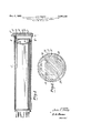
- FIG. 1 is a side view partly in section of a vidicon type tube embodying the invention.
- FIG. 2 is a section taken through the target along the line 2 2 of FIG. 1 and shows the reticles and the dark current reference area incorporated in the target.
- the vidicon tube shown in FIG. 1 is conventional except for the target 1f).
- the tube comprises an elongated glass envelope 12 closed at one end thereof by a transparent faceplate 14 that may be made of glass for example.
- the faceplate 14 is sealed across the end referred to, by means of an indium ring 15 and clamping ring 17.
- the target 1() is positioned on the inner face of the faceplate 14.
- a mesh screen 16 mounted across one end of a tubular focusing electrode 18.
- an electron gun (not shown) for providing an electron beam.
- the electron beam is scanned across the target 10 by suitable means such as electromagnetic coils (not shown) disposed outside of the tubular envelope l2.
- the target 10 is a multilayer structure. It includes a relatively thin layer or film 2li (FIG. 1) of a conducting material such as tin oxide in Contact with the faceplate 14. This layer of tin oxide is transparent and electrically conductive and serves as a signal electrode. Over the conductive layer Ztl are disposed several isolated layers of bismuth. One of these isolated layers of bismuth consists of a layer 22 serving as a dark current reference area. Others of the isolated layers of bismuth consists of four reticles 24, 26, 28 and 30. The reticles serve to define a selected signal area on the target. Over the isolated layers of bismuth and over the exposed layer of tin oxide, is a layer 32 of photoconductive material. The photoconductive material may be a solid layer of a mixture of 67% antimony trisultide and 33% antimony oxysulde, by weight.
- the area of the target scanned by the electron beam is indicated as the rectangle enclosed by the dashed lines 33 in FIG. 2. This area includes the reticles 24, 26, 28, 30 and the dark current reference area 22.
- the thickness of each of the several layers referred to is as follows.
- the tin oxide layer 20 should be thin enough to be light transparent and yet suiciently thick so as to have suflicient lateral conductivity for service as a signal electrode.
- a satisfactory thickness of the tin oxide layer for the purposes of the invention is about one micron.
- the thickness of the photoconductive layer should be about three microns for good results.
- the isolated layers (22 to 23) of bismuth should have a suflicient thickness for rendering the layers opaque to light. The minimum thickness for this purpose is 0.5 micron. Any appreciable increase in the thickness of the bismuth layer beyond 0.5 micron is objectionable for several reasons. Such appreciable increase would render the total thickness of the several target layers on the substrate excessive for good adherence on the substrate.
- each of the signal electrode layer and photoconductive layer is substantially uniform in thickness throughout the area of the target, and an appreciable thick bismuth layer would result in a pronounced step at the edge of the bismuth layer.
- the total thickness of the several layers of the target would be kept below ve microns and preferably at a value of about four and one-half microns to avoid objectionable target peeling.
- the tin oxide layer 20 and the photoconductive layer 32 may be applied by conventional evaporation techniques.
- the isolated bismuth layers are applied as follows.
- the faceplate 14 with its initially applied layer 20 of tin oxide is appropriately masked to expose isolated areas to be covered by bismuth.
- the masking may be effected by holding a clean metal disk against the faceplate, with suitable portions of the disk removed as by etching, to expose only the portions of the faceplate to be coated with bismuth.
- the masked faceplate is suitably supported in a standard bell jar evacuated to a pressure of approximately 1 l0n millimeters of mercury. Also placed in the bell jar is a tantalum boat filled with either bismuth or bismuth oxide. The boat is slidably positioned, e.g., opposite to the masked faceplate, to direct evaporated bismuth upon the masked surface of the faceplate.
- the boat was spaced 9 inches from the faceplate.
- bismuth When bismuth is used in the boat it responds in suitable evaporation when the boat is raised to a temperature of about 250 C. in the vacuum ambient referred to.
- a higher temperature is used, i.e., 900 C. At this temperature the bismuth oxide is reduced to bismuth before it reaches the masked faceplate.
- the evolved oxygen is pumped out of the bell jar.
- the fact that the bismuth or bismuth oxide is in the course of evaporation directed to the masked faceplate precludes major loss by the pumping action.
- the thickness of the bismuth layer deposited on the masked faceplate may be determined optically by means of a monitoring plate.
- the bismuth layers are over and in contact with the tin oxide layer. This will dispose the bismuth layers between the tin oxide and photoconductor layers. This disposition of the bismuth layers is important because the bismuth layers adhere well to the tin oxide layer, and poorly to either the faceplate substrate or to the photoconductor. Another reason for placing the bismuth layers on the tin oxide layer is that the tin oxide layer is applied at a temperature close to 600 C., which It would Il is appreciably above the melting temperature of bismuth which is 271 C.
- bismuth provides a highly effective light shielding medium so that any current owing through areas of the photoconductor shielded by the bismuth, provides an accurate indication of the conductivity of the photoconductor in the dark.
- Bismuth is also electrically conductive so that in combination with the signal plate, it is adapted to provide a true dark current signal.
- the opacity and conductivity of bismuth persist at substantially the same values over widely different temperature conditions of operation. Another and important advantage as pointed out before, is that bismuth adheres well to the tin oxide coating when applied thereon as a layer having suicient thickness to provide opacity.
- the reticles described in the foregoing provide during operation signal areas easily distinguished by the signals derived therefrom from signals derived from any observable scene.
- a better indication of the dark current level is provided by the larger area 22.
- the appreciably larger area 22 (FIG. 2) exposed to the scanning beam provides an easily measurable indication of such level.
- the dark current level indication may be used to automatically adjust signal plate and cathode voltages so that at all times during operation of the tube, the dark current level is below the signal level.
- a composite target structure for a photoconductive pickup tube comprising:
- a photoconductive pickup tube having a target including means defining a signal area, and means dening a dark reference area spaced from said signal area, said last named means comprising:
- said bismuth layer having a thickness of about 0.5
- a photoconductive pickup tube comprising: and are readily distinguishable from the datum area (a) an elongated envelope, of said target. (b) a target in one end portion of said envelope, and 10 7.
- a target for a pickup tube having a signal portion (c) an electron gun in the other end portion of said envelope for providing a beam of electrons adapted to be scanned over a predetermined region of said target during operation of said tube, said predetermined region comprising:
- a target for a photoconductive pickup tube having and a nonsignal portion comprising:
- said layer of bismuth being suiciently thin to preserve a substantially uniform thickness of said signal portion and non-signal portion of said target.
- each of said reticled areas being defined by a structure comprising:
Landscapes
- Engineering & Computer Science (AREA)
- Manufacturing & Machinery (AREA)
- Physics & Mathematics (AREA)
- Electromagnetism (AREA)
- Image-Pickup Tubes, Image-Amplification Tubes, And Storage Tubes (AREA)
Description
Dec. 6, 1966 J. F. HEAGY 3,290,530
PHOTOCONDUCTIVE PICKUP TUBE TARGET WITH @PAGUE SECTION FOR MEASURING DARK CURRENT Filed March ll, 1964 I NVE NTOR.
United States Patent O 3,290,530 PHOTOCONDUCTIVE PICKUP TUBE TARGET WITH OPAQUE SECTION FOR MEASURING DARK CURRENT John F. Heagy, Lancaster, Pa., assignor to Radio Corporation of America, a corporation of Delaware Filed Mar. 11, 1964, Ser. No. 351,148 7 Claims. (Cl. 313-65) The present invention relates to pickup tubes of the photoconductive type, and particularly to a target for such a tube.
A photoconductive pickup tube such as a vidicon normally includes an evacuated elongated envelope having an electron gun in one end thereof adapted to produce a beam of electrons. In the other end portion of the envelope is disposed a target comprising an insulating substrate, a transparent conducting signal plate on the substrate, and a layer of photoconductive material on the signal plate. The beam is caused to scan the target by suitable means such as a system of coordinate electromagnetic deflecting coils positioned outside of the tube envelope.
During operation of a vidicon tube the signal plate is impressed with a positive voltage, which may 'be 30 volts, for example. When an image is focused upon the photoconductive layer, the lighter portions of the image render elemental areas of the photoconductive layer conductive. However it is found that the photoconductive layer is characterized by some conductivity even in the absence of light thereon. This conductivity is relatively low and is known as the dark current level of the photoconductor.
Although the dark current level of the photoconductor is relatively low, it must be taken into account for proper operation of a vidicon. Thus, where the dark current level at a given temperature of operation is known, the voltages on the signal electrode and on the cathode are adjusted to produce a signal level that is at all times above the dark current level. Such adjustment is feasible due to the fact that a change in the voltage difference between the signal plate and the cathode has an appreciably greatter effect on the dark current level than on the signal level. However, when a vidicon is operated in an ambient characterized by appreciable temperature fluctuation, the dark current level also fluctuates. Such fluctuations occur as a consequence of changes in conductivity of the photoconductive layer in response to temperature changes. Thus, the conductivity increases with increase in temperature and decreases with decreasing temperature. Therefore the fluctuations in the dark current level occur upwardly in response to increase in temperature, and downwardly in response to low temperatures. The upward fiuctuations of the dark current level are particularly troublesome. Thus, as such upward fluctuations encroach upon the signal level it may become impossible to distinguish a signal from a non-signal area on the target. In this way, a significant portion of the signal may` be lost.
One prior attempt to determine the dark current level during operation of a tube has involved periodic capping of the lens system with which the tube is used. However,
the periodic capping technique provides time intervals between the capping periods during which the dark current level is not known. The dark current level may rise to objectionable levels during such intervals and result in undetectable interference with the signal output of the tube. Furthermore, the time required for capping may adversely affect the continuity of the signal.
In some types of vidicon tubes it is desirable to provide on the target thereof, reference means in the form of reticles. One ofthe purposes of the reticles is to define 329053011 Patented Dec. 6, 1966 a particular signal area on the target. To perform this purpose properly it is desirable that the reticles be distinguishable from the signal area during tube operation.
Accordingly, it is an object of the invention to provide a photoconductive type of pickup tube in which the dark current level can be accurately and constantly monitored during tube operations.
It is a further object of the invention to provide a dark current reference area on the target of a photoconductive type of pickup tube It is a further object to provide on the target of a photoconductive type pickup tube, indicating means in the form of reticles to define a particular signal area on the target.
Another object is to provide means for determining the dark current level of the photoconductor of a vidicon type tube without adverse effects on the output signal.
A further object is to provide a vidicon tube having on the target thereof a dark current level reference area at a location on the target that is exposed to a scanning beam but displaced from the effective signal area of the target.
A still further object of the invention is to provide a dark current reference area on the target of a vidicon type tube that is effective to provide a true indication of the dark current level under all conditions of tube operation, including operation in ambients of widely different temperatures.
In accordance with the invention, the target for a vidicon, for example, is provided with one or more areas which permit only the flow of dark current during tube operation. Each of such areas on the target comprises a multilayer portion of the target including a layer of conducting material such as tin oxide serving as a signal plate, a layer of bismuth on the layer of tin oxide, and a layer of photoconductive material on the layer of bismuth. One of the multilayer dark current flow areas is effective to provide desirable indications under widely different temperature conditions of operation. Other dark current flow areas may be provided to serve as reticles, if desired.
In the drawing:
FIG. 1 is a side view partly in section of a vidicon type tube embodying the invention, and
FIG. 2 is a section taken through the target along the line 2 2 of FIG. 1 and shows the reticles and the dark current reference area incorporated in the target.
The vidicon tube shown in FIG. 1 is conventional except for the target 1f). The tube comprises an elongated glass envelope 12 closed at one end thereof by a transparent faceplate 14 that may be made of glass for example. The faceplate 14 is sealed across the end referred to, by means of an indium ring 15 and clamping ring 17. The target 1() is positioned on the inner face of the faceplate 14. Closely spaced from the target 10 is a mesh screen 16 mounted across one end of a tubular focusing electrode 18. In the other end portion of the envelope 12 is positioned an electron gun (not shown) for providing an electron beam. The electron beam is scanned across the target 10 by suitable means such as electromagnetic coils (not shown) disposed outside of the tubular envelope l2.
The target 10 is a multilayer structure. It includes a relatively thin layer or film 2li (FIG. 1) of a conducting material such as tin oxide in Contact with the faceplate 14. This layer of tin oxide is transparent and electrically conductive and serves as a signal electrode. Over the conductive layer Ztl are disposed several isolated layers of bismuth. One of these isolated layers of bismuth consists of a layer 22 serving as a dark current reference area. Others of the isolated layers of bismuth consists of four reticles 24, 26, 28 and 30. The reticles serve to define a selected signal area on the target. Over the isolated layers of bismuth and over the exposed layer of tin oxide, is a layer 32 of photoconductive material. The photoconductive material may be a solid layer of a mixture of 67% antimony trisultide and 33% antimony oxysulde, by weight.
The area of the target scanned by the electron beam is indicated as the rectangle enclosed by the dashed lines 33 in FIG. 2. This area includes the reticles 24, 26, 28, 30 and the dark current reference area 22.
The thickness of each of the several layers referred to is as follows. The tin oxide layer 20 should be thin enough to be light transparent and yet suiciently thick so as to have suflicient lateral conductivity for service as a signal electrode. A satisfactory thickness of the tin oxide layer for the purposes of the invention is about one micron. The thickness of the photoconductive layer should be about three microns for good results. The isolated layers (22 to 23) of bismuth should have a suflicient thickness for rendering the layers opaque to light. The minimum thickness for this purpose is 0.5 micron. Any appreciable increase in the thickness of the bismuth layer beyond 0.5 micron is objectionable for several reasons. Such appreciable increase would render the total thickness of the several target layers on the substrate excessive for good adherence on the substrate. also introduce objectionable nonuniformity in the overall thickness of the several target layers. This is because each of the signal electrode layer and photoconductive layer is substantially uniform in thickness throughout the area of the target, and an appreciable thick bismuth layer would result in a pronounced step at the edge of the bismuth layer. The total thickness of the several layers of the target would be kept below ve microns and preferably at a value of about four and one-half microns to avoid objectionable target peeling.
The tin oxide layer 20 and the photoconductive layer 32 may be applied by conventional evaporation techniques. The isolated bismuth layers are applied as follows.
The faceplate 14 with its initially applied layer 20 of tin oxide is appropriately masked to expose isolated areas to be covered by bismuth. The masking may be effected by holding a clean metal disk against the faceplate, with suitable portions of the disk removed as by etching, to expose only the portions of the faceplate to be coated with bismuth. The masked faceplate is suitably supported in a standard bell jar evacuated to a pressure of approximately 1 l0n millimeters of mercury. Also placed in the bell jar is a tantalum boat filled with either bismuth or bismuth oxide. The boat is slidably positioned, e.g., opposite to the masked faceplate, to direct evaporated bismuth upon the masked surface of the faceplate. In one example the boat was spaced 9 inches from the faceplate. When bismuth is used in the boat it responds in suitable evaporation when the boat is raised to a temperature of about 250 C. in the vacuum ambient referred to. When bismuth oxide is employed in the boat, a higher temperature is used, i.e., 900 C. At this temperature the bismuth oxide is reduced to bismuth before it reaches the masked faceplate. The evolved oxygen is pumped out of the bell jar. The fact that the bismuth or bismuth oxide is in the course of evaporation directed to the masked faceplate precludes major loss by the pumping action. The thickness of the bismuth layer deposited on the masked faceplate may be determined optically by means of a monitoring plate.
It is important that the bismuth layers are over and in contact with the tin oxide layer. This will dispose the bismuth layers between the tin oxide and photoconductor layers. This disposition of the bismuth layers is important because the bismuth layers adhere well to the tin oxide layer, and poorly to either the faceplate substrate or to the photoconductor. Another reason for placing the bismuth layers on the tin oxide layer is that the tin oxide layer is applied at a temperature close to 600 C., which It would Il is appreciably above the melting temperature of bismuth which is 271 C.
The use of bismuth to provide a dark current reference area and reticles is of advantage in several respects. Bismuth provides a highly effective light shielding medium so that any current owing through areas of the photoconductor shielded by the bismuth, provides an accurate indication of the conductivity of the photoconductor in the dark. Bismuth is also electrically conductive so that in combination with the signal plate, it is adapted to provide a true dark current signal. Furthermore, the opacity and conductivity of bismuth persist at substantially the same values over widely different temperature conditions of operation. Another and important advantage as pointed out before, is that bismuth adheres well to the tin oxide coating when applied thereon as a layer having suicient thickness to provide opacity.
The reticles described in the foregoing provide during operation signal areas easily distinguished by the signals derived therefrom from signals derived from any observable scene. A better indication of the dark current level is provided by the larger area 22. The appreciably larger area 22 (FIG. 2) exposed to the scanning beam provides an easily measurable indication of such level. If desired, the dark current level indication may be used to automatically adjust signal plate and cathode voltages so that at all times during operation of the tube, the dark current level is below the signal level.
What is claimed is:
1. A photoconductive pickup tube having a target, said target comprising:
(a) an insulating substrate,
(b) a conductive layer on said substrate,
(c) an opaque layer of bismuth on only a portion of said conductive layer, whereby another portion of said conductive layer is exposed, and
(d) a layer of photoconductive material on said exposed portion of said conductive layer and on said bismuth layer.
2. A photoconductive pickup tube having a target, said target comprising:
(a) an insulating substrate,
(b) a light transparent conductive layer on said substrate,
(c) an opaque layer of bismuth covering only a portion of said conductive layer,
(d) said layer of bismuth being thinner than said conductive layer, and
(e) a continuous layer of photoconductive material on both said layer of bismuth and on the portion of said conductive layer not covered by said layer of bismuth.
3. A composite target structure for a photoconductive pickup tube comprising:
(a) a flat insulating substrate having a target area,
(b) a plurality of material layers on said target area of said substrate having a total thickness of about 4.5 microns, said layers comprising:
(1) a layer of conductive material on said substrate and substantially coextensive with said target area,
(2) a layer of photoconductive material substantially coextensive with said layer of conductive material, and
(3) a layer of bismuth between said conductive and photoconductive layers, said layer of bismuth extending over only a portion of said target area and having a thickness only sufficient to render said layer of bismuth opaque to light.
4. A photoconductive pickup tube having a target including means defining a signal area, and means dening a dark reference area spaced from said signal area, said last named means comprising:
(a) an insulating substrate,
(b) a conductive layer on said substrate,
(c) a bismuth layer on said conductive layer, and
(d) a photoconductive layer on said bismuth layer,
(e) said bismuth layer having sufficient thickness to render it opaque to light,
(f) whereby current flow through said photoconductive (b) a conducting layer on said substrate,
(c) a bismuth layer on said conducting layer, and
(d) a photoconductive layer on said bismuth layer,
(e) said bismuth layer having a thickness of about 0.5
micron for rendering said layer opaque to light,
layer to said bismuth layer constitutes the dark cur- 5 (f) whereby said reticled areas are characterized only rent level of said photoconductive layer. by dark current flow during operation of said tube 5. A photoconductive pickup tube comprising: and are readily distinguishable from the datum area (a) an elongated envelope, of said target. (b) a target in one end portion of said envelope, and 10 7. A target for a pickup tube having a signal portion (c) an electron gun in the other end portion of said envelope for providing a beam of electrons adapted to be scanned over a predetermined region of said target during operation of said tube, said predetermined region comprising:
(l) a signal plate,
(2) a photoconductive layer over said signal plate,
and
(3) a bismuth layer between said signal plate and photoconductive layer and extending across a portion only of the interface area between said signal plate and photoconductive layer at said predetermined region, said bismuth layer having a thickness suicient to render it opaque to light,
(4) whereby current flowing through the portion of said photoconductor over said bismuth layer, during operation of said tube, constitutes the dark current level of said photoconductive layer.
6. A target for a photoconductive pickup tube having and a nonsignal portion, said target comprising:
(a) a conducting layer on said signal portion and nonsignal portion,
(b) a layer of bismuth only on said non-signal portion of said conducting layer, and
(c) a layer of photoconductive material on said layer of bismuth in said non-signal portion and on said conducting layer in said signal portion,
(d) said bismuth layer having a thickness for rendering it substantially opaque to light,
(e) said layers of bismuth and photoconductive material having a combined thickness of less than five microns for good adherence of said bismuth and photoconductive layers on said conducting layer,
(f) said layer of bismuth being suiciently thin to preserve a substantially uniform thickness of said signal portion and non-signal portion of said target.
No references cited.
thereon a plurality of reticled areas in predetermined space relation to a datum area of said target, each of said reticled areas being defined by a structure comprising:
(a) an insulating substrate,
JAMES W. LAWRENCE, Primary Examiner.
R. SEGAL, Assistant Examiner.
Claims (1)
1. A PHOTOCONDUCTIVE PICKUP TUBE HAVING A TARGET, SAID TARGET COMPRISING: (A) AN INSULATING SUBSTRATE, (B) A CONDUCTIVE LAYER ON SAID SUBSTRATE, (C) AN OPAQUE LAYER OF BISMUTH ON ONLY A PORTION OF SAID CONDUCTIVE LAYER, WHEREBY ANOTHER PORTION OF SAID CONDUCTIVE LAYER IS EXPOSED, AND (D) A LAYER OF PHOTOCONDUCTIVE MATERIAL ON SAID EXPOSED PORTION OF SAID CONDUCTIVE LAYER AND ON SAID BISMUTH LAYER.
Priority Applications (1)
| Application Number | Priority Date | Filing Date | Title |
|---|---|---|---|
| US351148A US3290530A (en) | 1964-03-11 | 1964-03-11 | Photoconductive pickup tube target with opaque section for measuring dark current |
Applications Claiming Priority (1)
| Application Number | Priority Date | Filing Date | Title |
|---|---|---|---|
| US351148A US3290530A (en) | 1964-03-11 | 1964-03-11 | Photoconductive pickup tube target with opaque section for measuring dark current |
Publications (1)
| Publication Number | Publication Date |
|---|---|
| US3290530A true US3290530A (en) | 1966-12-06 |
Family
ID=23379768
Family Applications (1)
| Application Number | Title | Priority Date | Filing Date |
|---|---|---|---|
| US351148A Expired - Lifetime US3290530A (en) | 1964-03-11 | 1964-03-11 | Photoconductive pickup tube target with opaque section for measuring dark current |
Country Status (1)
| Country | Link |
|---|---|
| US (1) | US3290530A (en) |
Cited By (4)
| Publication number | Priority date | Publication date | Assignee | Title |
|---|---|---|---|---|
| US3418508A (en) * | 1967-08-23 | 1968-12-24 | Gen Electrodynamics Corp | Photoconductive layer separated from reactive opaque pattern by transparent conductive layer |
| US3505551A (en) * | 1966-10-24 | 1970-04-07 | Gen Electrodynamics Corp | Photoconductive layer having reduced resistivity portions in pattern form |
| US3519866A (en) * | 1967-09-26 | 1970-07-07 | Rca Corp | Photoconductive pickup tube having opaque gold pattern encapsulated in tin oxide layer |
| US3927340A (en) * | 1973-02-09 | 1975-12-16 | Hitachi Ltd | Imaging target for photoconduction type image pickup device |
-
1964
- 1964-03-11 US US351148A patent/US3290530A/en not_active Expired - Lifetime
Non-Patent Citations (1)
| Title |
|---|
| None * |
Cited By (4)
| Publication number | Priority date | Publication date | Assignee | Title |
|---|---|---|---|---|
| US3505551A (en) * | 1966-10-24 | 1970-04-07 | Gen Electrodynamics Corp | Photoconductive layer having reduced resistivity portions in pattern form |
| US3418508A (en) * | 1967-08-23 | 1968-12-24 | Gen Electrodynamics Corp | Photoconductive layer separated from reactive opaque pattern by transparent conductive layer |
| US3519866A (en) * | 1967-09-26 | 1970-07-07 | Rca Corp | Photoconductive pickup tube having opaque gold pattern encapsulated in tin oxide layer |
| US3927340A (en) * | 1973-02-09 | 1975-12-16 | Hitachi Ltd | Imaging target for photoconduction type image pickup device |
Similar Documents
| Publication | Publication Date | Title |
|---|---|---|
| US3350595A (en) | Low dark current photoconductive device | |
| US3293474A (en) | Phosphor dielectric storage target for cathode ray tube | |
| US2177736A (en) | Television transmitting apparatus | |
| US2169840A (en) | Cathode-ray signal-generating tube | |
| US2622219A (en) | Television image tube | |
| US3290530A (en) | Photoconductive pickup tube target with opaque section for measuring dark current | |
| US3405298A (en) | Photoconductive device having a target including a selenium blocking layer | |
| US3046431A (en) | Storage system | |
| US3391022A (en) | Photoconductive layer and method of making the same | |
| US2881340A (en) | Photoconductive television pickup tube | |
| US2212923A (en) | Picture transmitter | |
| US3020442A (en) | Photoconductive target | |
| US3271608A (en) | X-ray vidicon target assembly | |
| US2970219A (en) | Use of thin film field emitters in luminographs and image intensifiers | |
| US2175691A (en) | Photovoltaic target | |
| US3148297A (en) | Electron device with storage capabilities | |
| US3268764A (en) | Radiation sensitive device | |
| US3370168A (en) | Anode aperture plate for a television camera tube in an electron microscope comprising a stainless steel foil | |
| GB977428A (en) | Image tubes | |
| US2289921A (en) | Photosensitive electrode | |
| US2198327A (en) | Mosaic electrode structure | |
| US3315108A (en) | High lag, high sensitivity target having solid antimony oxysulphide and porous antimony trisulphide layers | |
| US3020432A (en) | Photoconductive device | |
| US3519866A (en) | Photoconductive pickup tube having opaque gold pattern encapsulated in tin oxide layer | |
| US2843774A (en) | Light absorbent surfaces |