US3239694A - Bi-level threshold setting circuit - Google Patents
Bi-level threshold setting circuit Download PDFInfo
- Publication number
- US3239694A US3239694A US311462A US31146263A US3239694A US 3239694 A US3239694 A US 3239694A US 311462 A US311462 A US 311462A US 31146263 A US31146263 A US 31146263A US 3239694 A US3239694 A US 3239694A
- Authority
- US
- United States
- Prior art keywords
- voltage
- level
- transistor
- reference voltage
- comparator
- Prior art date
- Legal status (The legal status is an assumption and is not a legal conclusion. Google has not performed a legal analysis and makes no representation as to the accuracy of the status listed.)
- Expired - Lifetime
Links
- 238000010586 diagram Methods 0.000 description 7
- 230000008859 change Effects 0.000 description 6
- 238000005513 bias potential Methods 0.000 description 3
- 230000008878 coupling Effects 0.000 description 3
- 238000010168 coupling process Methods 0.000 description 3
- 238000005859 coupling reaction Methods 0.000 description 3
- 230000004044 response Effects 0.000 description 3
- 230000009471 action Effects 0.000 description 2
- 238000012986 modification Methods 0.000 description 2
- 230000004048 modification Effects 0.000 description 2
- 239000003990 capacitor Substances 0.000 description 1
- 230000000295 complement effect Effects 0.000 description 1
- 230000000694 effects Effects 0.000 description 1
- 230000001172 regenerating effect Effects 0.000 description 1
Images


Classifications
-
- H—ELECTRICITY
- H03—ELECTRONIC CIRCUITRY
- H03K—PULSE TECHNIQUE
- H03K3/00—Circuits for generating electric pulses; Monostable, bistable or multistable circuits
- H03K3/02—Generators characterised by the type of circuit or by the means used for producing pulses
- H03K3/26—Generators characterised by the type of circuit or by the means used for producing pulses by the use, as active elements, of bipolar transistors with internal or external positive feedback
- H03K3/28—Generators characterised by the type of circuit or by the means used for producing pulses by the use, as active elements, of bipolar transistors with internal or external positive feedback using means other than a transformer for feedback
- H03K3/281—Generators characterised by the type of circuit or by the means used for producing pulses by the use, as active elements, of bipolar transistors with internal or external positive feedback using means other than a transformer for feedback using at least two transistors so coupled that the input of one is derived from the output of another, e.g. multivibrator
- H03K3/286—Generators characterised by the type of circuit or by the means used for producing pulses by the use, as active elements, of bipolar transistors with internal or external positive feedback using means other than a transformer for feedback using at least two transistors so coupled that the input of one is derived from the output of another, e.g. multivibrator bistable
- H03K3/2893—Bistables with hysteresis, e.g. Schmitt trigger
- H03K3/2897—Bistables with hysteresis, e.g. Schmitt trigger with an input circuit of differential configuration
Definitions
- This invention relates to a voltage level detector or threshold setting circuit, and more particularly to a threshold setting circuit which is alternately set to independent threshold levels in response to the signal being compared as it passes through the threshold levels in alternating directions.
- a threshold setting circuit is often required in electronic systems, usually so that only that part of a signal above a certain noise level is transmitted to a load.
- An example is the read channel of a magnetic drum or disc memory of a data processing system, particularly if nonreturn-to-zero (NRZ) recording has been employed.
- Noise threshold setting is particularly necessary in the playback or read channel of an NRZ recorded memory system because a pulse occurs only when there is a change in value of successively recorded binary digits, i.e., only when a binary digit 1 or O is followed by a binary digit or 1, respectively. At other times there is no read sig-.
- the threshold setting necessary with NRZ recording should be bi-level or bipolar because the polarity of the signal read reverses each time there is a change in the value of successively recorded binary digits.
- Bipolar threshold circuits have been devised in the past; however, such circuits have not always been satisfactory. For instance, they have not been adjustable such that the threshold level of each polarity may be set independently.
- Another shortcoming of the prior art circuits is that the output signal is present only when the input signal is above the threshold level, which imposes narrow limita tions on strobe timing in the reading channel.
- a threshold setting circuit is provided which is set to a second threshold level when the input signal passes through a first threshold level in one direction and is reset to its first threshold level only when the input signal passes through the second threshold level in the opposite direction.
- an object of this invention is to provide A further object is to provide a bi-level threshold setting circuit in which threshold levels are established by independent reference voltages, each established by a single voltage source.
- a voltage comparator having two input terminals and an output terminal.
- a reference voltage of one polarity is coupled to one input terminal of the comparator for comparison with a signal coupled to the other input terminal.
- an output signal actuates a means for switching an independent reference voltage of the opposite polarity to the first input terminal. In that manner the comparator is not reset when the input to provide an output signal of a given amplitude until the input signal exceeds the second reference voltage in the opposite sense or polarity.
- FIG. 1 is a circuit diagram of a first embodiment of the invention
- FIG. 2 is a schematic block diagram of a read channel in a magnetic drum or di-sc memory in which the present invention may be employed;
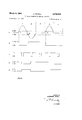
- FIG. 3 isa timing diagram of wave forms appearing at indicated points of the block diagram in FIG. 2;
- FIG. 4 is a schematic diagram of a second embodiment of the invention.
- a differential amplifier comprising NPN transistors Q and Q is provided for comparing input voltage e across input terminals 10 and 11 with a reference voltage e appearing across a resistor 12 connected between the base of transistor Q and ground.
- a resistor 13 and a diode D are connected in series between a voltage source V and the resistor 12 to provide a negative reference voltage at the base of the transistor Q
- the diode D is connected with its cathode to the resistor 13 and its anode connected to the resistor 12 so that the voltage dividing network providing a negative reference voltage at the base of the transistor Q effectively consists of only the resistor 12 and the resistor 13.
- transistor Q is conducting and the transistor Q is cut off.
- a third transistor Q is also cut otf because it is of the PNP type and has its base connected to the collector of the transistor Q which is connected by a resistor 14 to a voltage source of +V and has its emitter connected to a less positive voltage source +V
- a diode D connected between the base and emitter electrodes of the transistor Q protects the base-to-emitter junction by preventing the base electrode from being biased more positive with respect to the emitter or +V than the voltage drop across it.
- the circuit will remain in that state with only transistor Q conducting until the input signal e becomes more negative than the reference voltage e;,, at which time the transistor Q is turned off and the transistor Q turned on owing to a common emitter resistor 16.
- a negative output signal at the collector of the transistor Q is inverted by the transistor Q and fed back to the base of the transistor Q through a resistor 15, making the reference voltage e less negative.
- This feedback signal causes a regenerative action to ensue until the transistor Q is cut oif owing to a common emitter resistor 16 and the transistor Q is driven to saturation.
- the reference voltage e at the base of the transistor Q is determined by the following equation:
- V is the saturation voltage of the transistor Q
- R is the resistance of resistor 12
- R is the resistance of resistor 15. If the voltage +V applied to the emitter of the transistor Q is chosen to be much larger than V the tolerance on the reference voltage +e applied to the base of the transistor Q is determined primarily by the tolerance on the voltage supply +V and the tolerance on the voltage dividing network comprising the resistors 12 and 15.
- the overall tolerance on the operation of the threshold setting circuit is affected by the tolerance achieved on the positive and negative reference voltages, and by the characteristics of the transistors and diodes employed. Any difference in the base-to-ernitter voltages V of the transistors Q and Q will be added or subtracted from the threshold setting level. Another factor which aifects overall tolerance is changes in the DC. current gain of the transistor Q All of the effects caused by the transistor characteristics may be eliminated by properly adjusting the resistors 13 and 15.
- the positive reference voltage may be adjusted by changing the value of the resistor 15.
- the negative voltage reference may be adjusted by varying the value of the resistor 13. If it is desired to maintain the negative reference voltage equal in magnitude to the positive reference voltage, both may be adjusted in magnitude equally by varying only the value of the resistor 12.
- the reference voltages thus separately established and adjusted are further independent in that each depends upon a separate power supply,
- FIG. 2 discloses a playback or readout channel of an NRZ recorded memory system in which a pulse occurs only when there is a change in value of successively recorded binary digits.
- a read-head 21 senses the recorded digits, such as 10011 for the illustrated waveform of FIG. 3, as a track on a magnetic disc or drum 22 is rotated.
- An amplifier 23 couples the read-head 21 to the input of a threshold setting circuit 24. If it is required that the theshold setting circuit detect magnitudes of a signal having a quiescent level which is not ground, or which may vary from ground potential, A.C. coupling may be employed, such as a capacitor 25 and inductor 26 as shown.
- the threshold setting circuit of FIG. 1 may be advantageously used as the threshold setting circuit 24 in the read channel of FIG. 2. In a typical application it accepts read signals which have been amplified to a peak value exceeding .75 volt, and rejects noise signals of a peak value not exceeding .50 volt if the reference voltages are -.62 volts.
- the output represented by the waveform B of FIG. 3 remains at a high level until the input waveform A exceeds the threshold level of +.62 v. at time T whereupon the threshold circuit is reset as described hereinbefore with reference to FIG. 1 to provide a -.62 v. reference. Accordingly, the output waveform B remains at a lower level until the waveform A exceeds --.62 v. in the mega tive direction at time T whereupon the threshold setting circuit is again set to provide a +.62 v. reference.
- the voltage level of the waveform B is changed from the lower level to the upper level only when the recorded digits being sensed change from a binary 1 to a binary -0.
- the upper level of the waveform B then represents a binary 0 and the lower level represents a binary 1.
- the next two digits to be sensed are 0 and 1.
- a pulse does not occur since it is the same as the preceding digit read; but when the digit 1 is sensed, a pulse occurs which exceeds the 62 v. reference and resets the threshold setting circuit 24 to provide a lower level output signal and a -.62 v. reference. Since the last digit is a l, a pulse does not occur during the last period and the waveform B remains at a lower level, indicating that a binary digit 1 is sensed during the last period.
- a strobe pulse source 27 transmits a negative 0 to 6 v. pulse through a strobe switch 28 to set or reset a flipflop 29 according to whether a binary digit 1 or binary digit 0 is being sensed during successive periods.
- the waveforms C, D and E of FIG. 3 indicate the signals present on the corresponding lines C, D and E of FIG. 2 to accomplish that.
- FIG. 4 is a circuit diagram of a second embodiment of the invention and a circuit diagram for the strobe switch 28.
- the threshold setting circuit comprises transistors Q Q and Q which are arranged in a manner similar to the cicuit of FIG. 1.
- the transistor Q is of the NPN type whereas the corresponding transistor Q of FIG. 1 is of the PNP type. Accordingly, the operation of the threshold setting circuit in FIG. 4 differs in that while the transistor Q is conducting the transistor Q is cut off and while the tran sistor Q is cut oif the transistor Q is conducting at saturation.
- the transistor Q is cut oif, the transistor Q is conducting and the transistor Q is cut off.
- .62 v. is then established by the voltage dividing network consisting of resistor 32, diode D and resistor 33 connected in series between a source of +12 v. and ground.
- the transistor Q is turned on and the transistor Q is turned off.
- the transistor Q cut off, its collector electrode potential increases toward +12 v.
- a Zener diode D provides a drop of 9 volts to the base of the transistor Q so that a +3 v. signal drives the transistor Q into saturation.
- the transistor Q With the transistor Q conducting at saturation, its collector electrode drops from about 1.5 volts to about 5 volts whereupon the diode D is reverse-biased and a reference voltage of -.'62 v. is provided at the base of the transistor Q by the voltage dividing network comprising resistors 32 and 35 connected in series.
- a switch 36 is momentarily closed to establish a reference voltage of l.-62 v. by the voltage dividing action of a resistor 3-7 and diode B in series with the resistor 32 between a source of +6 v. and ground.
- a resistor 38 connected to a 3 v. source reverse-biases the diode D If the threshold setting circuit is to be initially set with a reference voltage of .62 v. at the base of the transistor Q a switch 41 is momentarily closed instead to provide a reference voltage of .62 v.
- the strobe switch 28 is coupled to the threshold setting circuit by a diode D having its anode connected to the base of a transistor Q which is biased by a resistor 50 connected to a source of 3 v. and a resistor 51 connected to ground.
- the strobe switch comprises the transistor Q and a transistor Q connected to a source of negative-going (0 to 6 v.) strobe pulses from the source 27 by a common emitter resistor 52.
- the strobe switch is essentially a differential amplifier which transmits a current pulse to the flip-flop 29 over a line D or E upon the occurrence of a negative-going strobe pulse depending upon Whether an upper level signal of about +1.3 v. is being transmitted to the diode D or a lower level signal of about 6 v. If an upper level signal is being transmitted by the threshold setting circuit, the negative-going strobe pulse is effectively steered to the line B to reset the flipflop 29, thereby indicating that a binary digit 0 has just been read. Similarly, if a lower level signal is being transmitted, the strobe pulse is elfectively steered to the line D through the transistor Q which has its base connected to a source of 3 v. to set the flip-flop29, therebv indicating that a binary digit 1 has just been read.
- both of the lines D and E are clamped to ground by diodes D and D to prevent the input terminals of the flip-flop 29 from being driven below .7 volt.
- the manner in which the collectors of the transistors Q and Q are to be connected to the fiip-flop 29 depends upon the circuit c'onfiguration of the flip-flop itself.
- the flipflop comprises two cross-coupled NPN transistors Q and Q each biased in a common-emitter configuration. The base electrodes of the transistors Q and Q are directly connected to the collector electrodes of the transistors Q and Q respectively.
- a voltage dividing network comprising resistors 69 and 61 connected between ground (through the conducting transistor Q and the source .of 3 v. holds the collector of the transistor Q at .7 v. while a voltage dividing network comprising resistors 63,
- a threshold setting circuit comprising a voltage comparator having two input terminals and an output terminal, means for applying a reference voltage of a preselected first level and polarity to one of said input terminals, means for applying a voltage signal to the other of said input terminals for comparison With a reference voltage, and means coupled to the output terminal of said comparator for switching said reference voltage to a prese-' lected second level of opposite polarity from said first level when said comparator detects that said voltage signal exceeds said preselected first level in a given sense, and for returning said reference voltage to said preselected first level when said comparator detects that said voltage signal exceeds said preselected second level in an opposite sense.
- a threshold setting circuit comprising a voltage comparator having first and second input terminals and an output terminal
- a threshold setting circuit comprising a voltage comparator having first and second input terminals and an output terminal
- a second voltage dividing network for applying said reference voltage of a preselected second level of opposite polarity from said first level to said second input terminal
- a bipolar threshold setting circuit comprising a voltage comparator having first and second input terminals and an output terminal
- a voltage dividing network coupled at one end to a source of voltage of a first polarity and connected at the other end to ground for applying a reference voltage of a first level and polarity to said second input terminal
- said last mentioned means comprises a low impedance switch responsive to the output of said comparator.
- a unidirectional current conducting device connected in parallel with said first resistor and poled for forward current conduction through said second source of voltage.
- a bipolar threshold setting circuit as defined by claim 6 wherein said comparator comprises first and second transistors
- said switching means comprises a third transistor having its base electrode connected to the collector electrode of said second transistor, its emitter electrode connected to said second source or voltage, and its collector electrode connected to the one end of said voltage dividing network.
- the base electrode of said third transistor is coupled to said source of bias potential of said given polarity by a resistor, and to the collector electrode of said second transistor by a zener diode poled for constant voltage drop between the collector of said second transitsor and the base of said third transistor.
- a bipolar threshold setting circuit as defined by claim 7 including means for momentarily applying to the base of said second transistor a voltage equal to said first reference voltage to set said comparator at a predetermined state of conductivity in the absence of an input signal of the same polarity and equal to or greater than said first reference voltage.
- a read channel comprising a voltage comparator having two input terminals and an output terminal
- a source of strobe pulses connected to said strobe switch for translation to said flip-flop to set or reset said flip-flop according to whether said reference voltage is at said first or second level.
- a read channel comprising a voltage comparator having first and second input terminals and an output terminal
- a voltage dividing network for applying said reference voltage of a first level to said second input terminal
- a source of strobe pulses connected to said strobe switch for translation to said flip-flop to set or reset said flip-flop according to whether said reference voltage is at said first or second level.
- a read channel com prising a voltage comparator having first and second input terminals and an output terminal
- a voltage dividing network coupled at one end to a source of voltage of a first polarity and connected at the other end to ground for applying a reference voltage of a first level and polarity to said second input terminal
- a source or strobe pulses connected to said strobe switch for translation to said flip-flop to set or reset said flip-flop according to whether said reference voltage is at said first or second level and polarity.
Landscapes
- Engineering & Computer Science (AREA)
- Power Engineering (AREA)
- Manipulation Of Pulses (AREA)
Description
March 8, 1966 Filed Sept. 25, 1963 A. ROVELL BI-LEVEL THRESHOLD SETTING CIRCUIT l l @IAMPLIFIER FIG. 2
THRESHOLD SETTING CIRCUIT 5 Sheets-Sheet l FLIP FLOP STROBE SWITCH STROBE PULSE ,"27 SOURCE INVENTOR. ALEXANDER ROVELL ATTORNEY March 8, 1966 A. ROVELL 3,239,694
BI-LEVEL THRESHOLD SETTING CIRCUIT Filed Sept. 25, 1965 3 Sheets-Sheet 2 FIG. 3
INVENTOR. ALEXANDER ROVELL ATTORNEY BI-LEVEL THRESHOLD SETTING CIRCUIT Filed Sept. 25, 1963 3 Sheets-Sheet 5- STROBE PULSE 27 SOURCE FIG 4 IN V EN TOR.
ALEXANDER ROVELL BY%%M AT TORNEY United States Patent Office.
3,239fi94 Patented Mar. 8, 1966 3,239,694 BI-LEVEL THRESHOLD SETTING CIRCUIT Alexander Rovell, Pico Rivera, Califl, assignor to North American Aviation, Inc. Filed Sept. 25, 1963, Ser. No. 311,462 14 Claims. (Cl. 307-885) This invention relates to a voltage level detector or threshold setting circuit, and more particularly to a threshold setting circuit which is alternately set to independent threshold levels in response to the signal being compared as it passes through the threshold levels in alternating directions.
A threshold setting circuit is often required in electronic systems, usually so that only that part of a signal above a certain noise level is transmitted to a load. An example is the read channel of a magnetic drum or disc memory of a data processing system, particularly if nonreturn-to-zero (NRZ) recording has been employed.
Noise threshold setting is particularly necessary in the playback or read channel of an NRZ recorded memory system because a pulse occurs only when there is a change in value of successively recorded binary digits, i.e., only when a binary digit 1 or O is followed by a binary digit or 1, respectively. At other times there is no read sig-.
nal; but there may be noise present which, in the absence of some threshold setting circuit, may be interpreted as a change in value of successively recorded binary digits. If such a mistake is made, all subsequent binary digits read in a group or word are incorrect.
The threshold setting necessary with NRZ recording should be bi-level or bipolar because the polarity of the signal read reverses each time there is a change in the value of successively recorded binary digits. Bipolar threshold circuits have been devised in the past; however, such circuits have not always been satisfactory. For instance, they have not been adjustable such that the threshold level of each polarity may be set independently.
Another shortcoming of the prior art circuits is that the output signal is present only when the input signal is above the threshold level, which imposes narrow limita tions on strobe timing in the reading channel. In an NRZ recording system, such a limitation may be readily alleviated if a threshold setting circuit is provided which is set to a second threshold level when the input signal passes through a first threshold level in one direction and is reset to its first threshold level only when the input signal passes through the second threshold level in the opposite direction.
Accordingly, an object of this invention is to provide A further object is to provide a bi-level threshold setting circuit in which threshold levels are established by independent reference voltages, each established by a single voltage source.
These and other objects of the invention are achieved by providing a voltage comparator having two input terminals and an output terminal. A reference voltage of one polarity is coupled to one input terminal of the comparator for comparison with a signal coupled to the other input terminal. When the signal exceeds the reference voltage in the same sense or polarity, an output signal actuates a means for switching an independent reference voltage of the opposite polarity to the first input terminal. In that manner the comparator is not reset when the input to provide an output signal of a given amplitude until the input signal exceeds the second reference voltage in the opposite sense or polarity.
Other objects and advantages will become apparent from the following description in conjunction with the drawings in which- FIG. 1 is a circuit diagram of a first embodiment of the invention;
FIG. 2 is a schematic block diagram of a read channel in a magnetic drum or di-sc memory in which the present invention may be employed;
FIG. 3 isa timing diagram of wave forms appearing at indicated points of the block diagram in FIG. 2; and
FIG. 4 is a schematic diagram of a second embodiment of the invention.
Referring now to a first embodiment of the invention illustrated in FIG. 1, a differential amplifier comprising NPN transistors Q and Q is provided for comparing input voltage e across input terminals 10 and 11 with a reference voltage e appearing across a resistor 12 connected between the base of transistor Q and ground. A resistor 13 and a diode D are connected in series between a voltage source V and the resistor 12 to provide a negative reference voltage at the base of the transistor Q The diode D is connected with its cathode to the resistor 13 and its anode connected to the resistor 12 so that the voltage dividing network providing a negative reference voltage at the base of the transistor Q effectively consists of only the resistor 12 and the resistor 13.
If the input signal e is 0 volts, and if the reference voltage e is negative, then transistor Q is conducting and the transistor Q is cut off. A third transistor Q is also cut otf because it is of the PNP type and has its base connected to the collector of the transistor Q which is connected by a resistor 14 to a voltage source of +V and has its emitter connected to a less positive voltage source +V A diode D connected between the base and emitter electrodes of the transistor Q protects the base-to-emitter junction by preventing the base electrode from being biased more positive with respect to the emitter or +V than the voltage drop across it.
The circuit will remain in that state with only transistor Q conducting until the input signal e becomes more negative than the reference voltage e;,, at which time the transistor Q is turned off and the transistor Q turned on owing to a common emitter resistor 16.
A negative output signal at the collector of the transistor Q is inverted by the transistor Q and fed back to the base of the transistor Q through a resistor 15, making the reference voltage e less negative. This feedback signal causes a regenerative action to ensue until the transistor Q is cut oif owing to a common emitter resistor 16 and the transistor Q is driven to saturation.
When the circuit is in its second conductive state, the reference voltage e at the base of the transistor Q is determined by the following equation:
where V is the saturation voltage of the transistor Q R is the resistance of resistor 12; and R is the resistance of resistor 15. If the voltage +V applied to the emitter of the transistor Q is chosen to be much larger than V the tolerance on the reference voltage +e applied to the base of the transistor Q is determined primarily by the tolerance on the voltage supply +V and the tolerance on the voltage dividing network comprising the resistors 12 and 15.
It should be noted that when the transistor Q is driven to saturation to couple a positive voltage +V to the junction between the resistors 13 and 15, the diode D is reverse-biased and the voltage at a terminal 20 is at voltage level determined by the following equation:
3+ Dl) R12 2 R12+Rt where V is the voltage drop across the diode D and R is the resistance of resistor 13. If the voltage -V is chosen to be much large than V the tolerance on the reference voltage e is determined primarily by the tolerance on the voltage supply V and the tolerance on the voltage divider comprising resistors 12 and 13. The circuit remains in this first state until the input signal e becomes equal to or more negative than the negative reference voltage e Until then, the voltage at the output terminal remains :at a negative level equal to- 2+ VD1)- An exemplary circuit which operates in accordance with the foregoing description may be provided by using the following values for resistors and. voltage supplies:
'Resistor 12:620 ohms Resistor 13:8.8K ohms Resistor 14=36K ohms Resistor 15:9:1K ohms Resistor 16:9.3K ohms With those values, the amplitude of both the positive and negative reference voltages provided in accordance with the foregoing equations is :62 volt.
The overall tolerance on the operation of the threshold setting circuit is affected by the tolerance achieved on the positive and negative reference voltages, and by the characteristics of the transistors and diodes employed. Any difference in the base-to-ernitter voltages V of the transistors Q and Q will be added or subtracted from the threshold setting level. Another factor which aifects overall tolerance is changes in the DC. current gain of the transistor Q All of the effects caused by the transistor characteristics may be eliminated by properly adjusting the resistors 13 and 15. The positive reference voltage may be adjusted by changing the value of the resistor 15. Similarly, the negative voltage reference may be adjusted by varying the value of the resistor 13. If it is desired to maintain the negative reference voltage equal in magnitude to the positive reference voltage, both may be adjusted in magnitude equally by varying only the value of the resistor 12. The reference voltages thus separately established and adjusted are further independent in that each depends upon a separate power supply,
FIG. 2 discloses a playback or readout channel of an NRZ recorded memory system in which a pulse occurs only when there is a change in value of successively recorded binary digits. A read-head 21 senses the recorded digits, such as 10011 for the illustrated waveform of FIG. 3, as a track on a magnetic disc or drum 22 is rotated. An amplifier 23 couples the read-head 21 to the input of a threshold setting circuit 24. If it is required that the theshold setting circuit detect magnitudes of a signal having a quiescent level which is not ground, or which may vary from ground potential, A.C. coupling may be employed, such as a capacitor 25 and inductor 26 as shown.
The threshold setting circuit of FIG. 1 may be advantageously used as the threshold setting circuit 24 in the read channel of FIG. 2. In a typical application it accepts read signals which have been amplified to a peak value exceeding .75 volt, and rejects noise signals of a peak value not exceeding .50 volt if the reference voltages are -.62 volts.
In operation, assuming the threshold circuit 24 to be initially set with a +.62 v. reference voltage, the output represented by the waveform B of FIG. 3 remains at a high level until the input waveform A exceeds the threshold level of +.62 v. at time T whereupon the threshold circuit is reset as described hereinbefore with reference to FIG. 1 to provide a -.62 v. reference. Accordingly, the output waveform B remains at a lower level until the waveform A exceeds --.62 v. in the mega tive direction at time T whereupon the threshold setting circuit is again set to provide a +.62 v. reference. In that manner, the voltage level of the waveform B is changed from the lower level to the upper level only when the recorded digits being sensed change from a binary 1 to a binary -0. The upper level of the waveform B then represents a binary 0 and the lower level represents a binary 1.
The next two digits to be sensed are 0 and 1. When the digit 0 is sensed, a pulse does not occur since it is the same as the preceding digit read; but when the digit 1 is sensed, a pulse occurs which exceeds the 62 v. reference and resets the threshold setting circuit 24 to provide a lower level output signal and a -.62 v. reference. Since the last digit is a l, a pulse does not occur during the last period and the waveform B remains at a lower level, indicating that a binary digit 1 is sensed during the last period.
A strobe pulse source 27 transmits a negative 0 to 6 v. pulse through a strobe switch 28 to set or reset a flipflop 29 according to whether a binary digit 1 or binary digit 0 is being sensed during successive periods. The waveforms C, D and E of FIG. 3 indicate the signals present on the corresponding lines C, D and E of FIG. 2 to accomplish that.
FIG. 4 is a circuit diagram of a second embodiment of the invention and a circuit diagram for the strobe switch 28. The threshold setting circuit comprises transistors Q Q and Q which are arranged in a manner similar to the cicuit of FIG. 1. However, it should be noted that the transistor Q is of the NPN type whereas the corresponding transistor Q of FIG. 1 is of the PNP type. Accordingly, the operation of the threshold setting circuit in FIG. 4 differs in that while the transistor Q is conducting the transistor Q is cut off and while the tran sistor Q is cut oif the transistor Q is conducting at saturation.
Assuming an initial reference voltage on the base of transistor Q to be +.62 volt, the transistor Q is cut oif, the transistor Q is conducting and the transistor Q is cut off. The voltage reference of |.62 v. is then established by the voltage dividing network consisting of resistor 32, diode D and resistor 33 connected in series between a source of +12 v. and ground. When the input signal at the base of the transistor Q exceeds +.62 v., the transistor Q is turned on and the transistor Q is turned off. With the transistor Q cut off, its collector electrode potential increases toward +12 v. A Zener diode D provides a drop of 9 volts to the base of the transistor Q so that a +3 v. signal drives the transistor Q into saturation.
With the transistor Q conducting at saturation, its collector electrode drops from about 1.5 volts to about 5 volts whereupon the diode D is reverse-biased and a reference voltage of -.'62 v. is provided at the base of the transistor Q by the voltage dividing network comprising resistors 32 and 35 connected in series.
To initially set the reference voltage at the base of the transistor Q at +.*62 v. for an operation similar to that is turned. off and the transistor described with reference to FIGS. 2 and 3, a switch 36 is momentarily closed to establish a reference voltage of l.-62 v. by the voltage dividing action of a resistor 3-7 and diode B in series with the resistor 32 between a source of +6 v. and ground. When the switch 36 is thereafter opened, a resistor 38 connected to a 3 v. source reverse-biases the diode D If the threshold setting circuit is to be initially set with a reference voltage of .62 v. at the base of the transistor Q a switch 41 is momentarily closed instead to provide a reference voltage of .62 v. by the voltage dividing action of a resistor 42 and diode D in series with the resistor 32 between a source of 6 v. and ground. Thereafter, when the switch 41 is opened, a resistor 43 connected to a source of +3 v. reverse-biases the diode D The strobe switch 28 is coupled to the threshold setting circuit by a diode D having its anode connected to the base of a transistor Q which is biased by a resistor 50 connected to a source of 3 v. and a resistor 51 connected to ground. Accordingly, when the cathode of the diode D is at the upper level of +1.3 v., the base of the transistor Q is at a negative potential of approximately 1 v.; but when the cathode of the diode D is at 6 v., the base of the transistor Q is at 6 v. less the voltage drop across the diode D The strobe switch comprises the transistor Q and a transistor Q connected to a source of negative-going (0 to 6 v.) strobe pulses from the source 27 by a common emitter resistor 52. Thus the strobe switch is essentially a differential amplifier which transmits a current pulse to the flip-flop 29 over a line D or E upon the occurrence of a negative-going strobe pulse depending upon Whether an upper level signal of about +1.3 v. is being transmitted to the diode D or a lower level signal of about 6 v. If an upper level signal is being transmitted by the threshold setting circuit, the negative-going strobe pulse is effectively steered to the line B to reset the flipflop 29, thereby indicating that a binary digit 0 has just been read. Similarly, if a lower level signal is being transmitted, the strobe pulse is elfectively steered to the line D through the transistor Q which has its base connected to a source of 3 v. to set the flip-flop29, therebv indicating that a binary digit 1 has just been read.
Both of the lines D and E are clamped to ground by diodes D and D to prevent the input terminals of the flip-flop 29 from being driven below .7 volt. However, it should be noted that the manner in which the collectors of the transistors Q and Q are to be connected to the fiip-flop 29 depends upon the circuit c'onfiguration of the flip-flop itself. In this instance the flipflop comprises two cross-coupled NPN transistors Q and Q each biased in a common-emitter configuration. The base electrodes of the transistors Q and Q are directly connected to the collector electrodes of the transistors Q and Q respectively. While a strobe pulse is being effectively steered to the line D, the transistor Q Q is turned on, thereby setting the flip-flop with the transistor Q OE and the transistor Q on. A voltage dividing network comprising resistors 69 and 61 connected between ground (through the conducting transistor Q and the source .of 3 v. holds the collector of the transistor Q at .7 v. while a voltage dividing network comprising resistors 63,
64 and 65 connected between the sources of -3 v. and +6 v. holds the collector of the transistor Q at +.7 v. until a strobe pulse resets the flip-flop 29. Then the collector of the transistor Q, is held at .7 v. by the voltage dividing resistors 63 and 64, while the collector of the transistor Q is held at +.7 v. by a voltage dividing network comprising the resistors 60 and 61 in series with a resistor 66 in a similar manner as represented by the Waveforms D and E of FIG. 3.
While the principles of the invention have now been made clear in an illustrative embodiment, there will be immediately obvious to those skilled in the art other low- 6 level switching applications, and many modifications in structure, arrangement, proportions, the elements, and components, used in the practice of the invention, and otherwise, which are particularly adapted for specific environments and operating requirements, without departing from those principles. The appended claims are therefore intended to cover and embrace any such modifications, within the limits only of the true spirit and scope of the invention.
What is claimed is: 1. A threshold setting circuit comprising a voltage comparator having two input terminals and an output terminal, means for applying a reference voltage of a preselected first level and polarity to one of said input terminals, means for applying a voltage signal to the other of said input terminals for comparison With a reference voltage, and means coupled to the output terminal of said comparator for switching said reference voltage to a prese-' lected second level of opposite polarity from said first level when said comparator detects that said voltage signal exceeds said preselected first level in a given sense, and for returning said reference voltage to said preselected first level when said comparator detects that said voltage signal exceeds said preselected second level in an opposite sense.
, 2. A threshold setting circuit comprising a voltage comparator having first and second input terminals and an output terminal,
means for applying a voltage signal to said first input terminal for comparison with a reference voltage,
means for applying a reference voltage of a preselected first level and polarity to said second input terminal,
means coupled to the output terminal of said comparator for switching said reference voltage to a preselected second level of opposite polarity from said first level when said comparator detects that said voltage signal becomes equal to or greater than said preselected first level, and
means coupled to said output terminal for returning said reference voltage to said preselected first level in response to said comparator detecting that said voltage signal is equal to said preselected second level.
3. A threshold setting circuit comprising a voltage comparator having first and second input terminals and an output terminal,
means for coupling a voltage signal to said first input terminal for comparison with a reference voltage,
' a first voltage dividing network for applying said reference voltage of a preselected first level polarity to said second input terminal,
a second voltage dividing network for applying said reference voltage of a preselected second level of opposite polarity from said first level to said second input terminal,
means coupled to said output terminal of said comparator for switching operation from said first voltage dividing network to said second voltage dividing network when said comparator detects said voltage signal becomes equal to or greater than said reference voltage, and
means coupled to said output terminal for restoring operation to said first voltage dividing network thereby to return said reference voltage to said preselected first level in response to said comparator detecting that said voltage signal is equal to said preselected second reference level.
4. A bipolar threshold setting circuit comprising a voltage comparator having first and second input terminals and an output terminal,
means for applying a voltage signal to said input terminal for comparison with a reference voltage,
a voltage dividing network coupled at one end to a source of voltage of a first polarity and connected at the other end to ground for applying a reference voltage of a first level and polarity to said second input terminal, and
means coupled to said output terminal for switching the one end of said voltage dividing network to a second source of voltage of a second polarity for applying a reference voltage of a second level and polarity the moment said comparator detects that the voltage signal is of the same polarity and equal to or greater than said voltage reference of a first level and polarity, and for switching the one end of said voltage dividing network back to said first voltage source when said comparator detects said voltage signal is of the same polarity and equal to or greater than said voltage reference of a second level and polarity.
5. A bipolar threshold setting circuit as defined by claim 4 wherein said voltage dividing network is coupled at one end to a source of voltage of a first polarity by a resistor, and
said last mentioned means comprises a low impedance switch responsive to the output of said comparator.
6. A bipolar threshold setting circuit as defined by claim 5 wherein said voltage dividing network comprises a first resistor connected between the one end thereof and the second input terminal of said comparator,
a second resistor connected between the second input terminal of said comparator and ground, and
a unidirectional current conducting device connected in parallel with said first resistor and poled for forward current conduction through said second source of voltage.
7. A bipolar threshold setting circuit as defined by claim 6 wherein said comparator comprises first and second transistors,
each having its emitter electrode connected to a source of bias potential of a given polarity through a common resistor and its collector electrode separately connected to a source of bias potential of opposite polarity, and the base electrodes of said first and second transistors are connected to the means for applying a voltage signal and to said voltage dividing network, respectively, and
said switching means comprises a third transistor having its base electrode connected to the collector electrode of said second transistor, its emitter electrode connected to said second source or voltage, and its collector electrode connected to the one end of said voltage dividing network.
8. A bipolar threshold setting circuit as defined by claim 7 wherein said first and second transistors are of one conductivity type and said third transistor is of a complementary conductivity type.
9. A bipolar threshold setting circuit as defined by claim 7 wherein said first, second and third transistors are of the same conductivity type, and
the base electrode of said third transistor is coupled to said source of bias potential of said given polarity by a resistor, and to the collector electrode of said second transistor by a zener diode poled for constant voltage drop between the collector of said second transitsor and the base of said third transistor.
10. A bipolar threshold setting circuit as defined by claim 7 including means for momentarily applying to the base of said second transistor a voltage equal to said first reference voltage to set said comparator at a predetermined state of conductivity in the absence of an input signal of the same polarity and equal to or greater than said first reference voltage.
11. In a magnetiC memory system, a read channel comprising a voltage comparator having two input terminals and an output terminal,
means for applying a reference voltage of a first level to one of said input terminals,
means for applying a voltage signal to the other of said input terminal for comparison with a reference voltage,
means coupled to the output terminal of said comparator for varying said reference voltage to a second level when said comparator detects that said voltage signal exceeds said first level in a given sense, and for returning said reference voltage to said first level when said comparator detects that said voltage signal exceeds said second level in an opposite sense,
a strobe switch,
means for translating an output signal from said comparator output terminal to said strobe switch,
a flip-flop connected to said strobe switch, and
a source of strobe pulses connected to said strobe switch for translation to said flip-flop to set or reset said flip-flop according to whether said reference voltage is at said first or second level.
12. In a magnetic memory system, a read channel comprising a voltage comparator having first and second input terminals and an output terminal,
means for applying a voltage signal to said first input terminal for comparison with a reference voltage,
means for applying a reference voltage of a first level to said second input terminal,
means coupled to the output terminal of said comparator for varying said reference voltage to a second level when said comparator detects that said voltage signal becomes equal to or greater than said first level,
means coupled to said output terminal for returning said reference voltage to said first level the moment said comparator detects that said voltage signal is equal to said second level,
a strobe switch,
means for translating an output signal from said comparator output terminal to said strobe switch,
a flip-flop connected to said strobe switch, and
a source of strobe pulses connected to said strobe switch for translation to said flip-flop to set or reset said flip-flop according to whether said reference voltage is at said first or second level.
13. In a magnetic memory system, a read channel comprising a voltage comparator having first and second input terminals and an output terminal,
means for coupling a voltage signal to said first input terminal for comparison with a reference voltage,
a voltage dividing network for applying said reference voltage of a first level to said second input terminal,
means coupled to the output terminal of said comparator for altering said voltage dividing network to change said reference voltage to a second level when said comparator detects said voltage signal becomes equal to or greater than said reference voltage,
means coupled to said output terminal for restoring said voltage dividing network thereby to return said reference voltage to said first level the moment said comparator detects that said voltage signal is equal to said second reference,
a strobe switch,
means for translating an output signal from said comparator output terminal to said strobe switch,
a flip-flop connected to said strobe switch, and
a source of strobe pulses connected to said strobe switch for translation to said flip-flop to set or reset said flip-flop according to whether said reference voltage is at said first or second level. I
14. In a magnetic memory system, a read channel com prising a voltage comparator having first and second input terminals and an output terminal,
means for applying a voltage signal to said input terminal for comparison with a reference voltage,
a voltage dividing network coupled at one end to a source of voltage of a first polarity and connected at the other end to ground for applying a reference voltage of a first level and polarity to said second input terminal,
means coupled to said output terminal for switching the one end of said voltage dividing network to a second source of voltage of a second polarity for applying a reference voltage of a second level and polarity the moment said comparator detects that the voltage signal is of the same polarity and equal to or greater than said voltage reference of a first level and polarity, and for switching the one end of said voltage dividing network back to the said first voltage source when said comparator detects said voltage signal is of the same polarity and equal to or greater than said voltage reference of a second level and polarity,
a strobe switch,
means for translating an output signal from said comparator output terminal to said strobe switch,
a flip-flop connected to said strobe switch, and
a source or strobe pulses connected to said strobe switch for translation to said flip-flop to set or reset said flip-flop according to whether said reference voltage is at said first or second level and polarity.
References Cited by the Examiner UNITED STATES PATENTS 2,827,574 3/1958 Schneider 30788.5 2,852,625 9/1958 Nuut 33026 X 2,896,192 7/1959 Husman 33069 X 3,012,153 12/1961 Mussard 30788.5 3,018,386 1/1962 Chase 3O788.5 3,176,148 3/1965 Lampke 307-885 3,194,985 7/1965 Smith ct a]. 30788.5
ARTHUR GAUSS, Primary Examiner.
M. LEE, I. JORDAN, Assistant Examiners.
Claims (1)
1. A THRESHOLD SETTING CIRCUIT COMPRISING A VOLTAGE COMPARATOR HAVING TWO INPUT TERMINALS AND AN OUTPUT TERMINAL, MEANS FOR APPLYING A REFERENCE VOLTAGE OF A PRESELECTED FIRST LEVEL AND POLARITY TO ONE OF SAID INPUT TERMINALS, MEANS FOR APPLYING A VOLTAGE SIGNAL TO THE OTHER OF SAID INPUT TERMINALS FOR COMPARISON WITH A REFERENCE VOLTAGE, AND MEANS COUPLED TO THE OUTPUT TERMINAL OF SAID COMPARATOR FOR SWITCHING SAID REFERENCE VOLTAGE TO A PRESELECTED SECOND LEVEL OF OPPOSITE POLARITY FROM SAID FIRST LEVEL WHEN SAID COMPARATOR DETECTS THAT SAID VOLTAGE SIGNAL EXCEEDS SAID PRESELECTED FIRST LEVEL IN A GIVEN SENSE, AND FOR RETURNING SAID REFERENCE VOLTAGE TO SAID PRESELECTED FIRST LEVEL WHEN SAID COMPARATOR DETECTS THAT SAID VOLTAGE SIGNAL EXCEEDS SAID PRESELECTED SECOND LEVEL IN AN OPPOSITE SENSE.
Priority Applications (1)
| Application Number | Priority Date | Filing Date | Title |
|---|---|---|---|
| US311462A US3239694A (en) | 1963-09-25 | 1963-09-25 | Bi-level threshold setting circuit |
Applications Claiming Priority (1)
| Application Number | Priority Date | Filing Date | Title |
|---|---|---|---|
| US311462A US3239694A (en) | 1963-09-25 | 1963-09-25 | Bi-level threshold setting circuit |
Publications (1)
| Publication Number | Publication Date |
|---|---|
| US3239694A true US3239694A (en) | 1966-03-08 |
Family
ID=23206971
Family Applications (1)
| Application Number | Title | Priority Date | Filing Date |
|---|---|---|---|
| US311462A Expired - Lifetime US3239694A (en) | 1963-09-25 | 1963-09-25 | Bi-level threshold setting circuit |
Country Status (1)
| Country | Link |
|---|---|
| US (1) | US3239694A (en) |
Cited By (8)
| Publication number | Priority date | Publication date | Assignee | Title |
|---|---|---|---|---|
| US3456130A (en) * | 1965-12-29 | 1969-07-15 | Gen Motors Corp | Level sensing monostable multivibrator |
| US3458719A (en) * | 1965-10-14 | 1969-07-29 | Ibm | Threshold logic switch with a feed-back current path |
| US3538444A (en) * | 1967-05-04 | 1970-11-03 | Mechanical Products Inc | Analog to digital signal converting system having a hysteresis creating feedback loop |
| US3546481A (en) * | 1967-10-18 | 1970-12-08 | Texas Instruments Inc | Threshold circuit for comparing variable amplitude voltages |
| US3808463A (en) * | 1971-08-21 | 1974-04-30 | Philips Corp | Integrated function generator |
| US4015079A (en) * | 1973-06-12 | 1977-03-29 | Tokyo Shibaura Electric Co., Ltd. | Gamma correction circuit |
| EP0063443A3 (en) * | 1981-04-16 | 1983-08-03 | Tokyo Shibaura Denki Kabushiki Kaisha | A digital waveform conditioning circuit |
| US5179577A (en) * | 1991-06-06 | 1993-01-12 | Digital Equipment Corporation | Dynamic threshold data receiver for local area networks |
Citations (7)
| Publication number | Priority date | Publication date | Assignee | Title |
|---|---|---|---|---|
| US2827574A (en) * | 1953-08-24 | 1958-03-18 | Hoffman Electronics Corp | Multivibrators |
| US2852625A (en) * | 1957-06-03 | 1958-09-16 | Hycon Mfg Company | High input impedance transistor amplifier |
| US2896192A (en) * | 1954-08-09 | 1959-07-21 | Lab For Electronics Inc | Data processing apparatus |
| US3012153A (en) * | 1960-05-23 | 1961-12-05 | Raytheon Co | Diode characteristic networks |
| US3018386A (en) * | 1960-10-11 | 1962-01-23 | Robert L Chase | Amplitude discriminator having separate triggering and recovery controls utilizing automatic triggering control disabling clamp |
| US3176148A (en) * | 1960-01-20 | 1965-03-30 | Raytheon Co | Auto-stabilized level selector |
| US3194985A (en) * | 1962-07-02 | 1965-07-13 | North American Aviation Inc | Multiplexing circuit with feedback to a constant current source |
-
1963
- 1963-09-25 US US311462A patent/US3239694A/en not_active Expired - Lifetime
Patent Citations (7)
| Publication number | Priority date | Publication date | Assignee | Title |
|---|---|---|---|---|
| US2827574A (en) * | 1953-08-24 | 1958-03-18 | Hoffman Electronics Corp | Multivibrators |
| US2896192A (en) * | 1954-08-09 | 1959-07-21 | Lab For Electronics Inc | Data processing apparatus |
| US2852625A (en) * | 1957-06-03 | 1958-09-16 | Hycon Mfg Company | High input impedance transistor amplifier |
| US3176148A (en) * | 1960-01-20 | 1965-03-30 | Raytheon Co | Auto-stabilized level selector |
| US3012153A (en) * | 1960-05-23 | 1961-12-05 | Raytheon Co | Diode characteristic networks |
| US3018386A (en) * | 1960-10-11 | 1962-01-23 | Robert L Chase | Amplitude discriminator having separate triggering and recovery controls utilizing automatic triggering control disabling clamp |
| US3194985A (en) * | 1962-07-02 | 1965-07-13 | North American Aviation Inc | Multiplexing circuit with feedback to a constant current source |
Cited By (9)
| Publication number | Priority date | Publication date | Assignee | Title |
|---|---|---|---|---|
| US3458719A (en) * | 1965-10-14 | 1969-07-29 | Ibm | Threshold logic switch with a feed-back current path |
| US3456130A (en) * | 1965-12-29 | 1969-07-15 | Gen Motors Corp | Level sensing monostable multivibrator |
| US3538444A (en) * | 1967-05-04 | 1970-11-03 | Mechanical Products Inc | Analog to digital signal converting system having a hysteresis creating feedback loop |
| US3546481A (en) * | 1967-10-18 | 1970-12-08 | Texas Instruments Inc | Threshold circuit for comparing variable amplitude voltages |
| US3808463A (en) * | 1971-08-21 | 1974-04-30 | Philips Corp | Integrated function generator |
| US4015079A (en) * | 1973-06-12 | 1977-03-29 | Tokyo Shibaura Electric Co., Ltd. | Gamma correction circuit |
| EP0063443A3 (en) * | 1981-04-16 | 1983-08-03 | Tokyo Shibaura Denki Kabushiki Kaisha | A digital waveform conditioning circuit |
| US4588905A (en) * | 1981-04-16 | 1986-05-13 | Tokyo Shibaura Denki Kabushiki Kaisha | Digital waveform conditioning circuit |
| US5179577A (en) * | 1991-06-06 | 1993-01-12 | Digital Equipment Corporation | Dynamic threshold data receiver for local area networks |
Similar Documents
| Publication | Publication Date | Title |
|---|---|---|
| US2698427A (en) | Magnetic memory channel recirculating system | |
| GB1601075A (en) | Peak detecting circuitry | |
| US3328705A (en) | Peak detector | |
| US3048717A (en) | Peak time detecting circuit | |
| US2991374A (en) | Electrical memory system utilizing free charge storage | |
| US3421026A (en) | Memory flip-flop | |
| US3239694A (en) | Bi-level threshold setting circuit | |
| US3234530A (en) | Apparatus for reading binary magnetic recordings | |
| US2900215A (en) | Transistor record driver | |
| US3207922A (en) | Three-level inverter and latch circuits | |
| US2986655A (en) | Variable level gating circuit | |
| US3248560A (en) | Information handling apparatus | |
| US3003069A (en) | Signal translating apparatus | |
| US3151256A (en) | Schmitt trigger having negative set and reset voltage levels determined by input clamping networks | |
| US3060330A (en) | Three-level inverter circuit | |
| US3284641A (en) | Gating system | |
| US3316422A (en) | Amplifier for reading matrix storer | |
| US3309538A (en) | Sensitive sense amplifier circuits capable of discriminating marginal-level info-signals from noise yet unaffected by parameter and temperature variations | |
| US3140406A (en) | Apparatus for detecting the sense of variation of an electrical potential | |
| US3038084A (en) | Counter memory system utilizing carrier storage | |
| US3663887A (en) | Memory sense amplifier inherently tolerant of large input disturbances | |
| US3441749A (en) | Electronic clamp | |
| US3234400A (en) | Sense amplifier with tunnel diode for converting bipolar input to two level voltage logic output | |
| US3205445A (en) | Read out circuit comprising cross-coupled schmitt trigger circuits | |
| US3382377A (en) | Polarity shift receiver |