US3030516A - Transparent container inspection - Google Patents
Transparent container inspection Download PDFInfo
- Publication number
- US3030516A US3030516A US761158A US76115858A US3030516A US 3030516 A US3030516 A US 3030516A US 761158 A US761158 A US 761158A US 76115858 A US76115858 A US 76115858A US 3030516 A US3030516 A US 3030516A
- Authority
- US
- United States
- Prior art keywords
- light
- container
- flaws
- stage
- detecting
- Prior art date
- Legal status (The legal status is an assumption and is not a legal conclusion. Google has not performed a legal analysis and makes no representation as to the accuracy of the status listed.)
- Expired - Lifetime
Links
- 238000007689 inspection Methods 0.000 title description 30
- 230000003287 optical effect Effects 0.000 description 23
- 241000510097 Megalonaias nervosa Species 0.000 description 14
- 239000004575 stone Substances 0.000 description 13
- 238000000034 method Methods 0.000 description 12
- 230000007547 defect Effects 0.000 description 10
- 238000001514 detection method Methods 0.000 description 8
- 239000003990 capacitor Substances 0.000 description 6
- 230000000873 masking effect Effects 0.000 description 5
- 239000011521 glass Substances 0.000 description 4
- 239000007787 solid Substances 0.000 description 4
- 238000012935 Averaging Methods 0.000 description 2
- VYPSYNLAJGMNEJ-UHFFFAOYSA-N Silicium dioxide Chemical compound O=[Si]=O VYPSYNLAJGMNEJ-UHFFFAOYSA-N 0.000 description 2
- 235000005811 Viola adunca Nutrition 0.000 description 2
- 240000009038 Viola odorata Species 0.000 description 2
- 235000013487 Viola odorata Nutrition 0.000 description 2
- 235000002254 Viola papilionacea Nutrition 0.000 description 2
- 238000010586 diagram Methods 0.000 description 2
- 230000035945 sensitivity Effects 0.000 description 2
- 230000037303 wrinkles Effects 0.000 description 2
- 238000006842 Henry reaction Methods 0.000 description 1
- 239000000654 additive Substances 0.000 description 1
- 230000000996 additive effect Effects 0.000 description 1
- 230000002950 deficient Effects 0.000 description 1
- 230000001419 dependent effect Effects 0.000 description 1
- 230000000694 effects Effects 0.000 description 1
- 239000012634 fragment Substances 0.000 description 1
- 238000004519 manufacturing process Methods 0.000 description 1
- 239000000463 material Substances 0.000 description 1
- 238000012986 modification Methods 0.000 description 1
- 230000004048 modification Effects 0.000 description 1
- 238000000465 moulding Methods 0.000 description 1
- 230000003252 repetitive effect Effects 0.000 description 1
- 239000004065 semiconductor Substances 0.000 description 1
- 239000000377 silicon dioxide Substances 0.000 description 1
- 238000001228 spectrum Methods 0.000 description 1
- 230000002311 subsequent effect Effects 0.000 description 1
- 230000036962 time dependent Effects 0.000 description 1
Images


Classifications
-
- G—PHYSICS
- G01—MEASURING; TESTING
- G01N—INVESTIGATING OR ANALYSING MATERIALS BY DETERMINING THEIR CHEMICAL OR PHYSICAL PROPERTIES
- G01N21/00—Investigating or analysing materials by the use of optical means, i.e. using sub-millimetre waves, infrared, visible or ultraviolet light
- G01N21/84—Systems specially adapted for particular applications
- G01N21/88—Investigating the presence of flaws or contamination
- G01N21/90—Investigating the presence of flaws or contamination in a container or its contents
- G01N21/9045—Inspection of ornamented or stippled container walls
Definitions
- This invention relates to inspection of transparent containers such as glass jars, and more particularly to apparatus and methods for detecting different types offiaws occurring in the walls of a container. Flaws are objectionable either because they may weaken a container, or because, in the eye of a discriminating buyer, they detract from the appearance of a packaged product and suggest that care was not taken in the manufacture of the product or its container.
- a single relatively large, horizontal lap or ridge may be formed on the wall of a jar.
- a series of fine ridges may be formed in a washboard pattern.
- a fine pencil of light directed on either imperfection will result in a scattering of light which may be detected as a serious flaw.
- a small washboard will not weaken or disfigure the jar as seriously as a horizontal lap. Therefore, it will not suffice to detect a flaw of the general class which includes, for example, washboards and horizontal laps.
- a method of ditferentially detecting two or more types of flaws in the wall of a transparent container comprises projecting a narrow beam of light on the container, producing relative motion between the container and the beam thereby to scan the wall with the beam, flaws of different types diverting the beam .ondifferent predeterminable paths, preventing the light diverted on one path from substantially overlapping another path, and detecting the beam diverted on said one path, thereby to detect the beam diverted by one flaw independently of the other diverted beam.
- a preferred inspection apparatus comprises optical means for projecting a narrow beam of light on the container, means producing relative motion between said container and optical means thereby to scan said wall with said beam, flaws of different types diverting the beam on different predeterminable paths, at least two photoelectric detecting means, each on a different path, and means for preventing light diverted to one detecting means from reaching the other detector.
- relative motion is produced between the container and projecting means, which motion is rotational about an axis and linear along said axis thereby repeatedly to scan the container wall with the beam, flaws of different types diverting the beam with different characteristics or modulations which are detected as corresponding electrical signals, and circuit means are connected to the aforesaid detecting ineans -whichpass only signals with selected characteristics or modulations, thereby difierentiatlly to detect one type of flaw.
- FIG. 1 is an isometric view of a jar illustrating several flaws
- FIG. 2 is a schematic view showing the method of detecting the several flaws
- FIG. 3 is a vertical section of an automatic jar feeding and inspectionmachine
- FIG. 4 is a partial top plan view of the machine of FIG. 3;
- FIG. 5 is a partial underside view of the machine of FIG. 3;
- FIG. 6 is a detail in elevation of the jar feeding machine
- FIG. 7 is an elevation, partly in section, o f-the electrooptical inspection station of the machine
- FIG. 8 is a plan view of the inspection station
- FIG. 9 is a section on line 9-9 of FIG. 8;
- FIG. 10 is a section on line Iii-1410f FIG. '8;
- FIG. 11 is a section on line 11-11 of FIG. '8;
- FIG. 12 is a block diagram of the power supply for the electro optical inspection station.
- FIGS. 13 to 18 are schematic diagrams of the electronic circuits associated with the electro-optical inspection station.
- FIGS. 1 and 2 illustrate five common undesirable imperfections in a glass jar] andt-he way in which they divert, that is reflect or refract, an incident light beam 1 or 2.
- the five flaws are a stone, a blister, ahorizontal lap, a washboard, and a vertical mark.
- a stone is a small fragment of opaque material such as grey, unfused silica, embedded in or near the surface of the glass wall so as to form a lenticular area which reflects incident light through a wide angle (e.gf) including, for example, the path .9 of FIG. 2.
- a wide angle e.gf
- a blister is a superficial or internal 'air'bubble or defect causing a bulge in the'wall of the jarwhich acts as a lens or prism retracting light through a wide angle, the extent of which includes the path b.
- Light on the path I; is more intense than that which is transmitted by a stone, and scattered in a cone rather than in a horizontal or vertical Zone, as isthe'case with the following defects.
- a horizontal lap is a single horizontal crease of varying length on theoutside of the wall. Acting like a cylindrical lens it retracts the incident beam on either or both of two small, vertical angles indicated by the paths 1. It will be understood that the terms vertical and horizontal are used with reference to a jar normally disposed as shown, and that other orientations are possible depending on the disposition of the jar. I
- a washb'oa-rd is a series of several closely spaced external wrinkles each resembling a lap in that the incident light is weakly refracted into a vertical zone including two small vertical angles W.
- Thewashboard as .a whole however differs from a horizontal lap in that the wrinkles are repeated.
- jars I are conveyed along a belt 31 to an entry star wheel 32 which rotates through a hood 33.
- the hood 33 covers a light-tight chute 34 into which the jars drop successively down to rubber rolls 36.
- the rolls are spaced sufficiently closely to arrest and grip each jar, and are inclined at a slight angle to the vertical to impart both a rotary and a downward motion to each jar.
- the rolls 36 are driven by a collar 37 frictionally engaging the rolls and driven by a gear 38.
- the rolls may be driven by other means such as a gear drive.
- the rolls 36 spin the jars at about 2000 rpm.
- the jars may be driven at faster or slower rates of spin and linear feed as may be desirabletion station the flaws are detected and resultant electronic signals transmitted to amplifying and control circuits 43.
- the jars After passing the rolls the jars drop onto a cushion 44 on a base 45 at the bottom of the chute and within an exit star wheel 46.
- the exit star wheel carries the jars past a rejection mechanism, shown for simplicity as a trap door in the base 45, and thence to a belt conveyor 48.
- the amplifier circuits 43 control a time delay device 49 which allows for the transit time between the rolls 36 and the trap door 47, so that when a jar with a detected defect reaches the trap door, the time delay device permits energization of a relay 50 controlling the trap door or other rejection device. Jars having defects detected at the inspection station are thus removed from the series delivered to the exit conveyor 48.
- the inspection station at the spin rolls is shown schematically in FIG. 2 and FIGS. 7 to 11. Briefly described, it comprises a primary light source X1 directing a thin light beam 1 on the jar I, from which the beam may be diverted on the previously mentioned paths s (stone), b (blister), 1 (lap) and v (vertical line) respectively leading to one or two photocells.
- the photocells meaning to include tubes as well as semi-conductor devices, are respectively Vs (stone), Vb (blister), VII and V12 (lap) and Vv (vertical line), each connected to an amplifier circuit which will be described in detail.
- a a.
- ray 2 is reflected directly back on the path 1 to a semireflector 51 at 45 to the path e, and is there reflected to an enable photocell Ve. Reflection on the path e occurs only when the primary pencil 1 strikes a vertical wall of the jar. The non-vertical neck and bottom portions are ignored. 7
- the primary light source is a lamp 52 enclosed in a ventilated housing 53 secured to the chassis 42.
- the lamps filament is a lens barrel with lenses and masking slits whichdirect on the jar a collimated light beam.
- the light spot formed by the beam on the jar may have, for example, a vertical length of 0.10 inch parallel to the axis of the jar, and a horizontal width of 0.03 inch. Since the jar is fed 0.05 inch per revolution, the helical band scanned during one revolution slightly overlaps the subsequent band insuring that the entire vertical surface is scanned. The end of the lens barrel is located about 1 inches from the verticalwall of the'jar. V V V V
- FIG. 12 a conventional 115 v. input power supply having DC. output voltages A, B, C, and D, negative with respect to ground E, and DC. output voltages F, G, and H positive with respect to ground E, and filament voltages X, Y, and Z.
- the approximate voltages with respect to ground E are: A, 700, B, 550, C, -400, D, -250 F, +75, G, +150, H, +300.
- Any of voltages A to D may be used to supply the dynodes of the phototubes, the choice depending on the desired sensitivity.
- Voltages F to H are used to supply the operating voltages for the electronic tubes of the detectors.
- G supplies the anodes of the phototubes.
- Filament voltages X, Y, and Z are all approximately 6.3.
- the vertical sidewall of the jar reflects an intense beam from the jar directly back on the incident beam 1 to a reflector 51 and thence on a path e.
- Light on path e is admitted through an aperture 56 to a housing 54 at the edge of the chute and causes the photocell Ve to respond by high conduction when the vertical jar wall is scanned by the incident beam 1.
- the gross departures from the vertical at the jar neck and bottom scatter the light so that the photocell response drops radically.
- the output of the photocell Va is applied to an enable amplifier shown in FIG. 13.
- FIG. 13 In this figure, as in FIGS. 14 to 18, typical values of the resistive and capacitative circuit elements are shown where the elements are not identified by reference characters, and connections to external circuits are identified by lettered arrowheads or terminal symbols.
- a current signal from the enable photocell V2 is taken from its last dynode d9 and applied to the control grid of one half of a type 12AT7 tube V11, normally biased below cutoff by a voltage divider comprising a 27K resistor and a 5K potentiometer.
- stage V12 is also one half of a type 12AT7 tube but is normally conducting by virtue of positive bias obtained from the 150 volt positive terminal G 'of the powersupply.
- Stages V11 and V12 are coupled through a condenser C11, which is normally charged to 150 volts, or the potential diiference between G and H of the power supply.
- the signal causes stage V11 to conduct which in turn causes the grid of stage V12 to go negative.
- Condenser C11 will slowly discharge through the 1 megohm adjustable resistor R11 until the grid of stage V11 again reaches a potential where it will conduct.
- the values of C11 and R11 e.g.
- l microfarad and 1 megohm respectively are such as to hold the control grid of stage V12 negative for only the approximately 1 seconds time required to scan the vertical jar wall, even though stage V11 will be conducting for the somewhat longer time required for the neck of the jar also to pass through the light beam.
- the function of diode D2 is to quickly charge condenser C11 as soon as stage V11 ceases to conduct.
- stage V13 one half a type 12AT7 tube, is normally cut ofi by conduction of stage V12, and when stage V12 is cut ofi, the voltage at the control grid of 7 stage V13 rises abruptly causing stage V13 to reach maximum conduction.
- Stage V13 is in series with the positive voltage terminal H and a plate supply terminal I for each of the other photocells shown in FIG. 14.
- Terminal I is normally at approximately volts positive'by virtue of its connection to supply terminal F through the two 47 kilohm resistors, and this is the voltage appearing at the anodes of each of the phototubes Vs. Vb, V11, V12, Vwl, and Vw2.
- the dynode d9 of each of these .tubes is at a higher potential by virtue of being connected to supply terminal G. Hence no current will flow from the anode to the dynode d9.
- stage V13 conducts, the voltage atterminal I becomes more positive bringing the anode voltage of each'phototube above that of the last dynode.
- a filter in the output circuit comprising a 47 ki-lohm resistor R12 and a .22 microfarad capacitor C12 prevents a rapid rise of voltage at terminal I which otherwise would cause a pulse which the detector photocells might detect as a flaw.
- the function of diode D1 (1N461) is to hasten the discharge of the .22 microfarad capacitor at the end of the scanning-period.
- the flaw detecting photocells shown in FIG. 14, are type 931A, having an anode a, nine dynodes d1 to d9 and a cathode k.
- the anode voltage controlled by the enable circuit of FIG. 13 is applied in each case through a 220 kilohm resistor.
- Each photocell has a conventional voltage divider connectedbetween the 150 volt positive supply terminal G and the 700 volt negative supply terminal A to provide voltage steps of approximately 85 volts per stage, the cathode in each case being connected to the 700 volt negative terminal A.
- the photocells Vs, Vb, Vv, V11, V12, Vwl and Vw2 have output terminals 11 to 7 respectively.
- the llenticular area caused by an embedded stone causes reflection of the incident light beam 1 on a wide angle including the path s leading to the stone-detecting photocell Vs.
- the photocell Vs is enclosed in a housing 61 on the chassis 42.
- the housing carries a short barrel extending from the photocell Vs and terminating in a member 62 forming an aperture 63 about lf-, in diameter.
- the axis of the barrel is on the path s at an angle of about 40 to the incident light beam 1, and the aperture is disposed close (about one-half inch) to the jar J, the photocathode of the photocell Vs being about 1 /2 inches from the jar. While other defects will cause some reflection, it will not be so intense at angles such as that ofthe path s. Substantial reflection from parts of the jar other than the spot being scanned is avoided by the location of the small aperture 63 close to the jar.
- the photocell Vs When the incident beam 1 strikes a stone, a short flash of light is reflected on the photocell Vs whose associated circuit is shown in FIG. 15.
- Momentary conduction of the photocell Vs applies a short negative pulse through its output terminal ii to the first stage V21 of a conventional two-stage, resistance, capacitance coupled amplitier.
- the first and second stages V21 and V22 each comprise one-half a type 12AT7 tube.
- Stage V21 is normally conducting and stage V22 is normally cut oflt' by positive cathode voltage supplied by current from power terminal F flowing through a 100K cathode resistor.
- he negative pulse initiated by a flaw is applied to the control grid ofstage V211 and cuts off the first stage, which then applies a positive pulse to the control grid of the second stage V22 causing it to conduct.
- negative swing of voltage at the anode of stage V22 is coupled through a 0.5 rnicrofarad capacitor C21 to the control grid of the first-stage V21 thereby length ening thetirne which stage V21 is cut offand stage V22 conducts to about second.
- a relay K1 In series with the second stage V22. is a relay K1 which is held energized for, this time. The relay contacts complete circuits through an indicator lamp V23 and control terminals S.
- the control terminals 5 are connected to the time delay .49 which activates the rejection device 47 at the bottom of the inspection chute (FiGS. 3 and 5).
- Like relay contacts of the flaw-detection circuits to be described are connected in parallel with the control terminals S of the stonedetection amplifier.
- the photocell Vb for detecting blisters is located approximately 23 to one side and 30 above a projection of the incident beam 1. In this position, the photocell is within the cone of intense light refracted forwardly bythe lense effect of the small air bubble defect.
- a stone primarily reflects while a horizontal lap, vertical line or washboard primarily retract in a relatively narrow horizontal or vertical zone.
- the path b on which the beam is refracted by a blister lies outside the refraction paths of the vertical and horizontal defects, andpath b receives very little light by refraction from a stone or from minor defects.
- a blister directs a momentary flash of light on the blister-detecting photocell Vb causing it to conduct momentarily.
- an amplifier circuit like that of 'FIG. 15. Again a short pulse is amplified and stretched to hold a control relay energized for approximately /5 second and apply a signal to the time delay.
- a horizontal lap primarily retracts the incident beam both upwardly and downwardly in a vertical zone with relatively little horizontal spread, and is best detected by two vertically spaced photocells VII and VIZ.
- the photocells lie on two folded paths 1 which originate within the vertical zone and which are bent up and down by parabolic mirror surfaces 71 and 72. The mirror surfaces are masked from light deflected byother flaws by a plate 73 secured to a bracket 75 upstanding from the chassis 42.
- the plate 73 has two vertically spaced apertures 74 lying on the paths 1 and passing primarily only light deflected by a horizontal lap, so that the vertically deflected'beams will strike both of the lap-detecting cells V11 and V1.2.
- the mask 73 may lie approximately 2 inches from the center line of the jar.
- the apertures are spaced about /2 inch apart and are approximately 0.1 inch in height and A inch in width.
- the lap photocells V111 and Vl2 are connected to an amplifier circuit shown in FIG. 18.
- the circuit requires that each photocell must receive light above a certain intensity and that the sum or average of the two must exceed a predetermined minimum before the circuit will cause a rejection of the jar under test.
- the respective lap photocells when caused to conduct by a light pulse, apply negative pulses to the control grids of amplifier stages V81a and Vfilb, each one half a type 6SN7 tube.
- the pulses are integrated by networks RG81 and RG82 which discriminate between long laps and short laps, the networks passing only long lap signals.
- the stages V81a and V8112 are adjusted for normal conduction at the same level by 2 megohmpotentiometers.
- When cut ofl by the long lap pulse they apply a positive voltage to the control grids of stages V82a and 'V82b, each comprising one-half of a 6SL7 tube normally biased below cutoff by a cathode biasing, K potentiometer R85, by means of which the threshold may be adjusted.
- Diodes D81 and D82 (type 1N461) serve as. DC restorers for the bias circuit.
- stage V82a and V821 The two negative outputs at the anodes of the stages V82a and V821) are averaged by 1.2 megohm resistors R83 and R84 and the resultant mean pulse applied to the control grid of stage V83a, one-half a type 6SL7 tube normally conducting at saturation.
- the circuit con stants are such that this stage will not operate below cutofi unless both of stagesV82a and V821; are conducting. If stage V83a is cut off, a sub-sequent stage 'V84a is allowed to conduct.
- Stage V84a is in series -witha control relay K81 and '7 a stage V8412, both V84a and V841) being one half of a type 12AT7 tube. Both halves must conduct to energize the relay. The second half V84b is caused to conduct by cutofi of the input stages V8111 and V8121.
- V rtical Line Detection Vertical lines or marks are detected by the apparatus and circuit shown in FIGS. 2, 7, 8 and 9.
- the incident beam 1 is spread by the mark primarily in a horizontal zone with a vertical width so small that appreciable light from the mark does not extend upwardly to the apertures which admit light from a horizontal lap.
- the horizontal spread of the zone is sufiicient so that paths v pass to either side of the approximately 1 inch wide mask 73.
- the reflectors 91 and 92 converging on an aperture 93 in an upright plate 94.
- the reflectors 91 and 92 are preferably curved as shown in FIG. 9, but may be planar as shown schematically in FIG. 2. These reflectors bend the light paths v so that they pass through the aperture to the vertical mark-detecting photocell Vv. Only light momentarily deflected right or left causes the photocell to conduct.
- the associated circuit is shown in FIG. 16.
- the negative pulse at the anode of the photocell Vv is applied through a resistor-capacitor network RG91 to the grid of an input stage V91, one half of a type 6SL7 tube, normally conducting as a conventional linear amplifier.
- the network RC91 comprising two 1 megohm resistors R91 and R92 and a .091 microfarad capacitor C91 filters out low frequency signals such as might be caused by ordinary variation in thickness of the jar wall.
- the network passes pulses of short rise time such as are caused by the momentary refraction of a vertical mark.
- the amplified output of the input stage V91 is coupled through a tuned circuit RG92 which serves to accentuate the rotational frequency of the jar and hence of the vertical mark pulses.
- the network thus discriminates against similar pulses caused by the two vertical mold marks, which pulses occur at twice the frequency of the vertical mark pulses. Further, the tuned network accentuates the sharpness of the mark pulses so that the out of phase mold pulses are subtractive rather than spuriously additive.
- the sharpened negative pulse is applied to the grid of the second stage V92, one half a type 6SN7 tube.
- the second stage V92 is a linear amplifier whose sensitivity is adjusted by a 150 kilohm potentiometer at the anode of stage V91.
- a resonant circuit LC91 in the cathode circuit comprises an inductance L91, commercially available as Freed No. QGC4 and having an inductance of approximately 25 henries, and an adjustable capacitor C91 having a capacitance of approximately 1 microfarad.
- the resonant frequency of this circuit is tuned to the frequency of the mark pulses. Signal voltage for the following stage is taken from across this tuned circuit,
- the third stage V93 one half a 6S-L7, amplifies linearly the filtered signal and applies positive feed-back to the grid of the preceding stage V92 through a feed-back loop RG93.
- the level of feedback may be adjusted by a 150 kilohm potentiometer 1n th e anode circuit of stage V93;
- the positive feed-back '8 stretches the pulses and increases the selectivity of the resonant circuit RCL91.
- the pulse signal is also applied from the anode of stage V93 to a conventionallinear amplifier V94.
- the cathode output of stage V94 is applied through a pulse transformer T91, available as Triad No. A401, to full wave rectifiers D92 and D93, type 1N46l diodes.
- the rectified pulse signal is integrated in a network RG94 including a type 1N46l diode D94.
- the network integrates the resulting positive pulse series so as to discriminate against short series of pulses representing a short and harmless vertical mark.
- the diode removes any negative swing of the resultant long positive pulse which is applied to the grid of the final stage V95.
- the final stage a type 6SL7 tube, is biased below cutoff by a ohm potentiometer in the cathode circuit, and conducts only on a positive pulse passed by the network RG94. Thus, only a vertical mark of substantial length can trigger the final stage and energize the control relay K91.
- Washboard Detection A washboard comprising a series of parallel horizontal lenticules scatters light in a vertical zone similarly as does a single horizontal lap, but difiers in that the scattering occurs in a number of successive revolutions of the jar.
- a separate source X2 of colored or filtered light directs a secondary scanning beam 2 on the jar J.
- the primary source X1 may be used to scan a washboard and the reflected beam and resultant signal differentiated optically from a lap
- the two sources X1 and X2 emit light in different portions of the light spectrum from ultraviolet through visible to infrared light.
- source X1 may project a filtered orange-yellow light
- source X2 2. blue-violet light.
- two paths w define the angle within which the washboard reflects light both upwardly and downwardly.
- the paths w pass through a blue-violet filter 191 which transmits substantially only the light of the source X2.
- source X1 is of a different color than that passed by the filter, light from source X1 which is reflected by flaws or irregularities will be rejected by the filter.
- the secondary source X2 emits ultraviolet (source X1 emitting only visible light), such light will be reflected only from outside surface flaws, and other flaws inside the jar will not thereby be detected.
- the washboard-detecting photocells Vwl and Vw2 are mounted one above the other in a housing 1&2.
- a frame 103 holding the filter 101.
- a block 104 having parabolic reflecting surfaces 1636 and 107. A beam on one of the general paths w is reflected upwardly to photocell Vwl and the other downwardly to photocell VWZ.
- the first two 6SL7 stages V101aV101b and 1102a- V102b of the washboard amplifier are identical with those of the lap detector of FIG. 18.
- the two photocell signals applied .to the input stages are integrated and amplified, and the output of both the first and second stages are averaged.
- the negative averaged output of the second stage V1(l2aV1tl2b is applied to a normally conducting third stage V163, one half a type 12AT7 tube, causing this stage to be cut 011 and to apply a positive pulse to the grid of the subsequent stage V104a,
- stage V1ll4a is in series with a like stage V1941) and the primary of a pulse transformer T101.
- Vxhen both normally cutofi series stages V104a and V1041 conduct, voltage developed 'the rate of rotation of the jar.
- one half a 12AT7 supplies current to the control relay K101, whose switching contacts are in parallel with all of the previously described relay contacts.
- the present invention differentially detects light diverted in particular ways from particular flaws and ignores light diverted from inconsequential imperfections or light diverted with low intensity from a particular flaw.
- intense light reflected in a solid angle from a stone can be differentiated by masking light from other flaws which is not intense in the solid angle.
- the middle parts of the long, narrow zones may be masked and light passing through both ends of the zone will be peculiar to the horizontal or vertical flaw and of greater intensity than that from the blister.
- the size and repetitive characteristics of vertical marks and washboards may be used to distinguish them from other flaws and minor defects by selection of modulation characteristics.
- the washboard flaw it is preferable to use a different colored light ther a flaw like a vertical mark may be repeatedly scanned as the jar is fed downwardly so as to modulate the scanning beam with a repetition rate or frequency equal to A signal with a particular repetition rate can also be selected electronically.
- the method of difierentially detecting one of two or more types of flaws in the wall of a transparent container at a station comprising projecting a narrow beam of light on the container, producing relative motion between said container and the beam thereby to scan said wall with saidbeam, flaws of different types diverting the beam on different predeterminable paths, preventing the light diverted on one path from overlapping the other path, and detecting the beam on said one path at said station, thereby to detect one diverted beam independently of the other.
- the method of differentially detecting one of two or more types of flaws in the wall of a transparent container at a station comprising projecting a narrow beam of light on the container, producing relative motion between said container and the beam thereby to scan said wall with said beam, flaws of different types diverting the beam on different predeterminable paths, preventing the light diverted on one path from overlapping the other path, and detecting the beams on the different paths at said station, thereby to detect each diverted beam independently.
- the method of differentially detecting one oftwo or moretypes of flaws in the wall of a transparent container at a station comprising'projecting a narrow beam of light on the container,:producing relative motion between said container and the beam-thereby to scan said wall with said beam, fiaws of different types diverting the beam on different predeterminable paths, the paths from one flaw lying primarily within a solid angle and the paths from another flaw lying within and primarily Without said angle, obstructing light on'paths outside said solid angle and detecting only light lying on a-path within said angle at said station, thereby to detect one diverted beam independently of the other.
- the method of differentially detecting one of two or more types of flaws in the wall of a transparent container at a station comprising projecting two narrow beams of light on the container, producing relative motion between said container and the beams thereby to scan said wall with said beams, flaws of different types diverting the beams on ditferent'predeterminable paths, preventing the light of one diverted beam from overlap ping light of the other diverted" beam, and detecting only the light of one diverted beam at said station, thereby to detect one flaw independently of the other.
- the method of differentially detecting one of two or more types of flaws-in the wall of a transparent container at a station comprising projecting a narrow beam of light on the container, producing relative-motion between said container and the beam therebyto scan said Wall with said beam, fiawsof different types diverting the beam .on different predeterminable paths'with different modulation characteristics, preventing thelight diverted on one path from substantially overlapping the other path, detecting the beam on said one path at said station thereby to produce an electric signal havinglsaid different modulation characteristics, and selecting only that part of the signal having a particular modulation characteristic, thereby to detect one .flaw independently of the other.
- Inspection apparatus for'differentially detecting one of two or more types of flaws. in the wall of a transparent container at a station, comprising optical'means forprojecting a narrow beam of light on the container, means producing relative motion between said container and optical means thereby to scan said wall with said beam, flaws of different types divertingthe beam on difierent predeterminable paths,. at least two I photoelectric detect- 1 1 masking means in at least two of said paths passing light on only one path preventing light diverted to one detecting means from reaching the other detecting means.
- Inspection apparatus for differentially detecting one of two or more types of flaws in the wall of a transparent container at a station, comprising optical means for pro jecting a narrow beam of light on the container, means producing relative motion between said container and optical means thereby to scan said wall with said beam, flaws of different types diverting the beam on predeten minable paths in different overlapping zones, photoelectrio detecting means in one of said zones at said station, and means masking the over-lapping portion of said zones and passing light primarily only in one zone thereby to prevent light in another zone from reaching the detecting means in said one zone, so that the detecting means in said one zone detects a particular flaw.
- Inspection apparatus for differentially detecting one of two or more types of flaw-s in the wall of a transparent container at a station, comprising optical means for pojecting a narrow beam of light on the container, means producing relative motion between said container and optical means thereby to scan said wall with said beam, flaws of different types diverting the beam on different predeterminable paths, the light paths from one flaw lying primarily in a zone having a long narrow cross section, means masking all but the ends of said zone, and photoelectric detecting means beyond said ends respectively at said station, and circuit means responsive only when light falls on both of said photoelectric means.
- Inspection apparatus for detecting one of two or more types of flaws in the wall of a transparent container at a station, comprising means for projecting a narrow beam of light on the container wall, means producing between said container and projecting means relative rotational motion about an axis and relative linear motion along said axis thereby repeatedly to scan said wall with said beam, flaws of different types diverting said beam with modulations of diiferent characteristics, photoelectric detecting means in one of said paths at said station for converting beam modulations into electrical signals of like characteristic, and circuit means connected to said detecting means including means selecting only signal modulations of one characteristic, thereby diiferentially to detect one type of flaw, and means utilizing said selected signal to identify a container with a flaw.
- Inspection apparatus for diiferentially detecting one of two or more types of flaws in the wall of a transparent container at a station, comprising optical means for projecting a narrow beam of light on the container, means producing relative motion between said container and optical means thereby to scan said wall with said beam, flaws of diiferent types diverting the beam with modulation of different characteristics, photoelectric detecting means in one of said paths at said station for producing an electrical signal with characteristics like that of the diverted beam, circuit means connected to said detecting means including means selecting only a signal of one characteristic thereby difierentially to detect one type of flaw, and means utilizing the selected signal so as to identify a container having a flaw. 7
- Inspection apparatus for difierentially detecting one of two or more types of flaws in the wall of a transparent container at a station, comprising optical means for projecting a narrow beam of light on the container, means producing relative motionbetween said container and optical means thereby to scan said wall with said beam, flaws of different types diverting the beam with modulation of different rise times, photoelectric detecting means in one of said paths at said station for producing an elec trical signal with a rise time dependent on that of the diverted beam, circuit means connected to said detecting 7 means including means selecting only a signal of short rise time thereby differentially to detect one type of flaw,
- Inspection apparatus for differentially detecting one of two or more types of flaws in the wall of a transparent container at a station, comprising optical means for projecting a narrow beam of light on the container, means producing relative motion between said container and optical means thereby repeatedly to scan said wall with said beam, flaws of one type repeatedly modulating said beam at the scanning repetition rate, photoelectric detecting means in one of said paths at said station for producing an electrical signal with the same and other repetition rates, circuit means connected to said detecting means including means selecting only a signal of a particular repetition rate thereby differentially to detect one type of flaw, and means utilizing the selected signal so as to identify a container having a flaw.
- Inspection apparatus for differentially detecting one of two or more types of flaws in the wall of a transparent container at a station, comprising optical means for projecting a narrow beam of light on the container, means producing relative motion between said container and optical means thereby repeatedly to scan said wall with said beam, flaws of one type repeatedly modulating said beam during an interval, photoelectric detecting means in one of said paths at said station for producing an electrical signal with characteristics like that of the diverted beam, circuit means connected to said, detecting means including integrating means selecting only a signal repeated for a predetermined interval diiferentially to detect large flaws of one type, and means utilizing the selected signal so as to identify a container having a large flaw.
- Inspection apparatus for differentially detecting one of two or more types of flaws in the wall of a transparent container, comprising optical means for projecting a narrow beam of light on the container, means producing relative motion between said container and optical means thereby to scan said wall with said beam, flaws of different types diverting the beam with modulation of different characteristics, photoelectric detecting means in one of said paths for producing an electrical signal with characteristics like that of the diverted beam, circuit means connected to said detecting means including at least two successive amplifier stages and two electronic control valves in series with a control relay, respective amplifiers being connected to and separately controlling said control valves, and means controlled by said relay to identify a container having a fiaw.
- Inspection apparatus for difierentially detecting one of two or more types of flaws in the wall of a transparent container, comprisingoptical means for projecting a narrow beam of light on the container, means producing relative motion between said container and optical means thereby to scan said wall with said beam, flaws of different types diverting the beam with modulation of different characteristics, photoelectric detecting means in one of said paths for producing an electrical signal with characteristics like that of the diverted beam, circuit means means connected to said detecting means including means selecting only a signal of one characteristic thereby differentially to detect one type of flaw, said circuit means including an amplifier channel having at least two ampliiier stages and a positive feedback circuit between said 7 stages, and relay means energized by said signal so as to identify a container having a flaw, said feedback lengthening the interval of said signal thereby to hold said relay means energized for a predetermined period.
- Apparatus according to claim 17 characterized by a resonant circuit connected between said amplifiers for selecting signals of a predetermined signal, said feedback circuit increasing the selectivity of said resonant circuit.
- Inspection apparatus for diiferentially detecting one 13 of two or more types of flaws in the wall of a transparent container, comprising optical means for projecting a narrow beam of light on the container, means producing relative motion between said container and optical means thereby to scan said wall with said beam, flaws of difierent types diverting the beam on different paths, two photoelectric detecting means in one of said paths for producing two electrical signals whose amplitude is dependent on the diverted beam, circuit means connected to respective detecting means, said circuit means including two amplifying channels respectively connected to said detecting means and a network for averaging the signals of the two channels, and relay means coupled to said network including means responsive only when both signals exceed a predetermined amplitude.
Landscapes
- Physics & Mathematics (AREA)
- Health & Medical Sciences (AREA)
- Life Sciences & Earth Sciences (AREA)
- Chemical & Material Sciences (AREA)
- Analytical Chemistry (AREA)
- Biochemistry (AREA)
- General Health & Medical Sciences (AREA)
- General Physics & Mathematics (AREA)
- Immunology (AREA)
- Pathology (AREA)
- Investigating Materials By The Use Of Optical Means Adapted For Particular Applications (AREA)
Description
April 1962 G. c. SEAVEY 3,030,516
TRANSPARENT CONTAINER INSPECTION Filed Sept. 15, 1958 '7 Sheets-Sheet 1 714019 SZWM April 1962 G. c. SEAVEY 3,030,516
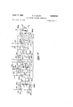
TRANSPARENT CONTAINER INSPECTION Filed Sept. 15, 1958 7 Sheets-Sheet 2 43 I o A April 1962 e. c. SEAVEY 3,030,516
TRANSPARENT CONTAINER INSPECTION Filed Sept. 15, 1958 L w w I "I o T 11/1 2;
7,? 147 10/ II K 94 PI Fl 1 jmhl- Hm j.
7 Sheets-Sheet 3 April 17, 1962 G. c. SEAVEY TRANSPARENT CONTAINER INSPECTION 7 Sheets-Sheet 4 Filed Sept. 15, 1958 April 17, 1962 G. c. SEAVEY TRANSPARENT CONTAINER INSPECTION '7 Sheets-Sheet 5 Filed Sept. 15, 1958 i54 ga /g 2W z V219 Kzu/ 1 41,.
A ril 17, 1962 G. c. SEAVEY TRANSPARENT CONTAINER INSPECTION 7 Sheets-Sheet 6 Filed Sept. 15, 1958 April 17, 1962 G. c. SEAVEY TRANSPARENT CONTAINER INSPECTION Filed Sept. 15, 1958 7 Sheets-Sheet 7 United States Patent Qfiice 3,930,516 Patented Apr. 17, .1962
This invention relates to inspection of transparent containers such as glass jars, and more particularly to apparatus and methods for detecting different types offiaws occurring in the walls of a container. Flaws are objectionable either because they may weaken a container, or because, in the eye of a discriminating buyer, they detract from the appearance of a packaged product and suggest that care was not taken in the manufacture of the product or its container.
For example, in the molding of a glass jar a single relatively large, horizontal lap or ridge may be formed on the wall of a jar. Or a series of fine ridges may be formed in a washboard pattern. According to previous methods a fine pencil of light directed on either imperfection will result in a scattering of light which may be detected as a serious flaw. However, a small washboard will not weaken or disfigure the jar as seriously as a horizontal lap. Therefore, it will not suffice to detect a flaw of the general class which includes, for example, washboards and horizontal laps.
Accordingly, it is an object of the invention to provide an inspection method and apparatus which will differentially detect specific types of flaws without regard to the presence of other types of imperfections-or similar but harmless imperfections or variations in container shape.
According to the invention a method of ditferentially detecting two or more types of flaws in the wall of a transparent container comprises projecting a narrow beam of light on the container, producing relative motion between the container and the beam thereby to scan the wall with the beam, flaws of different types diverting the beam .ondifferent predeterminable paths, preventing the light diverted on one path from substantially overlapping another path, and detecting the beam diverted on said one path, thereby to detect the beam diverted by one flaw independently of the other diverted beam.
Further, according to the invention a preferred inspection apparatus comprises optical means for projecting a narrow beam of light on the container, means producing relative motion between said container and optical means thereby to scan said wall with said beam, flaws of different types diverting the beam on different predeterminable paths, at least two photoelectric detecting means, each on a different path, and means for preventing light diverted to one detecting means from reaching the other detector. Still further according to the invention relative motion is produced between the container and projecting means, which motion is rotational about an axis and linear along said axis thereby repeatedly to scan the container wall with the beam, flaws of different types diverting the beam with different characteristics or modulations which are detected as corresponding electrical signals, and circuit means are connected to the aforesaid detecting ineans -whichpass only signals with selected characteristics or modulations, thereby difierentiatlly to detect one type of flaw.
For the'purpose of illustration a typical embodiment of the invention is shown in the accompanying drawing 'in which:
FIG. 1 is an isometric view of a jar illustrating several flaws;
FIG. 2 is a schematic view showing the method of detecting the several flaws;
FIG. 3 is a vertical section of an automatic jar feeding and inspectionmachine;
FIG. 4 is a partial top plan view of the machine of FIG. 3;
FIG. 5 is a partial underside view of the machine of FIG. 3;
FIG. 6 is a detail in elevation of the jar feeding machine;
FIG. 7 is an elevation, partly in section, o f-the electrooptical inspection station of the machine;
FIG. 8 is a plan view of the inspection station;
FIG. 9 is a section on line 9-9 of FIG. 8;
FIG. 10 is a section on line Iii-1410f FIG. '8;
FIG. 11 is a section on line 11-11 of FIG. '8;
FIG. 12 is a block diagram of the power supply for the electro optical inspection station; and
FIGS. 13 to 18 are schematic diagrams of the electronic circuits associated with the electro-optical inspection station.
FIGS. 1 and 2 illustrate five common undesirable imperfections in a glass jar] andt-he way in which they divert, that is reflect or refract, an incident light beam 1 or 2. The five flaws are a stone, a blister, ahorizontal lap, a washboard, and a vertical mark.
A stone is a small fragment of opaque material such as grey, unfused silica, embedded in or near the surface of the glass wall so as to form a lenticular area which reflects incident light through a wide angle (e.gf) including, for example, the path .9 of FIG. 2.
A blister is a superficial or internal 'air'bubble or defect causing a bulge in the'wall of the jarwhich acts as a lens or prism retracting light through a wide angle, the extent of which includes the path b. Light on the path I; is more intense than that which is transmitted by a stone, and scattered in a cone rather than in a horizontal or vertical Zone, as isthe'case with the following defects.
A horizontal lap is a single horizontal crease of varying length on theoutside of the wall. Acting like a cylindrical lens it retracts the incident beam on either or both of two small, vertical angles indicated by the paths 1. It will be understood that the terms vertical and horizontal are used with reference to a jar normally disposed as shown, and that other orientations are possible depending on the disposition of the jar. I
A washb'oa-rd is a series of several closely spaced external wrinkles each resembling a lap in that the incident light is weakly refracted into a vertical zone including two small vertical angles W. Thewashboard as .a whole however differs from a horizontal lap in that the wrinkles are repeated.
A vertical mark i's like a lap, but, as the termimplies,
vextends vertically or axially of .the container, and retracts light in ahorizontal zone including two small horizontal angles v. It differs from the vertical .mold seams in that these occur twice, apart on'the circumference of the container whereas the mark occurs only once or at random spacing.
Other minor defects such as constrictions at the neck of the container and variations in wall thickness will retract the incident beam with some scattering of the beam and must be distinguished from the five specific flaws.
In the feeding apparatus, shown in FIGS. 3 to 6, jars I are conveyed along a belt 31 to an entry star wheel 32 which rotates through a hood 33. The hood 33 covers a light-tight chute 34 into which the jars drop successively down to rubber rolls 36. The rolls are spaced sufficiently closely to arrest and grip each jar, and are inclined at a slight angle to the vertical to impart both a rotary and a downward motion to each jar. As shown in FIG. 3, the rolls 36 are driven by a collar 37 frictionally engaging the rolls and driven by a gear 38. The rolls may be driven by other means such as a gear drive. The rolls 36 spin the jars at about 2000 rpm. and feed them downward at about 0.05 inch per revolution so that somewhat less than 50 jars per minute are fed through the rolls. Of course, the jars may be driven at faster or slower rates of spin and linear feed as may be desirabletion station the flaws are detected and resultant electronic signals transmitted to amplifying and control circuits 43.
After passing the rolls the jars drop onto a cushion 44 on a base 45 at the bottom of the chute and within an exit star wheel 46. The exit star wheel carries the jars past a rejection mechanism, shown for simplicity as a trap door in the base 45, and thence to a belt conveyor 48. The amplifier circuits 43 control a time delay device 49 which allows for the transit time between the rolls 36 and the trap door 47, so that when a jar with a detected defect reaches the trap door, the time delay device permits energization of a relay 50 controlling the trap door or other rejection device. Jars having defects detected at the inspection station are thus removed from the series delivered to the exit conveyor 48.
The inspection station at the spin rolls is shown schematically in FIG. 2 and FIGS. 7 to 11. Briefly described, it comprises a primary light source X1 directing a thin light beam 1 on the jar I, from which the beam may be diverted on the previously mentioned paths s (stone), b (blister), 1 (lap) and v (vertical line) respectively leading to one or two photocells. The photocells, meaning to include tubes as well as semi-conductor devices, are respectively Vs (stone), Vb (blister), VII and V12 (lap) and Vv (vertical line), each connected to an amplifier circuit which will be described in detail. In addition, a. ray 2 is reflected directly back on the path 1 to a semireflector 51 at 45 to the path e, and is there reflected to an enable photocell Ve. Reflection on the path e occurs only when the primary pencil 1 strikes a vertical wall of the jar. The non-vertical neck and bottom portions are ignored. 7
Primary Light Source X1 As shown in FIGS. 7 and 8, the primary light source is a lamp 52 enclosed in a ventilated housing 53 secured to the chassis 42. Opposite the lamps filament is a lens barrel with lenses and masking slits whichdirect on the jar a collimated light beam. The light spot formed by the beam on the jar may have, for example, a vertical length of 0.10 inch parallel to the axis of the jar, and a horizontal width of 0.03 inch. Since the jar is fed 0.05 inch per revolution, the helical band scanned during one revolution slightly overlaps the subsequent band insuring that the entire vertical surface is scanned. The end of the lens barrel is located about 1 inches from the verticalwall of the'jar. V V
4 Power Supply In FIG. 12 is shown a conventional 115 v. input power supply having DC. output voltages A, B, C, and D, negative with respect to ground E, and DC. output voltages F, G, and H positive with respect to ground E, and filament voltages X, Y, and Z. The approximate voltages with respect to ground E are: A, 700, B, 550, C, -400, D, -250 F, +75, G, +150, H, +300. Any of voltages A to D may be used to supply the dynodes of the phototubes, the choice depending on the desired sensitivity. Voltages F to H are used to supply the operating voltages for the electronic tubes of the detectors. In addition, G supplies the anodes of the phototubes. Filament voltages X, Y, and Z are all approximately 6.3.
The Enable Function As previously mentioned, the vertical sidewall of the jar reflects an intense beam from the jar directly back on the incident beam 1 to a reflector 51 and thence on a path e. Light on path e is admitted through an aperture 56 to a housing 54 at the edge of the chute and causes the photocell Ve to respond by high conduction when the vertical jar wall is scanned by the incident beam 1. The gross departures from the vertical at the jar neck and bottom scatter the light so that the photocell response drops radically.
The output of the photocell Va is applied to an enable amplifier shown in FIG. 13. In this figure, as in FIGS. 14 to 18, typical values of the resistive and capacitative circuit elements are shown where the elements are not identified by reference characters, and connections to external circuits are identified by lettered arrowheads or terminal symbols.
A current signal from the enable photocell V2 is taken from its last dynode d9 and applied to the control grid of one half of a type 12AT7 tube V11, normally biased below cutoff by a voltage divider comprising a 27K resistor and a 5K potentiometer.
The following stage V12 is also one half of a type 12AT7 tube but is normally conducting by virtue of positive bias obtained from the 150 volt positive terminal G 'of the powersupply. Stages V11 and V12 are coupled through a condenser C11, which is normally charged to 150 volts, or the potential diiference between G and H of the power supply. The signal causes stage V11 to conduct which in turn causes the grid of stage V12 to go negative. Condenser C11 will slowly discharge through the 1 megohm adjustable resistor R11 until the grid of stage V11 again reaches a potential where it will conduct. The values of C11 and R11, e.g. l microfarad and 1 megohm respectively, are such as to hold the control grid of stage V12 negative for only the approximately 1 seconds time required to scan the vertical jar wall, even though stage V11 will be conducting for the somewhat longer time required for the neck of the jar also to pass through the light beam. The function of diode D2 is to quickly charge condenser C11 as soon as stage V11 ceases to conduct.
The following stage V13, one half a type 12AT7 tube, is normally cut ofi by conduction of stage V12, and when stage V12 is cut ofi, the voltage at the control grid of 7 stage V13 rises abruptly causing stage V13 to reach maximum conduction. Stage V13 is in series with the positive voltage terminal H and a plate supply terminal I for each of the other photocells shown in FIG. 14.
Terminal I is normally at approximately volts positive'by virtue of its connection to supply terminal F through the two 47 kilohm resistors, and this is the voltage appearing at the anodes of each of the phototubes Vs. Vb, V11, V12, Vwl, and Vw2. The dynode d9 of each of these .tubesis at a higher potential by virtue of being connected to supply terminal G. Hence no current will flow from the anode to the dynode d9. When stage V13 conducts, the voltage atterminal I becomes more positive bringing the anode voltage of each'phototube above that of the last dynode.
A filter in the output circuit comprising a 47 ki-lohm resistor R12 and a .22 microfarad capacitor C12 prevents a rapid rise of voltage at terminal I which otherwise would cause a pulse which the detector photocells might detect as a flaw. The function of diode D1 (1N461) is to hasten the discharge of the .22 microfarad capacitor at the end of the scanning-period.
The flaw detecting photocells, shown in FIG. 14, are type 931A, having an anode a, nine dynodes d1 to d9 and a cathode k. The anode voltage controlled by the enable circuit of FIG. 13 is applied in each case through a 220 kilohm resistor. Each photocell has a conventional voltage divider connectedbetween the 150 volt positive supply terminal G and the 700 volt negative supply terminal A to provide voltage steps of approximately 85 volts per stage, the cathode in each case being connected to the 700 volt negative terminal A. The photocells Vs, Vb, Vv, V11, V12, Vwl and Vw2 have output terminals 11 to 7 respectively.
From theforegoing description, it is apparent that the several photocells can apply no signal to their respective output terminalsunless the vertical wall of the jar has activated the enable circuit and caused it to supply anode voltage to the anodes of the flaw-detecting photocells.
Stone Detection As shown in FIGS. 2, 8 and 10, the llenticular area caused by an embedded stone causes reflection of the incident light beam 1 on a wide angle including the path s leading to the stone-detecting photocell Vs. The photocell Vs is enclosed in a housing 61 on the chassis 42. The housing carries a short barrel extending from the photocell Vs and terminating in a member 62 forming an aperture 63 about lf-, in diameter. The axis of the barrel is on the path s at an angle of about 40 to the incident light beam 1, and the aperture is disposed close (about one-half inch) to the jar J, the photocathode of the photocell Vs being about 1 /2 inches from the jar. While other defects will cause some reflection, it will not be so intense at angles such as that ofthe path s. Substantial reflection from parts of the jar other than the spot being scanned is avoided by the location of the small aperture 63 close to the jar.
When the incident beam 1 strikes a stone, a short flash of light is reflected on the photocell Vs whose associated circuit is shown in FIG. 15. Momentary conduction of the photocell Vs applies a short negative pulse through its output terminal ii to the first stage V21 of a conventional two-stage, resistance, capacitance coupled amplitier. The first and second stages V21 and V22 each comprise one-half a type 12AT7 tube. Stage V21 is normally conducting and stage V22 is normally cut oflt' by positive cathode voltage supplied by current from power terminal F flowing through a 100K cathode resistor. he negative pulse initiated by a flaw is applied to the control grid ofstage V211 and cuts off the first stage, which then applies a positive pulse to the control grid of the second stage V22 causing it to conduct. On conduction, negative swing of voltage at the anode of stage V22 is coupled through a 0.5 rnicrofarad capacitor C21 to the control grid of the first-stage V21 thereby length ening thetirne which stage V21 is cut offand stage V22 conducts to about second. In series with the second stage V22. is a relay K1 which is held energized for, this time. The relay contacts complete circuits through an indicator lamp V23 and control terminals S. The control terminals 5 are connected to the time delay .49 which activates the rejection device 47 at the bottom of the inspection chute (FiGS. 3 and 5). Like relay contacts of the flaw-detection circuits to be described are connected in parallel with the control terminals S of the stonedetection amplifier. Thus, on detection of any of the stone or other described flaws, the rejection device "will be actuatedwhen the defective jar has arrived at the rejection device.
Blister Detection As shown in FIGS. 2, 7, 8 and 9, the photocell Vb for detecting blisters is located approximately 23 to one side and 30 above a projection of the incident beam 1. In this position, the photocell is within the cone of intense light refracted forwardly bythe lense effect of the small air bubble defect. As previously mentioned, a stone primarily reflects while a horizontal lap, vertical line or washboard primarily retract in a relatively narrow horizontal or vertical zone. Thus, the path b on which the beam is refracted by a blister lies outside the refraction paths of the vertical and horizontal defects, andpath b receives very little light by refraction from a stone or from minor defects.
As in the case of a stone, a blister directs a momentary flash of light on the blister-detecting photocell Vb causing it to conduct momentarily. Associated with the photocell Vb is an amplifier circuit like that of 'FIG. 15. Again a short pulse is amplified and stretched to hold a control relay energized for approximately /5 second and apply a signal to the time delay.
Horizontal Lap Detection As shown in FIGS. 2, 7, 8 and 9, a horizontal lap primarily retracts the incident beam both upwardly and downwardly in a vertical zone with relatively little horizontal spread, and is best detected by two vertically spaced photocells VII and VIZ. The photocells lie on two folded paths 1 which originate within the vertical zone and which are bent up and down by parabolic mirror surfaces 71 and 72. The mirror surfaces are masked from light deflected byother flaws by a plate 73 secured to a bracket 75 upstanding from the chassis 42. The plate 73 has two vertically spaced apertures 74 lying on the paths 1 and passing primarily only light deflected by a horizontal lap, so that the vertically deflected'beams will strike both of the lap-detecting cells V11 and V1.2. By way of example, the mask 73 may lie approximately 2 inches from the center line of the jar. The apertures are spaced about /2 inch apart and are approximately 0.1 inch in height and A inch in width.
The lap photocells V111 and Vl2 are connected to an amplifier circuit shown in FIG. 18. The circuitrequires that each photocell must receive light above a certain intensity and that the sum or average of the two must exceed a predetermined minimum before the circuit will cause a rejection of the jar under test.
The respective lap photocells, when caused to conduct by a light pulse, apply negative pulses to the control grids of amplifier stages V81a and Vfilb, each one half a type 6SN7 tube. The pulses are integrated by networks RG81 and RG82 which discriminate between long laps and short laps, the networks passing only long lap signals. The stages V81a and V8112 are adjusted for normal conduction at the same level by 2 megohmpotentiometers. When cut ofl by the long lap pulse, they apply a positive voltage to the control grids of stages V82a and 'V82b, each comprising one-half of a 6SL7 tube normally biased below cutoff by a cathode biasing, K potentiometer R85, by means of which the threshold may be adjusted. Diodes D81 and D82 (type 1N461) serve as. DC restorers for the bias circuit.
The two negative outputs at the anodes of the stages V82a and V821) are averaged by 1.2 megohm resistors R83 and R84 and the resultant mean pulse applied to the control grid of stage V83a, one-half a type 6SL7 tube normally conducting at saturation. The circuit con stants are such that this stage will not operate below cutofi unless both of stagesV82a and V821; are conducting. If stage V83a is cut off, a sub-sequent stage 'V84a is allowed to conduct.
Stage V84a is in series -witha control relay K81 and '7 a stage V8412, both V84a and V841) being one half of a type 12AT7 tube. Both halves must conduct to energize the relay. The second half V84b is caused to conduct by cutofi of the input stages V8111 and V8121. The
resultant positive swing at the anodes of stages V81a and V81b is applied through averaging resistors R81 and R82, each 1 megohm, and the combined signal applied to the control grid of stage V34b.
V rtical Line Detection Vertical lines or marks are detected by the apparatus and circuit shown in FIGS. 2, 7, 8 and 9. The incident beam 1 is spread by the mark primarily in a horizontal zone with a vertical width so small that appreciable light from the mark does not extend upwardly to the apertures which admit light from a horizontal lap. However, the horizontal spread of the zone is sufiicient so that paths v pass to either side of the approximately 1 inch wide mask 73. Beyond the mask 73 are reflectors 91 and 92 converging on an aperture 93 in an upright plate 94. The reflectors 91 and 92 are preferably curved as shown in FIG. 9, but may be planar as shown schematically in FIG. 2. These reflectors bend the light paths v so that they pass through the aperture to the vertical mark-detecting photocell Vv. Only light momentarily deflected right or left causes the photocell to conduct.
The associated circuit is shown in FIG. 16. The negative pulse at the anode of the photocell Vv is applied through a resistor-capacitor network RG91 to the grid of an input stage V91, one half of a type 6SL7 tube, normally conducting as a conventional linear amplifier. The network RC91 comprising two 1 megohm resistors R91 and R92 and a .091 microfarad capacitor C91 filters out low frequency signals such as might be caused by ordinary variation in thickness of the jar wall. On the other hand, the network passes pulses of short rise time such as are caused by the momentary refraction of a vertical mark.
The amplified output of the input stage V91 is coupled through a tuned circuit RG92 which serves to accentuate the rotational frequency of the jar and hence of the vertical mark pulses. The network thus discriminates against similar pulses caused by the two vertical mold marks, which pulses occur at twice the frequency of the vertical mark pulses. Further, the tuned network accentuates the sharpness of the mark pulses so that the out of phase mold pulses are subtractive rather than spuriously additive.
The sharpened negative pulse is applied to the grid of the second stage V92, one half a type 6SN7 tube. The second stage V92 is a linear amplifier whose sensitivity is adjusted by a 150 kilohm potentiometer at the anode of stage V91. A resonant circuit LC91 in the cathode circuit comprises an inductance L91, commercially available as Freed No. QGC4 and having an inductance of approximately 25 henries, and an adjustable capacitor C91 having a capacitance of approximately 1 microfarad. The resonant frequency of this circuit is tuned to the frequency of the mark pulses. Signal voltage for the following stage is taken from across this tuned circuit,
. frequencies other than the mark frequency being thus effectively filtered out. The third stage V93, one half a 6S-L7, amplifies linearly the filtered signal and applies positive feed-back to the grid of the preceding stage V92 through a feed-back loop RG93. The level of feedback may be adjusted by a 150 kilohm potentiometer 1n th e anode circuit of stage V93; The positive feed-back '8 stretches the pulses and increases the selectivity of the resonant circuit RCL91.
The pulse signal is also applied from the anode of stage V93 to a conventionallinear amplifier V94. The cathode output of stage V94 is applied through a pulse transformer T91, available as Triad No. A401, to full wave rectifiers D92 and D93, type 1N46l diodes. The rectified pulse signal is integrated in a network RG94 including a type 1N46l diode D94. The network integrates the resulting positive pulse series so as to discriminate against short series of pulses representing a short and harmless vertical mark. The diode removes any negative swing of the resultant long positive pulse which is applied to the grid of the final stage V95. The final stage, a type 6SL7 tube, is biased below cutoff by a ohm potentiometer in the cathode circuit, and conducts only on a positive pulse passed by the network RG94. Thus, only a vertical mark of substantial length can trigger the final stage and energize the control relay K91.
Washboard Detection A washboard comprising a series of parallel horizontal lenticules scatters light in a vertical zone similarly as does a single horizontal lap, but difiers in that the scattering occurs in a number of successive revolutions of the jar.
As shown in FIGS. 2, 7 and 8, a separate source X2 of colored or filtered light directs a secondary scanning beam 2 on the jar J. While the primary source X1 may be used to scan a washboard and the reflected beam and resultant signal differentiated optically from a lap, preferably the two sources X1 and X2 emit light in different portions of the light spectrum from ultraviolet through visible to infrared light. For example, source X1 may project a filtered orange-yellow light, and source X2 2. blue-violet light. As in the case of a horizontal lap, two paths w define the angle within which the washboard reflects light both upwardly and downwardly. The paths w pass through a blue-violet filter 191 which transmits substantially only the light of the source X2. Thus when source X1 is of a different color than that passed by the filter, light from source X1 which is reflected by flaws or irregularities will be rejected by the filter. If the secondary source X2 emits ultraviolet (source X1 emitting only visible light), such light will be reflected only from outside surface flaws, and other flaws inside the jar will not thereby be detected.
As shown in FIGS. 7, 8 and 11, the washboard-detecting photocells Vwl and Vw2 are mounted one above the other in a housing 1&2. Opposite the jar I is a frame 103 holding the filter 101. Within the housing and between the photocells is a block 104 having parabolic reflecting surfaces 1636 and 107. A beam on one of the general paths w is reflected upwardly to photocell Vwl and the other downwardly to photocell VWZ.
The washboard detection circuit of FIG. 17, like the lap circuit of FIG. 18, operates to reject a jar only when both photocells conduct during several revolutions, that is, when the area of the washboard is substantial.
The first two 6SL7 stages V101aV101b and 1102a- V102b of the washboard amplifier are identical with those of the lap detector of FIG. 18. The two photocell signals applied .to the input stages are integrated and amplified, and the output of both the first and second stages are averaged. The negative averaged output of the second stage V1(l2aV1tl2b is applied to a normally conducting third stage V163, one half a type 12AT7 tube, causing this stage to be cut 011 and to apply a positive pulse to the grid of the subsequent stage V104a,
one half a type l AT7 tube. This stage V1ll4a is in series with a like stage V1941) and the primary of a pulse transformer T101. Vxhen both normally cutofi series stages V104a and V1041 conduct, voltage developed 'the rate of rotation of the jar.
as to FIG. 16. The final normally cutoff stage V105,
one half a 12AT7, supplies current to the control relay K101, whose switching contacts are in parallel with all of the previously described relay contacts.
Summary From the foregoing detailed description of the optical inspection apparatus and associated circuits, it can be seen that the present invention differentially detects light diverted in particular ways from particular flaws and ignores light diverted from inconsequential imperfections or light diverted with low intensity from a particular flaw. For example, intense light reflected in a solid angle from a stone can be differentiated by masking light from other flaws which is not intense in the solid angle. Where light is refracted in a horizontal zone by a mark, or in a vertical zone by a lap, rather than the conical zone of a blister, the middle parts of the long, narrow zones may be masked and light passing through both ends of the zone will be peculiar to the horizontal or vertical flaw and of greater intensity than that from the blister.
Further the size and repetitive characteristics of vertical marks and washboards may be used to distinguish them from other flaws and minor defects by selection of modulation characteristics. In the case of the washboard flaw it is preferable to use a different colored light ther a flaw like a vertical mark may be repeatedly scanned as the jar is fed downwardly so as to modulate the scanning beam with a repetition rate or frequency equal to A signal with a particular repetition rate can also be selected electronically.
It should be understood that the present disclosure is for the purpose of illustration only and that this invention involves all modifications and equivalents which fall within the scope of the appended claims. For example, while helical scanning is shown and described other scanning patterns may be employed.
What is claimed is:
1. The method of difierentially detecting one of two or more types of flaws in the wall of a transparent container at a station, comprising projecting a narrow beam of light on the container, producing relative motion between said container and the beam thereby to scan said wall with saidbeam, flaws of different types diverting the beam on different predeterminable paths, preventing the light diverted on one path from overlapping the other path, and detecting the beam on said one path at said station, thereby to detect one diverted beam independently of the other.
2. The method of differentially detecting one of two or more types of flaws in the wall of a transparent container at a station, comprising projecting a narrow beam of light on the container, producing relative motion between said container and the beam thereby to scan said wall with said beam, flaws of different types diverting the beam on different predeterminable paths, preventing the light diverted on one path from overlapping the other path, and detecting the beams on the different paths at said station, thereby to detect each diverted beam independently.
3. The method of differentially detecting'one of two or more types of flaws in the wall of a transparent container at a station, comprising projecting a narrow beam of light on the container, producing relative motion between said container and the beam thereby-to scan said Wall with said beam, flaws of different types diverting the beam on different predeterminable paths, the paths from one flaw lying primarily in one zone and the paths from another flaw lying within and primarily without said zone, and detecting only light lying on a-path within said zone at said station, thereby to detect'one diverted beam independently of the other.
4. The method of differentially detecting one oftwo or moretypes of flaws in the wall of a transparent container at a station, comprising'projecting a narrow beam of light on the container,:producing relative motion between said container and the beam-thereby to scan said wall with said beam, fiaws of different types diverting the beam on different predeterminable paths, the paths from one flaw lying primarily within a solid angle and the paths from another flaw lying within and primarily Without said angle, obstructing light on'paths outside said solid angle and detecting only light lying on a-path within said angle at said station, thereby to detect one diverted beam independently of the other.
5. The method of differentially detecting one of two or more types of'flaws in the wall of a transparent container at a station, com-prising projecting a narrow beam of light on the container, producing relative motion between said container and the beam thereby to scan-said wall with said beam, flaws of different types diverting the beam on diiferent-predeterminable paths, the paths from one flaw lying primarily within a zone having a long, narrow cross section andthe paths from another flaw lying within and primarily without said zone, obstructing light on paths through the middle and outside said zone, and detecting only light lying on'two paths passing through the ends of said zone at said station, thereby to detect light from one flaw independently of light from the other;
6. The method of differentially detecting one of two or more types of flaws in the wall of a transparent container at a station, comprising projecting two narrow beams of light on the container, producing relative motion between said container and the beams thereby to scan said wall with said beams, flaws of different types diverting the beams on ditferent'predeterminable paths, preventing the light of one diverted beam from overlap ping light of the other diverted" beam, and detecting only the light of one diverted beam at said station, thereby to detect one flaw independently of the other.
7. The method of differentially detecting one of two or more types of flaws-in the wall of a transparent container at a station, comprising projecting a narrow beam of light on the container, producing relative-motion between said container and the beam therebyto scan said Wall with said beam, fiawsof different types diverting the beam .on different predeterminable paths'with different modulation characteristics, preventing thelight diverted on one path from substantially overlapping the other path, detecting the beam on said one path at said station thereby to produce an electric signal havinglsaid different modulation characteristics, and selecting only that part of the signal having a particular modulation characteristic, thereby to detect one .flaw independently of the other.
8. Inspection apparatus for'differentially detecting one of two or more types of flaws. in the wall of a transparent container at a station, comprising optical'means forprojecting a narrow beam of light on the container, means producing relative motion between said container and optical means thereby to scan said wall with said beam, flaws of different types divertingthe beam on difierent predeterminable paths,. at least two I photoelectric detect- 1 1 masking means in at least two of said paths passing light on only one path preventing light diverted to one detecting means from reaching the other detecting means.
9. Inspection apparatus for differentially detecting one of two or more types of flaws in the wall of a transparent container at a station, comprising optical means for pro jecting a narrow beam of light on the container, means producing relative motion between said container and optical means thereby to scan said wall with said beam, flaws of different types diverting the beam on predeten minable paths in different overlapping zones, photoelectrio detecting means in one of said zones at said station, and means masking the over-lapping portion of said zones and passing light primarily only in one zone thereby to prevent light in another zone from reaching the detecting means in said one zone, so that the detecting means in said one zone detects a particular flaw.
10. Inspection apparatus for differentially detecting one of two or more types of flaw-s in the wall of a transparent container at a station, comprising optical means for pojecting a narrow beam of light on the container, means producing relative motion between said container and optical means thereby to scan said wall with said beam, flaws of different types diverting the beam on different predeterminable paths, the light paths from one flaw lying primarily in a zone having a long narrow cross section, means masking all but the ends of said zone, and photoelectric detecting means beyond said ends respectively at said station, and circuit means responsive only when light falls on both of said photoelectric means.
11. Inspection apparatus :for detecting one of two or more types of flaws in the wall of a transparent container at a station, comprising means for projecting a narrow beam of light on the container wall, means producing between said container and projecting means relative rotational motion about an axis and relative linear motion along said axis thereby repeatedly to scan said wall with said beam, flaws of different types diverting said beam with modulations of diiferent characteristics, photoelectric detecting means in one of said paths at said station for converting beam modulations into electrical signals of like characteristic, and circuit means connected to said detecting means including means selecting only signal modulations of one characteristic, thereby diiferentially to detect one type of flaw, and means utilizing said selected signal to identify a container with a flaw.
12. Inspection apparatus for diiferentially detecting one of two or more types of flaws in the wall of a transparent container at a station, comprising optical means for projecting a narrow beam of light on the container, means producing relative motion between said container and optical means thereby to scan said wall with said beam, flaws of diiferent types diverting the beam with modulation of different characteristics, photoelectric detecting means in one of said paths at said station for producing an electrical signal with characteristics like that of the diverted beam, circuit means connected to said detecting means including means selecting only a signal of one characteristic thereby difierentially to detect one type of flaw, and means utilizing the selected signal so as to identify a container having a flaw. 7
13. Inspection apparatus for difierentially detecting one of two or more types of flaws in the wall of a transparent container at a station, comprising optical means for projecting a narrow beam of light on the container, means producing relative motionbetween said container and optical means thereby to scan said wall with said beam, flaws of different types diverting the beam with modulation of different rise times, photoelectric detecting means in one of said paths at said station for producing an elec trical signal with a rise time dependent on that of the diverted beam, circuit means connected to said detecting 7 means including means selecting only a signal of short rise time thereby differentially to detect one type of flaw,
12 and means utilizing the selected signal so as to identify a container having a flaw.
14. Inspection apparatus for differentially detecting one of two or more types of flaws in the wall of a transparent container at a station, comprising optical means for projecting a narrow beam of light on the container, means producing relative motion between said container and optical means thereby repeatedly to scan said wall with said beam, flaws of one type repeatedly modulating said beam at the scanning repetition rate, photoelectric detecting means in one of said paths at said station for producing an electrical signal with the same and other repetition rates, circuit means connected to said detecting means including means selecting only a signal of a particular repetition rate thereby differentially to detect one type of flaw, and means utilizing the selected signal so as to identify a container having a flaw.
15. Inspection apparatus for differentially detecting one of two or more types of flaws in the wall of a transparent container at a station, comprising optical means for projecting a narrow beam of light on the container, means producing relative motion between said container and optical means thereby repeatedly to scan said wall with said beam, flaws of one type repeatedly modulating said beam during an interval, photoelectric detecting means in one of said paths at said station for producing an electrical signal with characteristics like that of the diverted beam, circuit means connected to said, detecting means including integrating means selecting only a signal repeated for a predetermined interval diiferentially to detect large flaws of one type, and means utilizing the selected signal so as to identify a container having a large flaw.
16. Inspection apparatus for differentially detecting one of two or more types of flaws in the wall of a transparent container, comprising optical means for projecting a narrow beam of light on the container, means producing relative motion between said container and optical means thereby to scan said wall with said beam, flaws of different types diverting the beam with modulation of different characteristics, photoelectric detecting means in one of said paths for producing an electrical signal with characteristics like that of the diverted beam, circuit means connected to said detecting means including at least two successive amplifier stages and two electronic control valves in series with a control relay, respective amplifiers being connected to and separately controlling said control valves, and means controlled by said relay to identify a container having a fiaw.
17. Inspection apparatus for difierentially detecting one of two or more types of flaws in the wall of a transparent container, comprisingoptical means for projecting a narrow beam of light on the container, means producing relative motion between said container and optical means thereby to scan said wall with said beam, flaws of different types diverting the beam with modulation of different characteristics, photoelectric detecting means in one of said paths for producing an electrical signal with characteristics like that of the diverted beam, circuit means means connected to said detecting means including means selecting only a signal of one characteristic thereby differentially to detect one type of flaw, said circuit means including an amplifier channel having at least two ampliiier stages and a positive feedback circuit between said 7 stages, and relay means energized by said signal so as to identify a container having a flaw, said feedback lengthening the interval of said signal thereby to hold said relay means energized for a predetermined period.
18. Apparatus according to claim 17 characterized by a resonant circuit connected between said amplifiers for selecting signals of a predetermined signal, said feedback circuit increasing the selectivity of said resonant circuit.
19. Inspection apparatus for diiferentially detecting one 13 of two or more types of flaws in the wall of a transparent container, comprising optical means for projecting a narrow beam of light on the container, means producing relative motion between said container and optical means thereby to scan said wall with said beam, flaws of difierent types diverting the beam on different paths, two photoelectric detecting means in one of said paths for producing two electrical signals whose amplitude is dependent on the diverted beam, circuit means connected to respective detecting means, said circuit means including two amplifying channels respectively connected to said detecting means and a network for averaging the signals of the two channels, and relay means coupled to said network including means responsive only when both signals exceed a predetermined amplitude.
References Cited in the file of this patent UNITED STATES PATENTS 1,940,882 Rich Dec. 26, 1933 2,132,447 Stout Oct. 11, 1938 2,318,856 Hoffman May 11, 1943 2,454,411 Stoate Nov. 23, 1948 2,524,929 Razek Oct. 10, 1950 2,531,529 Price Nov. 28, 1950 2,593,127 Fedorchak Apr. 15, 1952 2,868,061 Fedorchak et a1. Jan. 13, 1959
Priority Applications (1)
| Application Number | Priority Date | Filing Date | Title |
|---|---|---|---|
| US761158A US3030516A (en) | 1958-09-15 | 1958-09-15 | Transparent container inspection |
Applications Claiming Priority (1)
| Application Number | Priority Date | Filing Date | Title |
|---|---|---|---|
| US761158A US3030516A (en) | 1958-09-15 | 1958-09-15 | Transparent container inspection |
Publications (1)
| Publication Number | Publication Date |
|---|---|
| US3030516A true US3030516A (en) | 1962-04-17 |
Family
ID=25061345
Family Applications (1)
| Application Number | Title | Priority Date | Filing Date |
|---|---|---|---|
| US761158A Expired - Lifetime US3030516A (en) | 1958-09-15 | 1958-09-15 | Transparent container inspection |
Country Status (1)
| Country | Link |
|---|---|
| US (1) | US3030516A (en) |
Cited By (21)
| Publication number | Priority date | Publication date | Assignee | Title |
|---|---|---|---|---|
| US3199401A (en) * | 1959-11-02 | 1965-08-10 | Pittsburgh Plate Glass Co | Method and apparatus for optically detecting elongated defects in glass |
| US3322024A (en) * | 1961-09-11 | 1967-05-30 | Ford Motor Co | Optical method for the inspection of a transparent object for deffects including comparing light energy at two stations |
| US3348049A (en) * | 1964-12-31 | 1967-10-17 | Ball Brothers Res Corp | High speed ultraviolet thin spot detector |
| US3356853A (en) * | 1965-01-04 | 1967-12-05 | Owens Illinois Glass Co | Radiation sensitive apparatus for inspecting the bottom wall of hollow transparent containers |
| US3361025A (en) * | 1960-12-13 | 1968-01-02 | Saint Gobain | Method and apparatus of detecting flaws in transparent bodies |
| DE1286783B (en) * | 1963-10-21 | 1969-01-09 | Owens Jllinois Inc | Testing device for determining material defects in radiation-permeable containers |
| US3438492A (en) * | 1967-02-17 | 1969-04-15 | Owens Illinois Inc | Bird swing detector |
| US3439178A (en) * | 1965-02-08 | 1969-04-15 | Owens Illinois Inc | Radiation-sensitive apparatus for inspecting wall thickness of hollow containers |
| US3629595A (en) * | 1970-03-11 | 1971-12-21 | Barry Wehmiller Co | Transparent container inspection apparatus |
| US3639067A (en) * | 1970-06-29 | 1972-02-01 | Emhart Corp | Glassware inspection apparatus employing fiber-optic guides |
| DE1573739B1 (en) * | 1965-09-13 | 1972-03-09 | Owens Illinois Inc | PROCEDURE AND DEVICE FOR SIMULTANEOUSLY CHECKING GLASS CONTAINERS WITH ROUNDED UPPER EDGES FOR VERTICAL IRREGULARITIES IN THE EDGES AND FOR DEFECTS IN THE BASE AREA |
| DE1573738B1 (en) * | 1966-06-30 | 1972-04-27 | Owens Illinois Inc | DEVICE FOR DETECTING CRACKS AND SIMILAR DEFECTS IN THE SURFACE OF GLASS CONTAINERS |
| US3662883A (en) * | 1970-12-07 | 1972-05-16 | Owens Illinois Inc | Bird swing detector |
| US3814946A (en) * | 1972-12-04 | 1974-06-04 | Asahi Glass Co Ltd | Method of detecting defects in transparent and semitransparent bodies |
| US3988068A (en) * | 1974-05-09 | 1976-10-26 | Itek Corporation | Method and apparatus for detecting cosmetic defects in opthalmic lenses |
| US4601395A (en) * | 1984-04-23 | 1986-07-22 | Owens-Illinois, Inc. | Inspecting and sorting of glass containers |
| US6104482A (en) * | 1999-12-02 | 2000-08-15 | Owens-Brockway Glass Container Inc. | Container finish check detection |
| US7010863B1 (en) | 2004-01-26 | 2006-03-14 | Owens-Brockway Glass Container Inc. | Optical inspection apparatus and method for inspecting container lean |
| US7148961B1 (en) | 2004-11-10 | 2006-12-12 | Owens-Brockway Glass Container Inc. | Container sidewall inspection |
| US20070035820A1 (en) * | 2004-11-24 | 2007-02-15 | Battelle Memorial Institute | Sample tube handling apparatus |
| US8941825B2 (en) | 2013-03-15 | 2015-01-27 | Owens-Brockway Glass Container Inc. | Container inspection |
Citations (8)
| Publication number | Priority date | Publication date | Assignee | Title |
|---|---|---|---|---|
| US1940882A (en) * | 1930-07-30 | 1933-12-26 | Westinghouse Electric & Mfg Co | Sorting apparatus |
| US2132447A (en) * | 1935-02-05 | 1938-10-11 | Coca Cola Co | Process and apparatus for inspecting fluids |
| US2318856A (en) * | 1941-03-01 | 1943-05-11 | Fed Cartridge Corp | Inspecting device |
| US2454411A (en) * | 1939-09-07 | 1948-11-23 | United Dairies Ltd | Inspection apparatus for transparent vessels |
| US2524929A (en) * | 1946-02-21 | 1950-10-10 | Wm S Scull Company | Photoelectric method and apparatus for testing vacuum conditions in containers |
| US2531529A (en) * | 1949-09-30 | 1950-11-28 | Rca Corp | Inspection apparatus and method |
| US2593127A (en) * | 1950-01-24 | 1952-04-15 | Owens Illinois Glass Co | Electronic inspection of glass containers |
| US2868061A (en) * | 1954-10-26 | 1959-01-13 | Owens Illinois Glass Co | Inspection of glassware by radiation |
-
1958
- 1958-09-15 US US761158A patent/US3030516A/en not_active Expired - Lifetime
Patent Citations (8)
| Publication number | Priority date | Publication date | Assignee | Title |
|---|---|---|---|---|
| US1940882A (en) * | 1930-07-30 | 1933-12-26 | Westinghouse Electric & Mfg Co | Sorting apparatus |
| US2132447A (en) * | 1935-02-05 | 1938-10-11 | Coca Cola Co | Process and apparatus for inspecting fluids |
| US2454411A (en) * | 1939-09-07 | 1948-11-23 | United Dairies Ltd | Inspection apparatus for transparent vessels |
| US2318856A (en) * | 1941-03-01 | 1943-05-11 | Fed Cartridge Corp | Inspecting device |
| US2524929A (en) * | 1946-02-21 | 1950-10-10 | Wm S Scull Company | Photoelectric method and apparatus for testing vacuum conditions in containers |
| US2531529A (en) * | 1949-09-30 | 1950-11-28 | Rca Corp | Inspection apparatus and method |
| US2593127A (en) * | 1950-01-24 | 1952-04-15 | Owens Illinois Glass Co | Electronic inspection of glass containers |
| US2868061A (en) * | 1954-10-26 | 1959-01-13 | Owens Illinois Glass Co | Inspection of glassware by radiation |
Cited By (28)
| Publication number | Priority date | Publication date | Assignee | Title |
|---|---|---|---|---|
| US3199401A (en) * | 1959-11-02 | 1965-08-10 | Pittsburgh Plate Glass Co | Method and apparatus for optically detecting elongated defects in glass |
| US3361025A (en) * | 1960-12-13 | 1968-01-02 | Saint Gobain | Method and apparatus of detecting flaws in transparent bodies |
| US3322024A (en) * | 1961-09-11 | 1967-05-30 | Ford Motor Co | Optical method for the inspection of a transparent object for deffects including comparing light energy at two stations |
| DE1286783B (en) * | 1963-10-21 | 1969-01-09 | Owens Jllinois Inc | Testing device for determining material defects in radiation-permeable containers |
| US3348049A (en) * | 1964-12-31 | 1967-10-17 | Ball Brothers Res Corp | High speed ultraviolet thin spot detector |
| US3356853A (en) * | 1965-01-04 | 1967-12-05 | Owens Illinois Glass Co | Radiation sensitive apparatus for inspecting the bottom wall of hollow transparent containers |
| US3439178A (en) * | 1965-02-08 | 1969-04-15 | Owens Illinois Inc | Radiation-sensitive apparatus for inspecting wall thickness of hollow containers |
| DE1573739B1 (en) * | 1965-09-13 | 1972-03-09 | Owens Illinois Inc | PROCEDURE AND DEVICE FOR SIMULTANEOUSLY CHECKING GLASS CONTAINERS WITH ROUNDED UPPER EDGES FOR VERTICAL IRREGULARITIES IN THE EDGES AND FOR DEFECTS IN THE BASE AREA |
| DE1573738B1 (en) * | 1966-06-30 | 1972-04-27 | Owens Illinois Inc | DEVICE FOR DETECTING CRACKS AND SIMILAR DEFECTS IN THE SURFACE OF GLASS CONTAINERS |
| US3438492A (en) * | 1967-02-17 | 1969-04-15 | Owens Illinois Inc | Bird swing detector |
| US3629595A (en) * | 1970-03-11 | 1971-12-21 | Barry Wehmiller Co | Transparent container inspection apparatus |
| US3639067A (en) * | 1970-06-29 | 1972-02-01 | Emhart Corp | Glassware inspection apparatus employing fiber-optic guides |
| US3662883A (en) * | 1970-12-07 | 1972-05-16 | Owens Illinois Inc | Bird swing detector |
| US3814946A (en) * | 1972-12-04 | 1974-06-04 | Asahi Glass Co Ltd | Method of detecting defects in transparent and semitransparent bodies |
| US3988068A (en) * | 1974-05-09 | 1976-10-26 | Itek Corporation | Method and apparatus for detecting cosmetic defects in opthalmic lenses |
| US4601395A (en) * | 1984-04-23 | 1986-07-22 | Owens-Illinois, Inc. | Inspecting and sorting of glass containers |
| US6104482A (en) * | 1999-12-02 | 2000-08-15 | Owens-Brockway Glass Container Inc. | Container finish check detection |
| US7010863B1 (en) | 2004-01-26 | 2006-03-14 | Owens-Brockway Glass Container Inc. | Optical inspection apparatus and method for inspecting container lean |
| US7148961B1 (en) | 2004-11-10 | 2006-12-12 | Owens-Brockway Glass Container Inc. | Container sidewall inspection |
| US20070035820A1 (en) * | 2004-11-24 | 2007-02-15 | Battelle Memorial Institute | Sample tube handling apparatus |
| US20070042346A1 (en) * | 2004-11-24 | 2007-02-22 | Battelle Memorial Institute | Method and apparatus for detection of rare cells |
| US20080266658A1 (en) * | 2004-11-24 | 2008-10-30 | Battelle Memorial Institute | Optical system for cell imaging |
| US7495827B2 (en) | 2004-11-24 | 2009-02-24 | Battelle Memorial Institute | Sample tube handling apparatus |
| US7560277B2 (en) | 2004-11-24 | 2009-07-14 | Battelle Memorial Institute | Method and apparatus for detection of rare cells |
| US7978405B2 (en) | 2004-11-24 | 2011-07-12 | Battelle Memorial Institute | Optical system for cell imaging |
| US20110194174A1 (en) * | 2004-11-24 | 2011-08-11 | Battelle Memorial Institute | Optical system for cell imaging |
| US8450082B2 (en) | 2004-11-24 | 2013-05-28 | Battelle Memorial Institute | Method and apparatus for detection of rare cells |
| US8941825B2 (en) | 2013-03-15 | 2015-01-27 | Owens-Brockway Glass Container Inc. | Container inspection |
Similar Documents
| Publication | Publication Date | Title |
|---|---|---|
| US3030516A (en) | Transparent container inspection | |
| US4391373A (en) | Method of and apparatus for compensating signal drift during container inspection | |
| JP4949559B2 (en) | Substance inspection | |
| CA1244915A (en) | System for automatically inspecting transparent containers for sidewall and dimensional defects | |
| US4280624A (en) | Bottle inspection apparatus | |
| US3097744A (en) | Quantitative photometric materials sorter | |
| US4874940A (en) | Method and apparatus for inspection of a transparent container | |
| US6424414B1 (en) | Method and apparatus for detecting refractive defects in transparent containers | |
| US2735017A (en) | beard ettal | |
| US3427109A (en) | Reflection testing apparatus which detects pits in sheet material | |
| US2881919A (en) | Spot scanner for comestibles | |
| US2649500A (en) | Inspecting apparatus | |
| US3171033A (en) | Inspecting rims of glass containers for crizzle and line-over-finish defects | |
| US3355980A (en) | Apparatus for inspecting the rim of a bottle or the like which employs polarized light at brewster's angle | |
| US3386579A (en) | Method of and apparatus for detecting light-deflecting flaws in hollow glass articles | |
| US3887284A (en) | Scuffed container detector | |
| JPH0425493B2 (en) | ||
| US3563379A (en) | Container fill level inspection apparatus | |
| US3478218A (en) | Apparatus and method for detecting flaws in articles of glass and the like | |
| US3180994A (en) | Method and apparatus for inspecting glass containers | |
| US3176842A (en) | Inspecting hollow containers for line-over-finish defects | |
| US2192580A (en) | Bottle inspecting device | |
| US3415370A (en) | Empty bottle bottom and neck inspection machine using radiation sensitive means | |
| JPS61262641A (en) | Detector for defect of inner wall of transparent product | |
| US3005548A (en) | Peach pit fragment detection means and techniques |