US2981981A - Method of making circuit panels - Google Patents
Method of making circuit panels Download PDFInfo
- Publication number
- US2981981A US2981981A US348352A US34835253A US2981981A US 2981981 A US2981981 A US 2981981A US 348352 A US348352 A US 348352A US 34835253 A US34835253 A US 34835253A US 2981981 A US2981981 A US 2981981A
- Authority
- US
- United States
- Prior art keywords
- circuit
- base
- component
- panel
- paths
- Prior art date
- Legal status (The legal status is an assumption and is not a legal conclusion. Google has not performed a legal analysis and makes no representation as to the accuracy of the status listed.)
- Expired - Lifetime
Links
- 238000004519 manufacturing process Methods 0.000 title description 9
- 238000000034 method Methods 0.000 description 18
- 239000004020 conductor Substances 0.000 description 14
- 238000005507 spraying Methods 0.000 description 14
- 238000000151 deposition Methods 0.000 description 11
- 239000000203 mixture Substances 0.000 description 9
- 239000000463 material Substances 0.000 description 8
- 239000002184 metal Substances 0.000 description 8
- 238000003825 pressing Methods 0.000 description 6
- ISWSIDIOOBJBQZ-UHFFFAOYSA-N Phenol Chemical compound OC1=CC=CC=C1 ISWSIDIOOBJBQZ-UHFFFAOYSA-N 0.000 description 4
- 239000007788 liquid Substances 0.000 description 4
- 230000008901 benefit Effects 0.000 description 3
- 230000001143 conditioned effect Effects 0.000 description 3
- 239000003989 dielectric material Substances 0.000 description 3
- 239000000976 ink Substances 0.000 description 3
- 239000003973 paint Substances 0.000 description 3
- 238000010422 painting Methods 0.000 description 3
- 230000015572 biosynthetic process Effects 0.000 description 2
- 239000008199 coating composition Substances 0.000 description 2
- 230000000694 effects Effects 0.000 description 2
- 238000007639 printing Methods 0.000 description 2
- 238000009877 rendering Methods 0.000 description 2
- 229920000178 Acrylic resin Polymers 0.000 description 1
- 239000004925 Acrylic resin Substances 0.000 description 1
- 101000619542 Homo sapiens E3 ubiquitin-protein ligase parkin Proteins 0.000 description 1
- 239000011230 binding agent Substances 0.000 description 1
- 229920002301 cellulose acetate Polymers 0.000 description 1
- 230000006835 compression Effects 0.000 description 1
- 238000007906 compression Methods 0.000 description 1
- 239000000470 constituent Substances 0.000 description 1
- 230000008021 deposition Effects 0.000 description 1
- 238000001035 drying Methods 0.000 description 1
- 230000005611 electricity Effects 0.000 description 1
- 230000001815 facial effect Effects 0.000 description 1
- 239000012530 fluid Substances 0.000 description 1
- 238000010438 heat treatment Methods 0.000 description 1
- 239000003595 mist Substances 0.000 description 1
- 238000012986 modification Methods 0.000 description 1
- 230000004048 modification Effects 0.000 description 1
- 238000000465 moulding Methods 0.000 description 1
- 239000000615 nonconductor Substances 0.000 description 1
- 102000045222 parkin Human genes 0.000 description 1
- 239000012255 powdered metal Substances 0.000 description 1
- 238000007650 screen-printing Methods 0.000 description 1
- 238000007493 shaping process Methods 0.000 description 1
- 238000004544 sputter deposition Methods 0.000 description 1
- 229920001169 thermoplastic Polymers 0.000 description 1
- 229920001187 thermosetting polymer Polymers 0.000 description 1
- 239000004416 thermosoftening plastic Substances 0.000 description 1
Images

Classifications
-
- H—ELECTRICITY
- H05—ELECTRIC TECHNIQUES NOT OTHERWISE PROVIDED FOR
- H05K—PRINTED CIRCUITS; CASINGS OR CONSTRUCTIONAL DETAILS OF ELECTRIC APPARATUS; MANUFACTURE OF ASSEMBLAGES OF ELECTRICAL COMPONENTS
- H05K3/00—Apparatus or processes for manufacturing printed circuits
- H05K3/10—Apparatus or processes for manufacturing printed circuits in which conductive material is applied to the insulating support in such a manner as to form the desired conductive pattern
- H05K3/14—Apparatus or processes for manufacturing printed circuits in which conductive material is applied to the insulating support in such a manner as to form the desired conductive pattern using spraying techniques to apply the conductive material, e.g. vapour evaporation
-
- H—ELECTRICITY
- H05—ELECTRIC TECHNIQUES NOT OTHERWISE PROVIDED FOR
- H05K—PRINTED CIRCUITS; CASINGS OR CONSTRUCTIONAL DETAILS OF ELECTRIC APPARATUS; MANUFACTURE OF ASSEMBLAGES OF ELECTRICAL COMPONENTS
- H05K3/00—Apparatus or processes for manufacturing printed circuits
- H05K3/10—Apparatus or processes for manufacturing printed circuits in which conductive material is applied to the insulating support in such a manner as to form the desired conductive pattern
- H05K3/107—Apparatus or processes for manufacturing printed circuits in which conductive material is applied to the insulating support in such a manner as to form the desired conductive pattern by filling grooves in the support with conductive material
-
- H—ELECTRICITY
- H05—ELECTRIC TECHNIQUES NOT OTHERWISE PROVIDED FOR
- H05K—PRINTED CIRCUITS; CASINGS OR CONSTRUCTIONAL DETAILS OF ELECTRIC APPARATUS; MANUFACTURE OF ASSEMBLAGES OF ELECTRICAL COMPONENTS
- H05K3/00—Apparatus or processes for manufacturing printed circuits
- H05K3/40—Forming printed elements for providing electric connections to or between printed circuits
- H05K3/4038—Through-connections; Vertical interconnect access [VIA] connections
- H05K3/4076—Through-connections; Vertical interconnect access [VIA] connections by thin-film techniques
-
- H—ELECTRICITY
- H05—ELECTRIC TECHNIQUES NOT OTHERWISE PROVIDED FOR
- H05K—PRINTED CIRCUITS; CASINGS OR CONSTRUCTIONAL DETAILS OF ELECTRIC APPARATUS; MANUFACTURE OF ASSEMBLAGES OF ELECTRICAL COMPONENTS
- H05K2201/00—Indexing scheme relating to printed circuits covered by H05K1/00
- H05K2201/03—Conductive materials
- H05K2201/0332—Structure of the conductor
- H05K2201/0364—Conductor shape
- H05K2201/0376—Flush conductors, i.e. flush with the surface of the printed circuit
-
- H—ELECTRICITY
- H05—ELECTRIC TECHNIQUES NOT OTHERWISE PROVIDED FOR
- H05K—PRINTED CIRCUITS; CASINGS OR CONSTRUCTIONAL DETAILS OF ELECTRIC APPARATUS; MANUFACTURE OF ASSEMBLAGES OF ELECTRICAL COMPONENTS
- H05K2203/00—Indexing scheme relating to apparatus or processes for manufacturing printed circuits covered by H05K3/00
- H05K2203/02—Details related to mechanical or acoustic processing, e.g. drilling, punching, cutting, using ultrasound
- H05K2203/0278—Flat pressure, e.g. for connecting terminals with anisotropic conductive adhesive
-
- Y—GENERAL TAGGING OF NEW TECHNOLOGICAL DEVELOPMENTS; GENERAL TAGGING OF CROSS-SECTIONAL TECHNOLOGIES SPANNING OVER SEVERAL SECTIONS OF THE IPC; TECHNICAL SUBJECTS COVERED BY FORMER USPC CROSS-REFERENCE ART COLLECTIONS [XRACs] AND DIGESTS
- Y10—TECHNICAL SUBJECTS COVERED BY FORMER USPC
- Y10T—TECHNICAL SUBJECTS COVERED BY FORMER US CLASSIFICATION
- Y10T29/00—Metal working
- Y10T29/49—Method of mechanical manufacture
- Y10T29/49002—Electrical device making
- Y10T29/49117—Conductor or circuit manufacturing
- Y10T29/49124—On flat or curved insulated base, e.g., printed circuit, etc.
- Y10T29/49155—Manufacturing circuit on or in base
Definitions
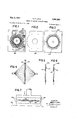
- FIG, 10 8 m k ⁇ w l I 1 N I 2/a F f" oooooc 32a V/j my 324 C) O O O C) C) Q, 2/? k 3/5 INVENTOR.
- Fig. l is a plan view of a circuit path depositing mask
- Fig. 2 is a plan view of a plate-like non-conducting element forming the base of a component structure
- Fig. 3 is a plan view of a circuit path depositing mask of a different kind
- Fig. 4 is a side elevational view of a component base impressed between two conducting path depositing masks disposed in the path of a pair of metal spraying nozzles;
- Fig. 5 is a side elevational view of a component after conducting paths have been deposited thereon;
- Fig. 6 is a view similar to Fig. 5 but shows the manner in which circuit paths have been embedded in the component base by application of pressure;
- Fig. 7 is a fragmentary view of a press having between the plates thereof a circuit element component
- Fig. 8 is an enlarged fragmentary sectional view of a component showing the nature of a transverse impulse conducting path formed therein;
- Fig. 9 is an enlarged fragmentary cross-sectional view through a component showing the manner in which transverse conducting paths may be plugged;
- Fig. 10 is a fragmentary cross-sectional View through atent an element prior to compression thereof, and shows in the transverse passage a forming pin;
- Fig. 11 is a fragmentary sectional view through a pair of pressed plates showing the condition of the component of Fig. 10 after application of pressure.
- circuit paths forming a part of the element be deposited on a receiving base, so that the path in eifect becomes a part of the base. It has been known heretofore to provide electrical circuits by painting, spraying or printing a metallic ink, paint or liquid composition on the surface of a non-conducting sheet, and in general, the method herein involved contemplates certain improvements on the methods heretofore used.
- the term deposited, as herein used, is to be taken, therefore, in its broad sense to embrace painting, printing, spraying or otherwise applying to a base component a current conducting coatingin the form of circuit paths.
- one specific practice of the method involves the application of a mask or template to opposite sides of a non-conducting component sheet and the formation of circuit paths upon such non-conducting component sheet by spraying against the opposite faces thereof a metal fog or mist produced by projecting molten metal from a nozzle under suitable fluid pressure.
- any more or less liquid conducting composition may be employed for depositing the circuit paths.
- a metallic ink can be employed and such deposits may be subsequently electro-plated with an appropriate material to form a deposit of substantial thickness and one having the desired strength and capacity.
- compositions consisting of a finely powdered metal with a quick drying resinous binder. Such compositions may be employed for spraying, painting or otherwise depositing the circuit paths. The latter compositions are particularly adapted for screen printing the circuit paths on to the dielectric base plates of the components. Circuit paths so deposited may be quickly dried by subjecting them to a temperature sufficiently high to volatilize the liquidifying constituent.
- the circuit paths may be deposited on the insulating base of the components by sputtering or vapor transfer of metal under a vacuum.
- the base plates are first conditioned by defining the portions on which the circuits are to be deposited by rendering such portions conductive and by the use of a mask, respectively, so that the metal will adhere only to the areas so conditioned.
- Fig. 1 a mask 300, having therein a plurality of slots 302, which represent a circuit pattern sought to be deposited on the face of a circuit component sheet.
- Fig. 3 shows a mask 304, which is generally similar to that shown in Fig. 1, but wherein the slots 306, which are representative of the circuit to be deposited, are of a different form.
- a relatively thin yielding sheet of non-conducting material 308 of any desired shape or dimensions may be used as the base of the component on which circuit paths are deposited in accordance with the method.
- the deposition of the circuit forming paint or composition is preferably accomplished by spraying the composition in the predetermined patterns, as gov- 3 erned by the masks 300 and 304.
- the component base 308 is positioned between a pair of masks, such as 300 and 304, the masks being of sufficient size to cover all of the working area of the component base and being slotted according to the predetermined pattern, which is to constitute the deposited circuit path on opposie faces of the component base.
- the metal or other liquid or semi-liquid conducting composition may be sprayed or otherwise deposited against opposite faces of the component base, as diagrammatically represented in Fig. 4 of the drawings.
- the deposited conducting circuit paths are disposed on the component base in relief, as indicated at 310 and 312 in Fig. 5 of the drawings.
- the circuit path be wholly within the plane of the component base and preferably flush with the facial surface thereof to avoid undue wear of the contacting surfaces.
- a satisfactory position of the circuit paths is shown in Fig. 6, wherein the paths 310 and 312 are flush with the face of the component base 308. This objective is achieved by selecting a compressible component base and pressing the circuit paths into the base by subjecting the components to pressure after the paths have been deposited thereon.
- a suitable component base is a partially cured phenol condensate sheet possessing the necessary yielding characteristic to permit the circuit paths to be pressed into the face of the base. Since the specific base material is of no consequence so long as it is a non-conductor of electricity and possesses a yielding quality, a choice of such materials is available to those skilled in the art.
- the component base may be a sheet or block of cellulose acetate or acrylic resin.
- the material employed may be either thermo-plastic or thermo-setting so long as the essential properties are present.
- a press of this type Will include as essential elements a pair of press plates 316, which may be provided with heating means, such as steam coils or electric resistance heaters 318. Higher pressures may be employed, but for successful operation at substantially higher pressures it may become necessary to use a mold to confine the lateral movement of the base material.
- the smooth, flush position of the path obtained by pressing the sprayed components is only one of the benefits fiowing from the exercise of this part of the method.
- the electrical circuit element may include a plurality of components which have on confronting faces circuit paths that occupy a common position, and which, therefore, lie in contact with each other when two or more components are placed in face-to-face relationship. It will be appreciated, therefore, that the pressing of a plurality of components will more effectively unite common conducting paths, so that such common paths will function as a single path.
- the transverse connections which electrically join intersecting circuit paths on opposite faces of a component, are formed by piercing the base of the component from face-to-face and by spraying or otherwise depositing an electrically conductive composition on the walls of the transverse passage. It is sometimes desirable that a transverse connector, whether interconnecting oppositely disposed circuit paths or not, be adapted to receive a connecting plug. Without exercising specific precaution to render the transverse connection pluggable, the passage leading from one face of a component to another may be partially or completely blocked by the conducting composition during the spraying operation. Such condition is particularly prevalent after subjecting the component to pressure. In Fig.
- FIG. 8 is shown a section of a component base 308, having deposited thereon oppositely disposed circuit paths 320 and 322.
- a transverse connecting passage has been formed in the base 308 by piercing the base in the zone of oppositely disposed circuit paths 320 and 322.
- the conducting material has been sprayed into the passage forming an interconnecting annulus 324 therein.
- the shape and position of the inner walls of the annulus 324 are normally beyond accurate control, and it frequently happens, particularly after the element has been compressed, that the transverse passage is completely obliterated, whereas the desired condition, as shown in Fig. 9, is one in which the walls of the annulus 324 remain substantially cylindrical for the ready reception of a conducting plug 326.
- the desired condition can best be brought about by inserting a forming element such as a plug into the passage prior to the pressing operation.
- a plug 328 may be inserted into the passage before the component is subjected to pressure, and as seen from Fig. 11 of the drawing, when a component so conditioned is placed between the plates 316 of the press 314 and subjected to pressure therebetween, the plug 328 will serve to form a connecting transverse passage having cylindrical walls 324, which are adapted to the plugging function referred to.
- Figs. 8 through 11 of the drawings The procedure shown in Figs. 8 through 11 of the drawings is, of course, simply for the purpose of suggesting the steps that may be used to achieve the purpose, and any suitable or feasible procedure may be resorted to, so long as a sustaining element is used in the through passage for molding and shaping the walls of the passage during the pressing operation. It is contemplated that the forming elements or plugs 328 be adapted for mechanical manipulation as, for example, by incorporating them into the base or head platen of the press 314.
- the method of forming an electric circuit carrying panel which comprises spraying a conductive material to form a predetermined circuit pattern including individual conductors on at least one surface of a semi-cured, deformable panel of thermo-setting dielectric material, and simultaneously applying heat and pressure to the panel and the circuit pattern thereon to embed the circuit pattern into flush relation with the dielectric surface and to harden and cure the panel.
- the method of forming an electric circuit carrying panel which comprises spraying a conductive material to form a predetermined circuit pattern including individual conductors on atleast one surface of a semi-cured, deformable panel of thermo-setting dielectric material, and
- the method of forming an electric circuit carrying panel which comprises spraying a conductive material to orm predetermined circuit patterns on each of the opposed surfaces of a semi-cured, deformable panel of thermo-setting dieletcric material, and simultaneously applying heat and pressure to such opposed surfaces to embed the circuit patterns into flush relation with the dielectric surfaces, and to harden and cure the panel.
- the method of making electricalcircuit elements which consists in depositing a circuit path of conductive material on the face of a partially cured phenol condensate base panel, subjecting said base panel and circuit path thereon, to a pressure of l000-2000 pounds per square inch of base panel to press the circuit path into the base panel, and subjecting said base panel to a temperature of BOO-350 F. while compressing the same to complete the curing of the base panel.
- the method of making electrical circuit elements which consists in depositing a circuit path of conductive material on the face of a partially cured panel of thermosetting material which will cure in a heat of 300-350 R, subjecting such panel and circuit path thereon to a pressure of 1000-2000 pounds per square inches of panel to press the circuit path into the base panel, and subjecting said base panel to a temperature of 300-350" F. while compressing the same to complete the curing of the base panel.
Landscapes
- Engineering & Computer Science (AREA)
- Manufacturing & Machinery (AREA)
- Microelectronics & Electronic Packaging (AREA)
- Manufacturing Of Printed Wiring (AREA)
Description
May 2, 1961 H. P. LUHN METHOD OF MAKING CIRCUIT PANELS Original Filed March 8, 1949 2 Sheets-Sheet 1 v N 3 0 W a m W$ 000IMQ m M ma m 5 M? 3 WM j w 0 T 0 Z M w M 6 a 0 .M0 q. W WM o M I! Q o w E1 7 N M 1 W \\\\\&\\M m w o G m %\M w H a May 2, 1961 H. P. LUHN 2,981,981
METHOD OF MAKING CIRCUIT PANELS Original Filed March 8, 1949 2 Sheets-Sheet 2 FIG.9
FIG, 10 8 m k\\ w l I 1 N I 2/a F f" oooooc 32a V/j my 324 C) O O O C) C) Q, 2/? k 3/5 INVENTOR.
HANS P. LUHN ATTORNEY.
2,981,981 7 METHOD OF MAKING CIRCUIT PANELS Hans P. Luhn, Armouk, N.Y., assignor to International Business Machines Corporation, New York, N.Y., a corporation of New York Original application Mar. 8, 1949, Ser. No. 80,266, now Patent No. 2,649,513, dated Aug. 18, 1953. Divided and this application Apr. 13, 1953, Ser. No. 348,352
7 Claims. (Cl. 18-59) This invention relates to a method of making circuit panels, this application being a division of Hans P. Luhn application, Serial No. 80,266, filed March 8, 1949, now Patent No. 2,649,513 issued August 18, 1953, for Distributor and Method for Making the Same.
It is an object of this invention to provide an improved method for making circuit panels that are formed by depositing current conducting paths on a dielectric supporting base, and in this regard certain improved procedures are contemplated herein.
In connection with the method described herein, it is an object to provide a distributor or other electrical circuit component of the deposited metal type which will present a smooth contact face for cooperation with a movablepart such as a wiper brush, whereby a good electrical contact is provided and the contacting parts subject to movement therebetween, as between a fixed con tact and a movable wiper, are protected against undue wear during their operation.
Furthermore, it is an important object of the invention to provide improved, durable, deposited, circuit paths on a supporting base, and particularly depositing the circuit paths in firmly bonded relation to their supporting base.
It is also an important object hereof to provide a circuit element of the type indicated wherein current conductors are disposed in a unitary supporting body, and the method disclosed herein contemplates the production of current conducting elements composed of a plurality of components disposed in spaced planes within a unitary supporting body.
Further objects and advantages of the invention will appear as the following detailed specification is read with reference to the drawings forming a part hereof and in which drawings:
Fig. l is a plan view of a circuit path depositing mask;
Fig. 2 is a plan view of a plate-like non-conducting element forming the base of a component structure;
Fig. 3 is a plan view of a circuit path depositing mask of a different kind;
Fig. 4 is a side elevational view of a component base impressed between two conducting path depositing masks disposed in the path of a pair of metal spraying nozzles;
Fig. 5 is a side elevational view of a component after conducting paths have been deposited thereon;
Fig. 6 is a view similar to Fig. 5 but shows the manner in which circuit paths have been embedded in the component base by application of pressure;
Fig. 7 is a fragmentary view of a press having between the plates thereof a circuit element component;
Fig. 8 is an enlarged fragmentary sectional view of a component showing the nature of a transverse impulse conducting path formed therein;
Fig. 9 is an enlarged fragmentary cross-sectional view through a component showing the manner in which transverse conducting paths may be plugged;
. Fig. 10 is a fragmentary cross-sectional View through atent an element prior to compression thereof, and shows in the transverse passage a forming pin; and
Fig. 11 is a fragmentary sectional view through a pair of pressed plates showing the condition of the component of Fig. 10 after application of pressure.
It is contemplated that all circuit paths forming a part of the element be deposited on a receiving base, so that the path in eifect becomes a part of the base. It has been known heretofore to provide electrical circuits by painting, spraying or printing a metallic ink, paint or liquid composition on the surface of a non-conducting sheet, and in general, the method herein involved contemplates certain improvements on the methods heretofore used. The term deposited, as herein used, is to be taken, therefore, in its broad sense to embrace painting, printing, spraying or otherwise applying to a base component a current conducting coatingin the form of circuit paths.
In brief, one specific practice of the method involves the application of a mask or template to opposite sides of a non-conducting component sheet and the formation of circuit paths upon such non-conducting component sheet by spraying against the opposite faces thereof a metal fog or mist produced by projecting molten metal from a nozzle under suitable fluid pressure.
Any more or less liquid conducting composition may be employed for depositing the circuit paths. For example, a metallic ink can be employed and such deposits may be subsequently electro-plated with an appropriate material to form a deposit of substantial thickness and one having the desired strength and capacity.
There is available a coating composition consisting of a finely powdered metal with a quick drying resinous binder. Such compositions may be employed for spraying, painting or otherwise depositing the circuit paths. The latter compositions are particularly adapted for screen printing the circuit paths on to the dielectric base plates of the components. Circuit paths so deposited may be quickly dried by subjecting them to a temperature sufficiently high to volatilize the liquidifying constituent.
The formation of parts of the circuits which are subject to mechanical wear are best formed by the spraying of metal because of the tough, wear-resisting quality of such sprayedsurfaces. However, less wear-resistent circuits may be traced on parts of the element that are not subject to mechanical Wear, and for such circuits metallic paints, inks and other conducting coating compositions may be employed with advantage.
Further, it is contemplated that the circuit paths may be deposited on the insulating base of the components by sputtering or vapor transfer of metal under a vacuum. For the purpose of such procedures, the base plates are first conditioned by defining the portions on which the circuits are to be deposited by rendering such portions conductive and by the use of a mask, respectively, so that the metal will adhere only to the areas so conditioned.
In Fig. 1 is illustrated a mask 300, having therein a plurality of slots 302, which represent a circuit pattern sought to be deposited on the face of a circuit component sheet. Fig. 3 shows a mask 304, which is generally similar to that shown in Fig. 1, but wherein the slots 306, which are representative of the circuit to be deposited, are of a different form. A relatively thin yielding sheet of non-conducting material 308 of any desired shape or dimensions may be used as the base of the component on which circuit paths are deposited in accordance with the method. The deposition of the circuit forming paint or composition is preferably accomplished by spraying the composition in the predetermined patterns, as gov- 3 erned by the masks 300 and 304. Accordingly, the component base 308 is positioned between a pair of masks, such as 300 and 304, the masks being of sufficient size to cover all of the working area of the component base and being slotted according to the predetermined pattern, which is to constitute the deposited circuit path on opposie faces of the component base. After assembly of the masks with the component base sheet, the metal or other liquid or semi-liquid conducting composition may be sprayed or otherwise deposited against opposite faces of the component base, as diagrammatically represented in Fig. 4 of the drawings.
After the spraying operation has been completed the deposited conducting circuit paths are disposed on the component base in relief, as indicated at 310 and 312 in Fig. 5 of the drawings. For certain purposes, particularly in connection with the use of a wiper brush or the like that has mechanical contact with and regular or intermittent movement in contact with such deposited part, it is desirable that the circuit path be wholly within the plane of the component base and preferably flush with the facial surface thereof to avoid undue wear of the contacting surfaces. A satisfactory position of the circuit paths is shown in Fig. 6, wherein the paths 310 and 312 are flush with the face of the component base 308. This objective is achieved by selecting a compressible component base and pressing the circuit paths into the base by subjecting the components to pressure after the paths have been deposited thereon. In a specific practice of this phase of the method, it has been found that a suitable component base is a partially cured phenol condensate sheet possessing the necessary yielding characteristic to permit the circuit paths to be pressed into the face of the base. Since the specific base material is of no consequence so long as it is a non-conductor of electricity and possesses a yielding quality, a choice of such materials is available to those skilled in the art. For
example, the component base may be a sheet or block of cellulose acetate or acrylic resin. The material employed may be either thermo-plastic or thermo-setting so long as the essential properties are present.
When a partially cured phenol condensate base is employed, it is appropriate to press the sprayed plate while applying heat to effect the further and complete curing thereof. Herein it is contemplated, therefore, that the components be compressed at a temperature of 300 to 350 F. and under a pressure of 1000 to 2000 pounds per square inch, as, for example, in a press 314, such as diagrammatically and partially illustrated in Fig. 7 of the drawings. A press of this type Will include as essential elements a pair of press plates 316, which may be provided with heating means, such as steam coils or electric resistance heaters 318. Higher pressures may be employed, but for successful operation at substantially higher pressures it may become necessary to use a mold to confine the lateral movement of the base material.
The smooth, flush position of the path obtained by pressing the sprayed components is only one of the benefits fiowing from the exercise of this part of the method. The electrical circuit element may include a plurality of components which have on confronting faces circuit paths that occupy a common position, and which, therefore, lie in contact with each other when two or more components are placed in face-to-face relationship. It will be appreciated, therefore, that the pressing of a plurality of components will more effectively unite common conducting paths, so that such common paths will function as a single path. When using a compressible component base material, as for example, semi-cured phenol condensate, pressing of a plurality of components in face-to-face contact under heat and pressure will result in the flowing together or fusing of the separate component base members into such intimate relation as to form a unitary structure, S ch structure beingin effect a single mnlti-circuit carrying body of homogenous character.
It has been pointed out hereinbefore that the transverse connections, which electrically join intersecting circuit paths on opposite faces of a component, are formed by piercing the base of the component from face-to-face and by spraying or otherwise depositing an electrically conductive composition on the walls of the transverse passage. It is sometimes desirable that a transverse connector, whether interconnecting oppositely disposed circuit paths or not, be adapted to receive a connecting plug. Without exercising specific precaution to render the transverse connection pluggable, the passage leading from one face of a component to another may be partially or completely blocked by the conducting composition during the spraying operation. Such condition is particularly prevalent after subjecting the component to pressure. In Fig. 8 is shown a section of a component base 308, having deposited thereon oppositely disposed circuit paths 320 and 322. Herein a transverse connecting passage has been formed in the base 308 by piercing the base in the zone of oppositely disposed circuit paths 320 and 322. Thereafter the conducting material has been sprayed into the passage forming an interconnecting annulus 324 therein. The shape and position of the inner walls of the annulus 324 are normally beyond accurate control, and it frequently happens, particularly after the element has been compressed, that the transverse passage is completely obliterated, whereas the desired condition, as shown in Fig. 9, is one in which the walls of the annulus 324 remain substantially cylindrical for the ready reception of a conducting plug 326.
The desired condition can best be brought about by inserting a forming element such as a plug into the passage prior to the pressing operation. Thus, a plug 328 may be inserted into the passage before the component is subjected to pressure, and as seen from Fig. 11 of the drawing, when a component so conditioned is placed between the plates 316 of the press 314 and subjected to pressure therebetween, the plug 328 will serve to form a connecting transverse passage having cylindrical walls 324, which are adapted to the plugging function referred to.
The procedure shown in Figs. 8 through 11 of the drawings is, of course, simply for the purpose of suggesting the steps that may be used to achieve the purpose, and any suitable or feasible procedure may be resorted to, so long as a sustaining element is used in the through passage for molding and shaping the walls of the passage during the pressing operation. It is contemplated that the forming elements or plugs 328 be adapted for mechanical manipulation as, for example, by incorporating them into the base or head platen of the press 314.
The practice of the invention in its several aspects has been shown and described herein in single embodiments merely for the purpose of rendering concise the explanation thereof. Certain modifications have been alluded to for the purpose of suggesting the broader aspects. It is intended, therefore, to be limited only as indicated by the scope of the following claims.
, I claim:
l. The method of forming an electric circuit carrying panel which comprises spraying a conductive material to form a predetermined circuit pattern including individual conductors on at least one surface of a semi-cured, deformable panel of thermo-setting dielectric material, and simultaneously applying heat and pressure to the panel and the circuit pattern thereon to embed the circuit pattern into flush relation with the dielectric surface and to harden and cure the panel. 7
2. The method of forming an electric circuit carrying panel which comprises spraying a conductive material to form a predetermined circuit pattern including individual conductors on atleast one surface of a semi-cured, deformable panel of thermo-setting dielectric material, and
simultaneously applying heat and pressure to the circuit pattern carrying surface andthe opposite surface of the panel to embed the circuit pattern into flush relation withlthe dielectric surface and to harden and cure the pane 3. The method of forming an electric circuit carrying panel which comprises spraying a conductive material to orm predetermined circuit patterns on each of the opposed surfaces of a semi-cured, deformable panel of thermo-setting dieletcric material, and simultaneously applying heat and pressure to such opposed surfaces to embed the circuit patterns into flush relation with the dielectric surfaces, and to harden and cure the panel.
4. The method of making electrical circuit elements, which consists in spraying a circuit path of conductive material on the face of a semi-cured, non-conducting, thermo-setting base component, subjecting such component and circuit path thereon to sufiicient pressure to press the path into the base component, and simultaneously applying heat to the component to complete the curing thereof.
5. The method of making electricalcircuit elements, which consists in depositing a circuit path of conductive material on the face of a partially cured phenol condensate base panel, subjecting said base panel and circuit path thereon, to a pressure of l000-2000 pounds per square inch of base panel to press the circuit path into the base panel, and subjecting said base panel to a temperature of BOO-350 F. while compressing the same to complete the curing of the base panel.
6. The method of making electrical circuit elements, which consists in depositing a circuit path of conductive material on the face of a partially cured panel of thermosetting material which will cure in a heat of 300-350 R, subjecting such panel and circuit path thereon to a pressure of 1000-2000 pounds per square inches of panel to press the circuit path into the base panel, and subjecting said base panel to a temperature of 300-350" F. while compressing the same to complete the curing of the base panel.
7. The method of forming an electrical circuit pattern, which consists in forming a plurality of spaced individual conductors on at least one surface of a semi-cured, deformable panel of thermo-setting dielectric material, and applying heat and simultaneous pressure to the panel and the conductors thereon to embed the conductors into flush relation with the dielectric surface and to harden and cure the panel.
References Cited in the file of this patent UNITED STATES PATENTS 1,987,969 Parkin June 15, 1935 2,064,971 Edison Dec. 22, 1936 2,289,339 Brennan July 14, 1942 2,626,206 Adler et a1. Jan. 20, 1953 FOREIGN PATENTS 570,877 Great Britain Aug. 23, 1944
Priority Applications (1)
| Application Number | Priority Date | Filing Date | Title |
|---|---|---|---|
| US348352A US2981981A (en) | 1949-03-08 | 1953-04-13 | Method of making circuit panels |
Applications Claiming Priority (2)
| Application Number | Priority Date | Filing Date | Title |
|---|---|---|---|
| US80266A US2649513A (en) | 1949-03-08 | 1949-03-08 | Distributor and method for making the same |
| US348352A US2981981A (en) | 1949-03-08 | 1953-04-13 | Method of making circuit panels |
Publications (1)
| Publication Number | Publication Date |
|---|---|
| US2981981A true US2981981A (en) | 1961-05-02 |
Family
ID=26763296
Family Applications (1)
| Application Number | Title | Priority Date | Filing Date |
|---|---|---|---|
| US348352A Expired - Lifetime US2981981A (en) | 1949-03-08 | 1953-04-13 | Method of making circuit panels |
Country Status (1)
| Country | Link |
|---|---|
| US (1) | US2981981A (en) |
Cited By (5)
| Publication number | Priority date | Publication date | Assignee | Title |
|---|---|---|---|---|
| US3264385A (en) * | 1963-01-14 | 1966-08-02 | American Scient Corp | Method of casting a printed pattern on a plastic sheet |
| US3277418A (en) * | 1963-04-23 | 1966-10-04 | Ace Electronics Associates Inc | Molded conductive plastic resistors and methods of making same |
| US3458930A (en) * | 1967-12-07 | 1969-08-05 | Zenith Radio Corp | Leadless inverted device forming process |
| US3520054A (en) * | 1967-11-13 | 1970-07-14 | Mitronics Inc | Method of making multilevel metallized ceramic bodies for semiconductor packages |
| US5145691A (en) * | 1990-07-18 | 1992-09-08 | Nippon Cmk Corp. | Apparatus for packing filler into through-holes or the like in a printed circuit board |
Citations (5)
| Publication number | Priority date | Publication date | Assignee | Title |
|---|---|---|---|---|
| US1987969A (en) * | 1927-05-13 | 1935-01-15 | Rca Corp | Process for the manufacture of high resistances |
| US2064971A (en) * | 1932-01-13 | 1936-12-22 | Edison Inc Thomas A | Heating unit and the production thereof |
| US2289339A (en) * | 1938-08-20 | 1942-07-14 | Joseph B Brennan | Method for making electric devices |
| GB570877A (en) * | 1943-08-30 | 1945-07-26 | John Adolph Sargrove | Improvements in and relating to methods of manufacturing electrical apparatus such as electronic communication apparatus and the like |
| US2626206A (en) * | 1951-09-10 | 1953-01-20 | Etched Products Corp | Method of making circuit panels |
-
1953
- 1953-04-13 US US348352A patent/US2981981A/en not_active Expired - Lifetime
Patent Citations (5)
| Publication number | Priority date | Publication date | Assignee | Title |
|---|---|---|---|---|
| US1987969A (en) * | 1927-05-13 | 1935-01-15 | Rca Corp | Process for the manufacture of high resistances |
| US2064971A (en) * | 1932-01-13 | 1936-12-22 | Edison Inc Thomas A | Heating unit and the production thereof |
| US2289339A (en) * | 1938-08-20 | 1942-07-14 | Joseph B Brennan | Method for making electric devices |
| GB570877A (en) * | 1943-08-30 | 1945-07-26 | John Adolph Sargrove | Improvements in and relating to methods of manufacturing electrical apparatus such as electronic communication apparatus and the like |
| US2626206A (en) * | 1951-09-10 | 1953-01-20 | Etched Products Corp | Method of making circuit panels |
Cited By (5)
| Publication number | Priority date | Publication date | Assignee | Title |
|---|---|---|---|---|
| US3264385A (en) * | 1963-01-14 | 1966-08-02 | American Scient Corp | Method of casting a printed pattern on a plastic sheet |
| US3277418A (en) * | 1963-04-23 | 1966-10-04 | Ace Electronics Associates Inc | Molded conductive plastic resistors and methods of making same |
| US3520054A (en) * | 1967-11-13 | 1970-07-14 | Mitronics Inc | Method of making multilevel metallized ceramic bodies for semiconductor packages |
| US3458930A (en) * | 1967-12-07 | 1969-08-05 | Zenith Radio Corp | Leadless inverted device forming process |
| US5145691A (en) * | 1990-07-18 | 1992-09-08 | Nippon Cmk Corp. | Apparatus for packing filler into through-holes or the like in a printed circuit board |
Similar Documents
| Publication | Publication Date | Title |
|---|---|---|
| US2649513A (en) | Distributor and method for making the same | |
| US2757443A (en) | Method of making printed circuits | |
| US2695351A (en) | Electric circuit components and methods of preparing the same | |
| US2943956A (en) | Printed electrical circuits and method of making the same | |
| US2721153A (en) | Production of conducting layers upon electrical resistors | |
| DE9107710U1 (en) | Three-dimensional circuit substrate | |
| US2981981A (en) | Method of making circuit panels | |
| US2721152A (en) | Production of electrical elements | |
| US5061438A (en) | Method of making a printed circuit board | |
| DE2712598A1 (en) | METHOD OF CREATING AT LEAST ONE ELECTRICALLY CONDUCTIVE PATH THROUGH A NON-CONDUCTIVE PART | |
| US1985166A (en) | Method of making electric resistance | |
| US3107190A (en) | Method of dielectrically embossing a metallic element to a thermoplastic | |
| US2679473A (en) | Method of preparing molds to produce crackle and other surface finishes on molded plastic articles | |
| US2984697A (en) | Pre-wired circuit panel | |
| US5094811A (en) | Method of making a printed circuit board | |
| EP0138673A2 (en) | Method of making a printed circuit board | |
| DE69810575T2 (en) | Electroluminescent element | |
| US3303078A (en) | Method of making electrical components | |
| US2087311A (en) | Composite article and method of making composite articles | |
| US2148453A (en) | Resistance | |
| US4743464A (en) | Process for manufacturing capacitive keyboards and new keyboards obtained by this process | |
| US3307111A (en) | Molded composition resistor with parallel leads | |
| US2823286A (en) | Contacts for electrical circuits and methods for making same | |
| DE1416437B2 (en) | Carrier plate for microminiaturized switching elements and process for their production | |
| US3315309A (en) | Apparatus for molding composition resistors |