US2956912A - Lead sulphide semi-conductive bodies and method of making same - Google Patents
Lead sulphide semi-conductive bodies and method of making same Download PDFInfo
- Publication number
- US2956912A US2956912A US580912A US58091256A US2956912A US 2956912 A US2956912 A US 2956912A US 580912 A US580912 A US 580912A US 58091256 A US58091256 A US 58091256A US 2956912 A US2956912 A US 2956912A
- Authority
- US
- United States
- Prior art keywords
- lead
- layer
- lead sulphide
- sulphide
- semi
- Prior art date
- Legal status (The legal status is an assumption and is not a legal conclusion. Google has not performed a legal analysis and makes no representation as to the accuracy of the status listed.)
- Expired - Lifetime
Links
- XCAUINMIESBTBL-UHFFFAOYSA-N lead(ii) sulfide Chemical compound [Pb]=S XCAUINMIESBTBL-UHFFFAOYSA-N 0.000 title claims description 63
- 238000004519 manufacturing process Methods 0.000 title description 5
- 238000001556 precipitation Methods 0.000 claims description 9
- 238000000034 method Methods 0.000 description 19
- UMGDCJDMYOKAJW-UHFFFAOYSA-N thiourea Chemical compound NC(N)=S UMGDCJDMYOKAJW-UHFFFAOYSA-N 0.000 description 14
- OAKJQQAXSVQMHS-UHFFFAOYSA-N Hydrazine Chemical compound NN OAKJQQAXSVQMHS-UHFFFAOYSA-N 0.000 description 10
- XSQUKJJJFZCRTK-UHFFFAOYSA-N Urea Natural products NC(N)=O XSQUKJJJFZCRTK-UHFFFAOYSA-N 0.000 description 7
- 229940046892 lead acetate Drugs 0.000 description 7
- 230000001376 precipitating effect Effects 0.000 description 7
- HEMHJVSKTPXQMS-UHFFFAOYSA-M Sodium hydroxide Chemical compound [OH-].[Na+] HEMHJVSKTPXQMS-UHFFFAOYSA-M 0.000 description 6
- 229910001854 alkali hydroxide Inorganic materials 0.000 description 6
- 150000008044 alkali metal hydroxides Chemical class 0.000 description 6
- 238000010438 heat treatment Methods 0.000 description 6
- 239000011521 glass Substances 0.000 description 5
- 229910052738 indium Inorganic materials 0.000 description 5
- 239000003513 alkali Substances 0.000 description 4
- 229910052733 gallium Inorganic materials 0.000 description 4
- 229910052782 aluminium Inorganic materials 0.000 description 3
- 229910052787 antimony Inorganic materials 0.000 description 3
- 229910052785 arsenic Inorganic materials 0.000 description 3
- 229910052797 bismuth Inorganic materials 0.000 description 3
- 230000008021 deposition Effects 0.000 description 3
- APFVFJFRJDLVQX-UHFFFAOYSA-N indium atom Chemical compound [In] APFVFJFRJDLVQX-UHFFFAOYSA-N 0.000 description 3
- 229910052751 metal Inorganic materials 0.000 description 3
- 239000002184 metal Substances 0.000 description 3
- 239000000203 mixture Substances 0.000 description 3
- 229910052750 molybdenum Inorganic materials 0.000 description 3
- 239000000126 substance Substances 0.000 description 3
- 229910052719 titanium Inorganic materials 0.000 description 3
- 239000010936 titanium Substances 0.000 description 3
- 229910052721 tungsten Inorganic materials 0.000 description 3
- 229910052720 vanadium Inorganic materials 0.000 description 3
- NWZSZGALRFJKBT-KNIFDHDWSA-N (2s)-2,6-diaminohexanoic acid;(2s)-2-hydroxybutanedioic acid Chemical compound OC(=O)[C@@H](O)CC(O)=O.NCCCC[C@H](N)C(O)=O NWZSZGALRFJKBT-KNIFDHDWSA-N 0.000 description 2
- OKTJSMMVPCPJKN-UHFFFAOYSA-N Carbon Chemical compound [C] OKTJSMMVPCPJKN-UHFFFAOYSA-N 0.000 description 2
- GYHNNYVSQQEPJS-UHFFFAOYSA-N Gallium Chemical compound [Ga] GYHNNYVSQQEPJS-UHFFFAOYSA-N 0.000 description 2
- ZOKXTWBITQBERF-UHFFFAOYSA-N Molybdenum Chemical compound [Mo] ZOKXTWBITQBERF-UHFFFAOYSA-N 0.000 description 2
- RTAQQCXQSZGOHL-UHFFFAOYSA-N Titanium Chemical compound [Ti] RTAQQCXQSZGOHL-UHFFFAOYSA-N 0.000 description 2
- 238000010521 absorption reaction Methods 0.000 description 2
- XAGFODPZIPBFFR-UHFFFAOYSA-N aluminium Chemical compound [Al] XAGFODPZIPBFFR-UHFFFAOYSA-N 0.000 description 2
- RQNWIZPPADIBDY-UHFFFAOYSA-N arsenic atom Chemical compound [As] RQNWIZPPADIBDY-UHFFFAOYSA-N 0.000 description 2
- JCXGWMGPZLAOME-UHFFFAOYSA-N bismuth atom Chemical compound [Bi] JCXGWMGPZLAOME-UHFFFAOYSA-N 0.000 description 2
- 229910002804 graphite Inorganic materials 0.000 description 2
- 239000010439 graphite Substances 0.000 description 2
- IKDUDTNKRLTJSI-UHFFFAOYSA-N hydrazine monohydrate Substances O.NN IKDUDTNKRLTJSI-UHFFFAOYSA-N 0.000 description 2
- 239000011733 molybdenum Substances 0.000 description 2
- 239000000725 suspension Substances 0.000 description 2
- WFKWXMTUELFFGS-UHFFFAOYSA-N tungsten Chemical compound [W] WFKWXMTUELFFGS-UHFFFAOYSA-N 0.000 description 2
- 239000010937 tungsten Substances 0.000 description 2
- LEONUFNNVUYDNQ-UHFFFAOYSA-N vanadium atom Chemical compound [V] LEONUFNNVUYDNQ-UHFFFAOYSA-N 0.000 description 2
- 241000206607 Porphyra umbilicalis Species 0.000 description 1
- WATWJIUSRGPENY-UHFFFAOYSA-N antimony atom Chemical compound [Sb] WATWJIUSRGPENY-UHFFFAOYSA-N 0.000 description 1
- 229910052793 cadmium Inorganic materials 0.000 description 1
- 239000003795 chemical substances by application Substances 0.000 description 1
- 229910052802 copper Inorganic materials 0.000 description 1
- 230000000694 effects Effects 0.000 description 1
- 229910052737 gold Inorganic materials 0.000 description 1
- 229910052742 iron Inorganic materials 0.000 description 1
- 229910052745 lead Inorganic materials 0.000 description 1
- 238000005259 measurement Methods 0.000 description 1
- 229910052759 nickel Inorganic materials 0.000 description 1
- 230000001590 oxidative effect Effects 0.000 description 1
- 230000005855 radiation Effects 0.000 description 1
- 239000011541 reaction mixture Substances 0.000 description 1
- 229910052709 silver Inorganic materials 0.000 description 1
- 230000007704 transition Effects 0.000 description 1
- 229910052725 zinc Inorganic materials 0.000 description 1
Images
Classifications
-
- H—ELECTRICITY
- H01—ELECTRIC ELEMENTS
- H01L—SEMICONDUCTOR DEVICES NOT COVERED BY CLASS H10
- H01L31/00—Semiconductor devices sensitive to infrared radiation, light, electromagnetic radiation of shorter wavelength or corpuscular radiation and specially adapted either for the conversion of the energy of such radiation into electrical energy or for the control of electrical energy by such radiation; Processes or apparatus specially adapted for the manufacture or treatment thereof or of parts thereof; Details thereof
-
- H—ELECTRICITY
- H01—ELECTRIC ELEMENTS
- H01B—CABLES; CONDUCTORS; INSULATORS; SELECTION OF MATERIALS FOR THEIR CONDUCTIVE, INSULATING OR DIELECTRIC PROPERTIES
- H01B1/00—Conductors or conductive bodies characterised by the conductive materials; Selection of materials as conductors
-
- H—ELECTRICITY
- H01—ELECTRIC ELEMENTS
- H01L—SEMICONDUCTOR DEVICES NOT COVERED BY CLASS H10
- H01L21/00—Processes or apparatus adapted for the manufacture or treatment of semiconductor or solid state devices or of parts thereof
-
- H—ELECTRICITY
- H01—ELECTRIC ELEMENTS
- H01L—SEMICONDUCTOR DEVICES NOT COVERED BY CLASS H10
- H01L21/00—Processes or apparatus adapted for the manufacture or treatment of semiconductor or solid state devices or of parts thereof
- H01L21/02—Manufacture or treatment of semiconductor devices or of parts thereof
- H01L21/04—Manufacture or treatment of semiconductor devices or of parts thereof the devices having at least one potential-jump barrier or surface barrier, e.g. PN junction, depletion layer or carrier concentration layer
- H01L21/34—Manufacture or treatment of semiconductor devices or of parts thereof the devices having at least one potential-jump barrier or surface barrier, e.g. PN junction, depletion layer or carrier concentration layer the devices having semiconductor bodies not provided for in groups H01L21/0405, H01L21/0445, H01L21/06, H01L21/16 and H01L21/18 with or without impurities, e.g. doping materials
- H01L21/46—Treatment of semiconductor bodies using processes or apparatus not provided for in groups H01L21/428
- H01L21/479—Application of electric currents or fields, e.g. for electroforming
-
- H—ELECTRICITY
- H01—ELECTRIC ELEMENTS
- H01L—SEMICONDUCTOR DEVICES NOT COVERED BY CLASS H10
- H01L29/00—Semiconductor devices adapted for rectifying, amplifying, oscillating or switching, or capacitors or resistors with at least one potential-jump barrier or surface barrier, e.g. PN junction depletion layer or carrier concentration layer; Details of semiconductor bodies or of electrodes thereof ; Multistep manufacturing processes therefor
- H01L29/02—Semiconductor bodies ; Multistep manufacturing processes therefor
- H01L29/12—Semiconductor bodies ; Multistep manufacturing processes therefor characterised by the materials of which they are formed
- H01L29/24—Semiconductor bodies ; Multistep manufacturing processes therefor characterised by the materials of which they are formed including, apart from doping materials or other impurities, only semiconductor materials not provided for in groups H01L29/16, H01L29/18, H01L29/20, H01L29/22
-
- H—ELECTRICITY
- H01—ELECTRIC ELEMENTS
- H01L—SEMICONDUCTOR DEVICES NOT COVERED BY CLASS H10
- H01L31/00—Semiconductor devices sensitive to infrared radiation, light, electromagnetic radiation of shorter wavelength or corpuscular radiation and specially adapted either for the conversion of the energy of such radiation into electrical energy or for the control of electrical energy by such radiation; Processes or apparatus specially adapted for the manufacture or treatment thereof or of parts thereof; Details thereof
- H01L31/08—Semiconductor devices sensitive to infrared radiation, light, electromagnetic radiation of shorter wavelength or corpuscular radiation and specially adapted either for the conversion of the energy of such radiation into electrical energy or for the control of electrical energy by such radiation; Processes or apparatus specially adapted for the manufacture or treatment thereof or of parts thereof; Details thereof in which radiation controls flow of current through the device, e.g. photoresistors
-
- H—ELECTRICITY
- H01—ELECTRIC ELEMENTS
- H01L—SEMICONDUCTOR DEVICES NOT COVERED BY CLASS H10
- H01L31/00—Semiconductor devices sensitive to infrared radiation, light, electromagnetic radiation of shorter wavelength or corpuscular radiation and specially adapted either for the conversion of the energy of such radiation into electrical energy or for the control of electrical energy by such radiation; Processes or apparatus specially adapted for the manufacture or treatment thereof or of parts thereof; Details thereof
- H01L31/18—Processes or apparatus specially adapted for the manufacture or treatment of these devices or of parts thereof
Description
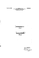
Oct. 18, 1960 F. A. KROGER ET AL 2,956,912 LEAD SULPHIDE SEMI-CONDUCTIVE BODIES AND METHOD OF MAKING SAME Filed April- 26, 1956 FIG.1
INVENTO R FERDINAND ANNE KROGER JAN BLOEM AGENT LEAD SULPHIDE SEMi-CQNDUCTIVE BODIES AND METHQD 6F MAKING SAME Ferdinand Anne Kroger and Jan Bloem, Eindho en, Netherlands, assigncrs, by mesne assignments, to North American Philips Company, Inc, New York, N.Y., a corporation of Delaware Filed Apr. 26, 1956,8er. No. 586,912 Claims priority, application Netherlands May 4, 1955 7 Claims. (Cl. 148-15) The invention relates to the production of semi-conductive devices, more uarticularlv photo-sensitive devices, by the precipitation of lead sulphide layers on a support.
It is well known that continuous lead sulphide layers having good adherence can be precipitated from a lead acetate solution in the presence of thio-urea and alkalihydroxide. Usually layers of p-tvne conductivity are produced by this method. It is thought possible that the absorption of alkali in the lead sulphide is significant in this process.
It is also possible for the alkali hydroxide to be replaced partly or even entirely by hydrazine so that layers are produced of a lesser p-type conductivity or even of n-type conductivity.
The lead sulphide layers produced by the said methods on usual support macterials, such as, for example, glass, always assume p-type conductivity when exposed to air. By heating the layers produced in air to temperatures between 70 C. and 120 C. for a period of, for example, 20 hours, the resistance of the layers becomes more stable and increases and consequently their photo-conductivity is improved.
In arriving at the invention, it was found experimentally that, when lead sulphide is precipitated on a support which has been previously provided with a laver consisting of one or more electropositive elements, said elements may influence the properties of the lead sulphide.
According to the invention, when producing semi-conductive devices, more particularly photo-sensitive devices, by the precipitation of lead sulphide on a supuort'from a solution of lead acetate in the presence of thio-urea and alkali hydroxide and/or hydrazine, the said support is at least in part previously provided with a layer consisting of one or more electro-positive elements, which during the precipitation of the lead sulphide are dissolved atso low a rate of speed that the process of dissolving is effected at least in part during the deposition of the lead sulphide layer. When the thickness of the said layer is so chosen that it does not completely dissolve during the precipitation of the lead sulphide, the remaining part may be used as acontact.
By dissolving the elements previously provided on the support, a reducing environment is produced at this point, so that lead sulphide containing a proportion of lead exceeding the exact .stoichiometric composition is deposited, which has a certain content of the said elements. Consequently, the conductivity properties are shifted in the direction of n-type conductivity.
When the lead sulphide layers thus produced are stored or heated in air, it was found that the elements from the dissolved layer which have been partly absorbed in the lead sulphide lattice have difierent effects according to their valency.
The layers produced with the use of monovalent elements, such as, for example, Cu, Ag, Au, after being heated in an oxidizing atmosphere to temperatures between 70" C. and 120 C., assume p-type conductivity and are stabilized against reduction. The use of bivalent elenited States Patent ments, such as, for example, Pb, Zn, Cd, Fe, Ni, Co, under the same conditions also results in the production of layers of p-type conductivity.
However, when the intermediate layer is produced from elements having a valency 3 or more, such as for example, A1, Ga, In, As, Sb, Bi, Ti, V, Mo, W, and when the lead sulphide is precipitated from a reaction mixture containing no alkali, the conductivity of the layers remains of the n-type after storing and heating in air. The same holds for lead sulphide layers precipitated in the presence of alkali, provided that this result is not cancelled by the absorption of alkali in the lead sulphide.
The support may be coated partly only with a layer of the said elements or in part with a monovalent or bivalent element and in part with an element of higher valency. ,This ensures that part of the lead sulphide exhibits conductivity properties which are difierent from those in another part. :More particularly, in this manner lead sulphide layers can be produced having portions of opposite conductivity types and a sharp p-n transition.
As will be seen from the preceding, the invention offers interesting possibilities in the production of semi-conductive devices, more particularly of photo-resistances and photo-electric cells. The precipitation of the lead sulphide layers in the examples described hereinafter can be carried out according to two difierent methods viz.:
(l) 6 cos. of a solution of 20 gms. of thio-urea per litre, 3 cos. of a solution of 400 gms. of lead acetate per litre and 0.7 cc. of a 50% hydrazine hydrate solution are stirred together for 5 minutes. A support is arranged in this mixture and 2 cos. of a solution of 666 gms. of NaOH per litre is added. After about 1 minute, again 0.8 cc. of this NaOH solution is added. After about 10 minutes an even lead sulphide layer has settled at room temperature.
(2) Equal parts of solutions containing 50 gms. of thio-urea per litre, 400 gms. of lead acetate per litre and 50% hydrazine hydrate, respectively, are mixed at room temperature. A support is arranged in the mixture, Which is stirred and subsequently is heated to 100 C. After a period of from 5 to 10 minutes an even lead sulphide layer is deposited on the support.
The concentrations of the solutions used in carrying out the above-mentioned methods may be varied within wide limits.
Example I As a support use is made of a glass plate one half of the surface of which has been provided previously, for
example by deposition from vapour, with a layer consisting of Al, Sb, In or Ga. Using the first of the two methods described 'her'einbefore, a lead-sulphide layer is precipitated on the support, the metal layers previously provided being dissolved. The lead-sulphide deposited on the metal has n-type conductivity and the lead-sulphide deposited on the glass has p-type conductivity. On both sides of the boundary provision is made of contacts, which are spaced away from each other by a distance of 5 mms. and extend throughout the entire width of the carrier, with the use of a graphite suspension. The Width of the leadsulphide layer between the contacts is 30 mms.
The following measurements have been taken on the device produced:
(1) l=resistance between the contacts, measured in the dark.
3 (3) E=photo-E.M.F. Both the E and the i are measured while the device is exposed to radiation having an intensity of 0.1 w./ sq. cm. (=10 quanta/ sec./ sq. cm.).
In the newly produced layer l=5.10 ohms,
and E=80 mv.
After heating for 20 hours at 100 C. in air, l= ohms,
and E=70 mv. After heating in air for 20 hours at 100 C., l=10 ohms,
and E=140 mv.
Example Ill About one half of a glass plate is coated with Ag and the remainder with Sb. Between the two metal layers a strip of about 1 mm. is kept clear.
With the use of the first method a lead-sulphide layer is deposited. Furthermore the same process. is used as described in Example I. In the newly produced layer, l=10 ohms,
and E=50 mv.
When the lead-sulphide is precipitated with the use of the second method, l=5.10 ohms,
and E: 85 mv.
Example IV If one half of a glass plate is coated with Ag and the other half with In, while proceeding otherwise entirely as is described in Example III, of the newly produced layer obtained by the first method, l=3.10 ohms,
and E=30 mv., and of the layer produced by the second method, l=7.10 ohms,
Example V In Fig. 1, reference numeral 1 designates a support provided with an indium layer 2. On this layer a leadsulphide layer 3 is deposited by the second of the two methods described hereinbefore, the indium layer being dissolved, as is shown in Fig. 2. The lead-sulphide layer 3, which exhibits n-type conductivity, is partly coated with a lead-sulphide layer 4 which, as usual, exhibits p-type conductivity. Finally, the two layers 3 and 4 are provided, by means of a graphite suspension, with contacts 5 and 6 respectively. In this arrangement, the lead-sulphide is photosensitive throughout the whole width between the contacts.
When the lead-sulphide layers 4 and 3 are deposited by the first and second of the two above-mentioned methods respectively, l=5.10 ohms,
and E= mv. After heating for 20 hours at C., l=4.l0 ohms,
and E=40 mv.
When the lead-sulphide layers 3 and 4 are both produced by the second method of deposition, l=3.10 ohms,
E=79 mv. and, after heating for 20 hours at 100 G, 1:10 ohms,
and E: 10 mv.
' In the manner described hereinbefore, lead-sulphide layers of difierent conductivity and/or different conductivity types and, if required, a number of successive superposed layers may be combined.
What is claimed is:
1. A lead sulphide semi-conductive body having n-type conductivity comprising a support having a surface portion containing any one of the electropositive elements aluminum, gallium, indium, arsenic, antimony, bismuth, titanium, vanadium, molybdenum, and tungsten whose valency exceeds 2, and on said surface portion a layer of lead sulphide produced by precipitation from a solution.
2. A lead sulphide semi-conductive body comprising a support having a surface portion containing an electropositive element whose valency exceeds 2, and an adjacent portion free of said element, and a lead sulphide layer on said surface and adjacent portions and produced by precipitation from a solution, said lead sulphide layer portion on said element-covered surface portion possessing n-type conductivity, said lead sulphide layer portion on said adjacent surface portion possessing p-type conductivity.
3. A body as set forth in claim 2 wherein said adjacent portion contains an electropositive element whose valency is below +3.
4. A lead sulphide semi-conductive body comprising a support having a surface portion containing an electropositive element whose valency exceeds 2, a first lead sulphide layer on said surface portion and produced by precipitation from a solution, and a second lead sulphide layer on said first layer, said first and second lead sulphide layers being of opposite type conductivity thus establishing a p-n junction between the layers.
5. A method of producing an n-type lead sulphide semiconductive body, which comprises slowly precipitating onto a support having a layer containing an electropositive element whose valency exceeds 2, a lead sulphide layer froma solution of lead acetate in the presence of thiourea and a substance selected from the group consisting of alkali hydroxide and hydrazine at which the precipitating lead sulphide layer dissolves all of the element layer and thus absorbs all of the elements atoms, and thereafter applying spaced contacts to the lead sulphide layer.
-6. A method of producing a lead sulphide semi-conductive body, which comprises slowly precipitating onto a support having a layer containing an electropositive element whose valency exceeds 2, a first lead sulphide layer from a solution of lead acetate in the presence of thiourea and a substance selected from the group consisting of alkali hydroxide and hydrazine at whichthe precipitating lead sulphide layer dissolves part of the element layer and thus absorbs some of the elements atoms, and thereafter precipitating by the same process a second layer of lead sulphide on the first formed layer of lead sulphide whereby the first and second layers exhibit opposite type conductivities.
7. A method of producing a lead sulphide semi-conductive body, which comprises slowly precipitating onto a support having a layer containing an electropositive ele- 15 2,809,132
ment selected from the group consisting of aluminum, gallium, arsenic, bismuth, titanium, vanadium, molybdenum, and tungsten, a lead sulphide layer from a solution of lead acetate in the presence of thiourea and a substance selected from the group consisting of alkali hydroxide and hydrazine at which the precipitating lead sulphide layer dissolves part of the element layer and thus absorbs some of the elements atoms.
References Cited in the file of this patent UNITED STATES PATENTS 1,919,988 Rupp July 25, 1933 1,998,334 Rupp Apr. 16, 1935 Bloern Oct. 8, 1957
Claims (1)
- 2. A LEAD SULPHIDE SEMI-CONDUCTIVE BODY COMPRISING A SUPPORT HAVING A SURFACE PORTION CONTAINING AN ELECTROPOSITIVE ELEMENT WHOSE VALENCY EXCEEDS 2, AND AN ADJACENT PORTION FREE OF SAID ELEMENT, AND A LEAD SULPHIDE LAYER ON SAID SURFACE AND ADJACENT PORTIONS AND PRODUCED BY PRECIPITATION FROM A SOLUTION, SAID LEAD SULPHIDE LAYER PORTION ON SAID ELEMENT-COVERED SURFACE PORTION POSSESSING N-TYPE CONDUCTIVITY, SAID LEAD SULPHIDE LAYER PORTION ON SAID ADJACENT SURFACE PORTION POSSESSING P-TYPE CONDUCTIVITY.
Applications Claiming Priority (2)
| Application Number | Priority Date | Filing Date | Title |
|---|---|---|---|
| NL1046193X | 1955-05-04 | ||
| NL341578X | 1955-05-04 |
Publications (1)
| Publication Number | Publication Date |
|---|---|
| US2956912A true US2956912A (en) | 1960-10-18 |
Family
ID=74667961
Family Applications (1)
| Application Number | Title | Priority Date | Filing Date |
|---|---|---|---|
| US580912A Expired - Lifetime US2956912A (en) | 1955-05-04 | 1956-04-26 | Lead sulphide semi-conductive bodies and method of making same |
Country Status (7)
| Country | Link |
|---|---|
| US (1) | US2956912A (en) |
| JP (1) | JPS319535B1 (en) |
| CH (1) | CH341578A (en) |
| DE (1) | DE1046193B (en) |
| FR (1) | FR1148323A (en) |
| GB (1) | GB841254A (en) |
| NL (2) | NL94394C (en) |
Cited By (3)
| Publication number | Priority date | Publication date | Assignee | Title |
|---|---|---|---|---|
| US3160800A (en) * | 1961-10-27 | 1964-12-08 | Westinghouse Electric Corp | High power semiconductor switch |
| US3160539A (en) * | 1958-09-08 | 1964-12-08 | Trw Semiconductors Inc | Surface treatment of silicon |
| US3366518A (en) * | 1964-07-01 | 1968-01-30 | Ibm | High sensitivity diodes |
Citations (3)
| Publication number | Priority date | Publication date | Assignee | Title |
|---|---|---|---|---|
| US1919988A (en) * | 1933-07-25 | Rectifier | ||
| US1998334A (en) * | 1931-08-13 | 1935-04-16 | Gen Electric | Electric radiation indicator |
| US2809132A (en) * | 1955-05-03 | 1957-10-08 | Philips Corp | Method of coating a support with a lead sulphide layer |
Family Cites Families (2)
| Publication number | Priority date | Publication date | Assignee | Title |
|---|---|---|---|---|
| DE617071C (en) * | 1931-09-11 | 1935-08-12 | Aeg | Process and device for the production of selenium cells |
| DE820318C (en) * | 1948-10-02 | 1951-11-08 | Siemens & Halske A G | Selenium bodies, especially for dry rectifiers, photo elements and light-sensitive resistance cells |
-
0
- NL NL197009D patent/NL197009A/xx unknown
- NL NL94394D patent/NL94394C/xx active
-
1956
- 1956-04-26 US US580912A patent/US2956912A/en not_active Expired - Lifetime
- 1956-04-30 DE DEN12185A patent/DE1046193B/en active Pending
- 1956-05-01 GB GB13381/56A patent/GB841254A/en not_active Expired
- 1956-05-02 FR FR1148323D patent/FR1148323A/en not_active Expired
- 1956-05-02 CH CH341578D patent/CH341578A/en unknown
- 1956-11-07 JP JP1153156A patent/JPS319535B1/ja active Pending
Patent Citations (3)
| Publication number | Priority date | Publication date | Assignee | Title |
|---|---|---|---|---|
| US1919988A (en) * | 1933-07-25 | Rectifier | ||
| US1998334A (en) * | 1931-08-13 | 1935-04-16 | Gen Electric | Electric radiation indicator |
| US2809132A (en) * | 1955-05-03 | 1957-10-08 | Philips Corp | Method of coating a support with a lead sulphide layer |
Cited By (3)
| Publication number | Priority date | Publication date | Assignee | Title |
|---|---|---|---|---|
| US3160539A (en) * | 1958-09-08 | 1964-12-08 | Trw Semiconductors Inc | Surface treatment of silicon |
| US3160800A (en) * | 1961-10-27 | 1964-12-08 | Westinghouse Electric Corp | High power semiconductor switch |
| US3366518A (en) * | 1964-07-01 | 1968-01-30 | Ibm | High sensitivity diodes |
Also Published As
| Publication number | Publication date |
|---|---|
| JPS319535B1 (en) | 1956-11-07 |
| NL197009A (en) | |
| DE1046193B (en) | 1958-12-11 |
| FR1148323A (en) | 1957-12-06 |
| NL94394C (en) | |
| CH341578A (en) | 1959-10-15 |
| GB841254A (en) | 1960-07-13 |
Similar Documents
| Publication | Publication Date | Title |
|---|---|---|
| US4950615A (en) | Method and making group IIB metal - telluride films and solar cells | |
| JP3690807B2 (en) | Thin film solar cell manufacturing method | |
| Mooney et al. | Spray pyrolysis processing | |
| US2995473A (en) | Method of making electrical connection to semiconductor bodies | |
| US4581108A (en) | Process of forming a compound semiconductive material | |
| Ristov et al. | Chemical deposition of tin (II) sulphide thin films | |
| DE69734183T2 (en) | Solar cell and manufacturing process | |
| JPH0634405B2 (en) | Thin film photovoltaic device | |
| KR102132825B1 (en) | Photoelectrode comprising catalyst binding layer, preparing method for the photoelectrode, and photoelectrochemical cell comprising the photoelectrode | |
| Kawano et al. | Effects of substrate temperature on absorption edge and photocurrent in evaporated amorphous SnS2 films | |
| US2956912A (en) | Lead sulphide semi-conductive bodies and method of making same | |
| EP3747057A1 (en) | Method for group v doping of an absorber layer in photovoltaic devices | |
| Beaulieu et al. | Spray pyrolysis of silver indium sulfides | |
| Suzuki et al. | n-type electrical conduction in SnS thin films | |
| US20190013424A1 (en) | Technique for Achieving Large-Grain Ag2ZnSn(S,Se)4 Thin Films | |
| US5435830A (en) | Method of producing fine powders | |
| US2809132A (en) | Method of coating a support with a lead sulphide layer | |
| GB1382865A (en) | Method of making photoconductive film | |
| DE2016211C3 (en) | A method of manufacturing a semiconductor device | |
| US4177298A (en) | Method for producing an InSb thin film element | |
| Dhumure et al. | Solution growth of silver sulphide thin films | |
| US2865793A (en) | Method of making electrical connection to semi-conductive selenide or telluride | |
| Palimar et al. | Study of the doping of thermally evaporated zinc oxide thin films with indium and indium oxide | |
| Bloem | p—n Junctions in photosensitive pbs layers | |
| Dale et al. | Annealing effects in evaporated InSb films |