US2777065A - Negative resistance oscillator - Google Patents
Negative resistance oscillator Download PDFInfo
- Publication number
- US2777065A US2777065A US459360A US45936054A US2777065A US 2777065 A US2777065 A US 2777065A US 459360 A US459360 A US 459360A US 45936054 A US45936054 A US 45936054A US 2777065 A US2777065 A US 2777065A
- Authority
- US
- United States
- Prior art keywords
- transistor
- base
- collector
- emitter
- circuit
- Prior art date
- Legal status (The legal status is an assumption and is not a legal conclusion. Google has not performed a legal analysis and makes no representation as to the accuracy of the status listed.)
- Expired - Lifetime
Links
- 239000004065 semiconductor Substances 0.000 description 10
- 230000001939 inductive effect Effects 0.000 description 9
- 230000010355 oscillation Effects 0.000 description 7
- 239000000463 material Substances 0.000 description 6
- 201000005569 Gout Diseases 0.000 description 5
- 239000003990 capacitor Substances 0.000 description 5
- 230000003321 amplification Effects 0.000 description 4
- 238000003199 nucleic acid amplification method Methods 0.000 description 4
- 239000000969 carrier Substances 0.000 description 3
- 239000013078 crystal Substances 0.000 description 3
- 230000001419 dependent effect Effects 0.000 description 3
- 230000001172 regenerating effect Effects 0.000 description 3
- 238000010586 diagram Methods 0.000 description 2
- 229910052732 germanium Inorganic materials 0.000 description 2
- GNPVGFCGXDBREM-UHFFFAOYSA-N germanium atom Chemical compound [Ge] GNPVGFCGXDBREM-UHFFFAOYSA-N 0.000 description 2
- 238000012986 modification Methods 0.000 description 2
- 230000004048 modification Effects 0.000 description 2
- 229910052710 silicon Inorganic materials 0.000 description 2
- 239000010703 silicon Substances 0.000 description 2
- 230000001550 time effect Effects 0.000 description 2
- 229910000846 In alloy Inorganic materials 0.000 description 1
- 230000009471 action Effects 0.000 description 1
- 229910052787 antimony Inorganic materials 0.000 description 1
- WATWJIUSRGPENY-UHFFFAOYSA-N antimony atom Chemical compound [Sb] WATWJIUSRGPENY-UHFFFAOYSA-N 0.000 description 1
- 229910052785 arsenic Inorganic materials 0.000 description 1
- RQNWIZPPADIBDY-UHFFFAOYSA-N arsenic atom Chemical compound [As] RQNWIZPPADIBDY-UHFFFAOYSA-N 0.000 description 1
- 230000004888 barrier function Effects 0.000 description 1
- 230000008859 change Effects 0.000 description 1
- 238000004870 electrical engineering Methods 0.000 description 1
- 230000001747 exhibiting effect Effects 0.000 description 1
- 230000004927 fusion Effects 0.000 description 1
- 239000012535 impurity Substances 0.000 description 1
- 229910052738 indium Inorganic materials 0.000 description 1
- APFVFJFRJDLVQX-UHFFFAOYSA-N indium atom Chemical compound [In] APFVFJFRJDLVQX-UHFFFAOYSA-N 0.000 description 1
- 238000005259 measurement Methods 0.000 description 1
- 238000000034 method Methods 0.000 description 1
- 239000000203 mixture Substances 0.000 description 1
- QHGVXILFMXYDRS-UHFFFAOYSA-N pyraclofos Chemical compound C1=C(OP(=O)(OCC)SCCC)C=NN1C1=CC=C(Cl)C=C1 QHGVXILFMXYDRS-UHFFFAOYSA-N 0.000 description 1
- 230000001105 regulatory effect Effects 0.000 description 1
- 238000005476 soldering Methods 0.000 description 1
- 239000007787 solid Substances 0.000 description 1
- 230000007480 spreading Effects 0.000 description 1
Images
Classifications
-
- H—ELECTRICITY
- H03—ELECTRONIC CIRCUITRY
- H03B—GENERATION OF OSCILLATIONS, DIRECTLY OR BY FREQUENCY-CHANGING, BY CIRCUITS EMPLOYING ACTIVE ELEMENTS WHICH OPERATE IN A NON-SWITCHING MANNER; GENERATION OF NOISE BY SUCH CIRCUITS
- H03B7/00—Generation of oscillations using active element having a negative resistance between two of its electrodes
- H03B7/02—Generation of oscillations using active element having a negative resistance between two of its electrodes with frequency-determining element comprising lumped inductance and capacitance
- H03B7/06—Generation of oscillations using active element having a negative resistance between two of its electrodes with frequency-determining element comprising lumped inductance and capacitance active element being semiconductor device
Definitions
- This invention relates to transistor oscillator circuits, and more particularly to junction transistor oscillator circuits.
- An object of this invention is to provide a junction transistor oscillator circuit for high frequency operation.
- a further object of the invention is to provide a junction transistor oscillator circuit which does not require an external feedback circuit element.
- Another object of the invention is to provide a junction transistor oscillator circuit of less complexity than junction transistor oscillator circuits obtainable heretofore.
- a still further object of the invention is to provide a junction transistor oscillator circuit utilizing a junction transistor having a negative resistance at high frequencies.
- a junction transistor oscillator circuit for high frequency operation by adjusting the circuit parameters so that the junction transistor exhibits a negative conductance, and connecting a circuit component which exhibits an effective positive shunt conductance between the collector the base terminals.
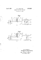
- Fig. 1 illustrates one embodiment of the junction transistor oscillator of this invention
- Fig. 2 illustrates an alternative embodiment of the invention.
- P-N junction type transistors comprise a body of solid semiconductive material, as for instance germanium or silicon, having therein a thin zone of one type conductivity material in contact with two zones of opposite type conductivity material forming therewith rectifying or P-N junctions.
- P-N-P or NP-N junction transistors are denominated as P-N-P or NP-N junction transistors, depending upon the conductivity type of the various zones.
- Such devices have broad area contact between opposite type conductivity regions as compared to the point contact type transistor, in which a region of one conductivity type is contacted by two points or line contact electrodes which form small area rectifying contacts with the semiconductor body.
- a P-N junction transistor such as may be used in this invention is described in vol. 40, Proceedings of the I. R. E., p. 1355 (Nov., 1952), Fused Impurity P-N-P Junction Transistor, by John S. Saby.
- an oscillator circuit must include a signal translating device having a negative resistance characteristic, or alternatively a regenerative feedback path must be provided between the output and input of the signal translating device used.
- Point contact semiconductor transistor may-be readily.
- the input resistance of a point contact transistor is composed of two components, the first of which is an. inherently negative resistancedue to the current multiplication (amplification) characteristic of the point contact transistor.
- the second component comprises an inherently positive resistance due to the resistance of the point contact and the resistance of the bulk semiconductor material of which the device is constructed.
- Both of the above components of the input resistance of a point contact transistor may be varied by varying the collector and emitter voltages respectively. By so doing, a negative resistance characteristic may easily be obtained and thus the point contact type transistor may readily serve as a component of a transistor oscillator circuit.
- P-N junction transistors have been proven to be quite superior to point contact transistors for a number of reasons, among which are their relatively low noise figure, their freedom from short-circuit instability, their higher power handling capacity, and ease of operation with.- small power consumption.
- transistor circuit components be junction type rather than point contact type.
- point contact transistors having an inherent negative resistance characteristic due to their amplification char acteristics, readily serve as components for transistor oscil' lator circuits
- the P-N junction type transistor has a current amplification which is always less than unity. Because of this lack of current amplification, junction transistors are unconditionally stable at low frequencies, and do not present negative resistance characteristics.
- junction transistor oscillator circuits may be provided by employing external circuit components which supply regenerative feedback between the output and the input of the junction transistor. This expedient, however, adds complexity to the circuit.
- I provide a junction transistor oscillator circuit having a minimum number of circuit elements and less complexity than transistor oscillator circuits which employ regenerative feedback elements. This is accomplished by adjusting the external emitter to base impedance thus causing the transistor to exhibit an effective negative resistance characteristic at high frequencies.
- the three terminal junction transistors utilized in the present invention are not to be confused with certain two terminal junction semiconductor devices which may show negative resistance due to transit time effects.
- the latter devices develop a negative resistance by having an extremely long transit time corresponding to a transit angle of greater than 180.
- Such large transit angles are not consistent with transistor action, which requires, for satisfactory operation, a transit time corresponding to a transit angle of less than Thus, it. would not be possible to utilize the transit time effect to cause a three terminal junction transistor to exhibit a negative resistance.
- the impedances of a junction transistor may be considered to be purely resistive. However, .at higher frequencies, theimpedances become complex in nature. 11 have found that when the transistor circuit parameters are chosen so that the external emitter to base impedance is capacitive reactance, the tnansistor may be made to exhibit a negative resistance between collector and base. The transistor may then serve as an oscillator component without an external regenenat'ivefeedback circuit.
- i1 is the current flowing in the emitter-base circuit
- 22 is the collector-base volt age
- i2. is the current flowing in the collector-base circuit.
- each. of the h parameters may be determined experimentally for any given junction transistor by appropriate measurements by determining the desired values of current and voltage as indicated by the above relationships defining the panameters (Equations 3 to 6). -It is to be understood that these parameters will vary for each transistor and are dependent upon the size, eonfiguration, and other physical constants of the transistor itself.
- the measured voltages and currents also have reactive components and the corresponding h parameters become reactive with increasing frequency.
- the frequency at which a particular transistor impedance shows reactive components also depends upon the configuration, size, and other physical constants of the transistor.
- Z1 the external impedance connected between emitter and base
- Z1 may be a capacitor having a capacitive C1 and may be selected so that the reactance thereof is greater than ]h11
- a negative resistance oscillator may be made by connecting between collector and base terminals an impedance having an efiiective positive shunt conductance with an absolute magnitude less than that of the effective negative shunt conductance Gout.
- the impedance which is connected between collector and base may conveniently be a parallel resonant LC circuit in which the capacitive element C2 may be used to adjust the frequency of oscillation.
- an inductance may be used, in which case the resonant circuit for the transistor oscillator comprises the inductance and the natural capacitance of the transistor.
- the frequency of oscillation may be regulated by adjusting the value of L the inductance.
- P-type zone 2 is extremely thin, of the order of 0.001 inch or less, and forms rectifyingP-N junctions 5 and 6 with N-type zones 3 and 4 respectively.
- Transistor 1 may conveniently be cut from a single crystal of a semiconductor material, as for instance germanium or silicon, grown by seed crystal withdrawal during which the rate of growth is varied in order to produce PN junctions 5 and 6. The method of growing such crystals is disclosed and claimed in the copending application of Robert N. Hall, Serial No. 304,203, filed August 13, 1952, and assigned to the same assignee as the present invention.
- a low resistance contact to N-type zone 3 is made by fusion or soldering of a donor material which may conveniently be an alloy of indium and 1% to 10% by weightof arsenic or antimony, to form an emitter contact 7.
- a low resistance contact of the same composition may be fused to N-type zone 4 to form a collector contact 8.
- a low resistance contact to P-type zone 2 may conveniently be made by fusing, at high temperature, an indium dot to P-type region 2 to form a base contact 9.
- Base contact 9 is grounded to form a grounded base circuit, and the emitter bias voltage is applied, in the forward direction, through high impedance coil 10, between emitter (7) and base (9) by battery 11.
- the collector bias voltage is applied, in the reverse direction, between the collector 8 and base 9 by battery 12
- the output of the transistor appears between terminals 13.
- a transistor emitter or collector region may be said to be biased in the forward direction when the polarity of the biasing voltage applied to that region bears the same sign as the sign of the majority conduction carriers contained therein and conventional current flows into the region.
- an emitter or collector may be said to be biased in the reverse direction when the polarity of the biasing voltage bears the opposite sign of the majority conduction carriers contained therein, and conventional current flows out from the region.
- Capacitor 14 is connected across the input between emitter and base, and hasa value so that the impedance [Z1], which is equal to is greater than in; and is sufiiciently large as to cause the output conductance Gout. to the negative according to the aforementioned relationship, Equation 7.
- a parallel resonant circuit 15 comprising'capacitor (C2), .16, and inductance (L), 17, chosen so that the admittance of the resonant circuit has a negative (inductive) phase angle and a conductance less than the value of Gout in Equation 7, is connected between base 9 and collector 8.
- the frequency of oscillation of the circuit is dependent upon the value of L and the combined values of C2 and the inherent capacitance of the transistor, and may be controlled by varying the value of capacitor 16.
- Fig. 2 of the diagram there is shown an alternative embodiment of the invention, in which the resonant circuit of the previous embodiment has been replaced by a simple inductive element 17.
- This embodiment relies upon the inherent capacitance of transistor 1 in order to form a resonant circuit in the output circuit.
- the frequency. of this embodiment will assume a natural frequency dependent upon the value of the inductance 17 and the natural capacitance of transistor 1.
- the frequency of oscillation may be varied by varying the inductance of inductor L.
- a negative resistance oscillator comprising a semiconductor signal translating device including a region of one conductivity type adjoining two regions of opposite conductivity type and forming broad area P-N junctions therewith, a base contact to said one conductivity type region, an emitter contact to one of said opposite conductivity type regions, and a collector contact to the remaining opposite conductivity .type region, a capacitive circuit connected between emitter and base contacts, an inductive network connected between collector and base contacts, means for biasing the emitter in the forward direction and means for biasing the collector in the reverse direction.
- a negative resistance oscillator comprising a three terminal semiconductor signal translating device having emitter, collector and base regions, a capacitive circuit connected between emitter and base, an inductive network connected between collector and base, means for biasing the emitter in the forward direction, and means for biasing the collector in the reverse direction.
- a negative resistance oscillator comprising a three terminal semiconductor signal translating device having emitter, collector and base regions, a capacitive circuit connected between emitter and base, said signal translating device and said capacitive circuit element exhibiting jointly a negative output conductance, an inductive network connected between collector and base, means for biasing the emitter in the forward direction, and means for biasing the collector in the reverse direction.
- a negative resistance oscillator comprising a three terminal semiconductor signal translating device having emitter, collector and base regions, a capacitive circuit between emitter and base, said signal translating device and said capacitive circuit element possessing jointly a negative output conductance, an inductive network connected between collector and base, said network possessing a positive conductance less than the absolute value of the output conductance of said signal translating device and said capacitive circuit element, means for biasing the emitter in the forward direction, and means for biasing the collector in the reverse direction.
- a negative resistance junction transistor oscillator comprising a three terminal junction transistor having emitter, collector and base regions, a capacitive circuit connected between said emitter and base, said transistor and said capacitive circuit element possessing a joint negative output conductance, an inductive network connected between said collector and base, means for biasing the emitterin the forward direction, and means for biasing the collector in the reverse direction.
- a negative resistance junction transistor oscillator comprising a three terminal junction transistor having emitter, collector and base regions, a capacitive circuit connected between said emitter and base, said capacitive circuit element and said transistor possessing a joint negative output conductance, an inductive network connected between said collector and base, said network possessing a positive conductance less than the absolute value of the output conductance of said transistor and capacitance circuit element, means for biasing the emitter in the forward direction and means for biasing the collector in the reverse direction.
- an inductive network connected between said collector and base, means for biasing the transistor emitter in the for- Ward direction, and means for biasing the transistor collector in the reverse direction.
Landscapes
- Inductance-Capacitance Distribution Constants And Capacitance-Resistance Oscillators (AREA)
Description
United States Patent '0 NEGATIVE RESISTANCE OSCILLATOR Robert L. Pritchard, Schenectady, N. Y., assignor to General Electric Company, a corporation of New York Application September 30, 1954, Serial No. 459,360
8 Claims. 01. 250-36 This invention relates to transistor oscillator circuits, and more particularly to junction transistor oscillator circuits.
An object of this invention is to provide a junction transistor oscillator circuit for high frequency operation.
A further object of the invention is to provide a junction transistor oscillator circuit which does not require an external feedback circuit element.
Another object of the invention is to provide a junction transistor oscillator circuit of less complexity than junction transistor oscillator circuits obtainable heretofore.
A still further object of the invention is to provide a junction transistor oscillator circuit utilizing a junction transistor having a negative resistance at high frequencies.
Briefly stated, in accordance with a broad aspect of this invention, a junction transistor oscillator circuit is provided for high frequency operation by adjusting the circuit parameters so that the junction transistor exhibits a negative conductance, and connecting a circuit component which exhibits an effective positive shunt conductance between the collector the base terminals.
The novel features believed characteristic of the invention are set forth in the appended claims. The invention itself, however, together with further objects and advantages thereof, may best be understood by reference to following description taken in connection with the drawing, in which:
Fig. 1 illustrates one embodiment of the junction transistor oscillator of this invention, and
Fig. 2 illustrates an alternative embodiment of the invention.
This invention utilizes, as its central component, a three terminal semiconductor signal translating device which has come to be known in the art as a P-N junction type transistor. P-N junction type transistors comprise a body of solid semiconductive material, as for instance germanium or silicon, having therein a thin zone of one type conductivity material in contact with two zones of opposite type conductivity material forming therewith rectifying or P-N junctions. These devices are denominated as P-N-P or NP-N junction transistors, depending upon the conductivity type of the various zones. Such devices have broad area contact between opposite type conductivity regions as compared to the point contact type transistor, in which a region of one conductivity type is contacted by two points or line contact electrodes which form small area rectifying contacts with the semiconductor body. A P-N junction transistor such as may be used in this invention is described in vol. 40, Proceedings of the I. R. E., p. 1355 (Nov., 1952), Fused Impurity P-N-P Junction Transistor, by John S. Saby.
According to well accepted oscillator theory, an oscillator circuit must include a signal translating device having a negative resistance characteristic, or alternatively a regenerative feedback path must be provided between the output and input of the signal translating device used. Point contact semiconductor transistormay-be readily.
made to supply a negative resistance characteristic. This is so because the input resistance of a point contact transistor is composed of two components, the first of which is an. inherently negative resistancedue to the current multiplication (amplification) characteristic of the point contact transistor. The second component comprises an inherently positive resistance due to the resistance of the point contact and the resistance of the bulk semiconductor material of which the device is constructed. Both of the above components of the input resistance of a point contact transistor may be varied by varying the collector and emitter voltages respectively. By so doing, a negative resistance characteristic may easily be obtained and thus the point contact type transistor may readily serve as a component of a transistor oscillator circuit.
P-N junction transistors have been proven to be quite superior to point contact transistors for a number of reasons, among which are their relatively low noise figure, their freedom from short-circuit instability, their higher power handling capacity, and ease of operation with.- small power consumption. For these, and other rea-- sons, it is desirable that transistor circuit components be junction type rather than point contact type. Whereas point contact transistors having an inherent negative resistance characteristic, due to their amplification char acteristics, readily serve as components for transistor oscil' lator circuits, the P-N junction type transistor has a current amplification which is always less than unity. Because of this lack of current amplification, junction transistors are unconditionally stable at low frequencies, and do not present negative resistance characteristics. However, junction transistor oscillator circuits may be provided by employing external circuit components which supply regenerative feedback between the output and the input of the junction transistor. This expedient, however, adds complexity to the circuit. According to this invention, I provide a junction transistor oscillator circuit having a minimum number of circuit elements and less complexity than transistor oscillator circuits which employ regenerative feedback elements. This is accomplished by adjusting the external emitter to base impedance thus causing the transistor to exhibit an effective negative resistance characteristic at high frequencies.
The three terminal junction transistors utilized in the present invention, and caused to exhibit negative resistances to permit negative resistance oscillator operation, are not to be confused with certain two terminal junction semiconductor devices which may show negative resistance due to transit time effects. The latter devices develop a negative resistance by having an extremely long transit time corresponding to a transit angle of greater than 180. Such large transit angles are not consistent with transistor action, which requires, for satisfactory operation, a transit time corresponding to a transit angle of less than Thus, it. would not be possible to utilize the transit time effect to cause a three terminal junction transistor to exhibit a negative resistance.
At low frequencies, the impedances of a junction transistor may be considered to be purely resistive. However, .at higher frequencies, theimpedances become complex in nature. 11 have found that when the transistor circuit parameters are chosen so that the external emitter to base impedance is capacitive reactance, the tnansistor may be made to exhibit a negative resistance between collector and base. The transistor may then serve as an oscillator component without an external regenenat'ivefeedback circuit.
For a more complete description of the teaching of i this invention, by which a negative resistance may the obta-inedbetween collector and base terminalsof ajunc tion transistor, use will be made of the grounded base, series parallel, small signal, 11 parameters. The small signal series parallel 11 parameters are well known to the art and a thorough description thereof may be found in Small Signal Parameters for Transistors by R. L. P-ritchard, to be published in the October 1954 issue of Electr-ical Engineering.
The series parallel or 11 parameters are defined by the equations:
where 01 is the emitter-base voltage, i1 is the current flowing in the emitter-base circuit, 22 is the collector-base volt age, and i2. is the current flowing in the collector-base circuit. The 12 parameters are further defined as the following:
(3) It (short circuit input impedance) =E-whon :0
(1) In: (the open circuit voltage feedback ratio)=? 2 when t (5) In, (the short circuit current transfer ratio)=%- I when 0 O and (G) 71 (the open circuit output admittunce)=% when 1 0 (7) n-lr) In Equation 7, each. of the h parameters may be determined experimentally for any given junction transistor by appropriate measurements by determining the desired values of current and voltage as indicated by the above relationships defining the panameters (Equations 3 to 6). -It is to be understood that these parameters will vary for each transistor and are dependent upon the size, eonfiguration, and other physical constants of the transistor itself. For a detailed discussion of the Mariation of small signal 11 parameters of junction transistors as a function of such physical transistor variable as dilfusion length, difiusion constant, base width, barrier capacitance, bias, concentration of minority carriers in the base region, and others, reference is herein made to the article, Frequency Variation of Junction Transistor Parameters, by Richard L. Pritchard, in vol. 42, No. 5, page .786, Proceedings of the I. R. B, May 1954. Since each h parameter is representative of :a relationship between voltage and/or current, these parameters may, at low frequencies, at which the transistor impedances are essentially resistive, represent only real components. How ever, at higher frequencies, at which the tnansistor impedances cease to be real only, and possessreactive components, the measured voltages and currents also have reactive components and the corresponding h parameters become reactive with increasing frequency. The frequency at which a particular transistor impedance shows reactive components also depends upon the configuration, size, and other physical constants of the transistor.
For a detailed discussion of the variation of It parameters with frequency, reference is herein made to the article Small Signal Parameters of Grown Junction Transistors at High Frequency, by Robert L. Pritchard and W. N. Coffey, Convention Record of the I. R. E., vol. 2, Part 3 (1954), p. 89. At low frequencies, therefore, all of the 11 parameters of Equation 7 are real and the resultant admittance Yout is real. Because the quantity is always greater than 0, in the purely resistive case at low frequency, the output admittance is always real and greater than hzz. With increasing frequency both I122 and 1112 become positive reactive, having phase angles of the order of to degrees. Additionally 1111 increases in magnitude and also becomes positive reactive having a positive phase angle, while hz1 becomes negative reactive and therefore has a negative phase angle. For any given junction transistor, at :a given high frequency, at which the 11 parameters cease to be purely resistive and possess a reactive component, Z1 (the external impedance connected between emitter and base) may be a capacitor having a capacitive C1 and may be selected so that the reactance thereof is greater than ]h11|. When this condition is satisfied, the quantity Z1+h11 will have a negative reactive component. If the valueof IZiI chosen (which will equal since the impedance Z1 chosen is capacitive is large enough, the term l1'i' l will have a phase angle in excess of 90 degrees and therefore a negative conductance. When this negative real component exceeds the positive real component of 1122, the real component Gout, of Yout is negative.
As an example of the above relationship, the following values for h parameters taken firom a typical transistor having a base spreading resistance of 300 ohms, an a cut olf frequency of 5 megacycles, a collector capacitance of 10 an id. operated at a frequency of 1 megacycle, areas follows:
These values inserted into the equation for output aclmittance, Equation 7, give the value of From this value it may be seen that the real component (conductance) is equal to Gout=-l56 (l0 mhos. Thus, the junction transistor and the associated capacitive shunt across the emitter to base terminal display a negative conductance. A negative resistance oscillator may be made by connecting between collector and base terminals an impedance having an efiiective positive shunt conductance with an absolute magnitude less than that of the effective negative shunt conductance Gout. The impedance which is connected between collector and base may conveniently be a parallel resonant LC circuit in which the capacitive element C2 may be used to adjust the frequency of oscillation. Alternatively, an inductance may be used, in which case the resonant circuit for the transistor oscillator comprises the inductance and the natural capacitance of the transistor. In this case the frequency of oscillation may be regulated by adjusting the value of L the inductance.
In Fig. 1 of the diagram there is shown one embodiment of the invention, including a P-N junction transistor 1 having a P-type zone 2 contiguous with two N- type zones 3 and 4 respectively. P-type zone 2 is extremely thin, of the order of 0.001 inch or less, and forms rectifyingP-N junctions 5 and 6 with N- type zones 3 and 4 respectively. Transistor 1 may conveniently be cut from a single crystal of a semiconductor material, as for instance germanium or silicon, grown by seed crystal withdrawal during which the rate of growth is varied in order to produce PN junctions 5 and 6. The method of growing such crystals is disclosed and claimed in the copending application of Robert N. Hall, Serial No. 304,203, filed August 13, 1952, and assigned to the same assignee as the present invention. A low resistance contact to N-type zone 3 is made by fusion or soldering of a donor material which may conveniently be an alloy of indium and 1% to 10% by weightof arsenic or antimony, to form an emitter contact 7. Likewise, a low resistance contact of the same composition may be fused to N-type zone 4 to form a collector contact 8. A low resistance contact to P-type zone 2 may conveniently be made by fusing, at high temperature, an indium dot to P-type region 2 to form a base contact 9. Base contact 9 is grounded to form a grounded base circuit, and the emitter bias voltage is applied, in the forward direction, through high impedance coil 10, between emitter (7) and base (9) by battery 11. The collector bias voltage is applied, in the reverse direction, between the collector 8 and base 9 by battery 12 The output of the transistor appears between terminals 13. A transistor emitter or collector region may be said to be biased in the forward direction when the polarity of the biasing voltage applied to that region bears the same sign as the sign of the majority conduction carriers contained therein and conventional current flows into the region. Conversely, an emitter or collector may be said to be biased in the reverse direction when the polarity of the biasing voltage bears the opposite sign of the majority conduction carriers contained therein, and conventional current flows out from the region.
As an example of same values of L and C2 which may be used in the circuit of Fig. 1 to construct a negative resistance junction transistor oscillator in accordance with the invention, the following illustration is given. Using a typical N-P-N junction transistor, an external emitterbase capacitance of 0.1 mid, and an inductance (L) of 25 millihenries, oscillation was obtained over a range of values of C2 (capacitor 16), varying from 80 to 200 micro-mid. This corresponds to a frequency range of from 100 to 500 kilocycles. Other circuit element values for which oscillations were obtained are listed in the following table in which C1 =external emitter-base capacitance, in microfarads L =external collector-base inductance, in Inillihenries O'z=external collector-base capacitance, inmicrofarads F= frequency of oscillations It is to beappreciated that the foregoing data are given as examples only and are not to be interpreted as limiting the invention to the particular values given.
In Fig. 2 of the diagram there is shown an alternative embodiment of the invention, in which the resonant circuit of the previous embodiment has been replaced by a simple inductive element 17. This embodiment relies upon the inherent capacitance of transistor 1 in order to form a resonant circuit in the output circuit. The frequency. of this embodiment will assume a natural frequency dependent upon the value of the inductance 17 and the natural capacitance of transistor 1. The frequency of oscillation, however, may be varied by varying the inductance of inductor L.
While the above circuit has been described with respect to an NP-N junction transistor, it is to be appreciated that a PNP transistor could be used as well, in which case the polarity of the applied bias voltage would be reversed. This minor change would in no way affect the operation of the device, and it would still function as a grounded base, negative resistance junction transistor oscillator.
While the invention has been described with respect to a particular embodiment, it will be understood that many changes and modifications may be made by those skilled in the art without departing from my invention. Therefore, by the appended claims, I intend to cover all such changes and modifications as fall within the true spirit and scope of the invention.
What I claim as new and desire to secure by Letters Patent of the United States is:
1. A negative resistance oscillator comprising a semiconductor signal translating device including a region of one conductivity type adjoining two regions of opposite conductivity type and forming broad area P-N junctions therewith, a base contact to said one conductivity type region, an emitter contact to one of said opposite conductivity type regions, and a collector contact to the remaining opposite conductivity .type region, a capacitive circuit connected between emitter and base contacts, an inductive network connected between collector and base contacts, means for biasing the emitter in the forward direction and means for biasing the collector in the reverse direction.
2. A negative resistance oscillator comprising a three terminal semiconductor signal translating device having emitter, collector and base regions, a capacitive circuit connected between emitter and base, an inductive network connected between collector and base, means for biasing the emitter in the forward direction, and means for biasing the collector in the reverse direction.
3. A negative resistance oscillator comprising a three terminal semiconductor signal translating device having emitter, collector and base regions, a capacitive circuit connected between emitter and base, said signal translating device and said capacitive circuit element exhibiting jointly a negative output conductance, an inductive network connected between collector and base, means for biasing the emitter in the forward direction, and means for biasing the collector in the reverse direction.
4. A negative resistance oscillator comprising a three terminal semiconductor signal translating device having emitter, collector and base regions, a capacitive circuit between emitter and base, said signal translating device and said capacitive circuit element possessing jointly a negative output conductance, an inductive network connected between collector and base, said network possessing a positive conductance less than the absolute value of the output conductance of said signal translating device and said capacitive circuit element, means for biasing the emitter in the forward direction, and means for biasing the collector in the reverse direction.
5. A negative resistance junction transistor oscillator comprising a three terminal junction transistor having emitter, collector and base regions, a capacitive circuit connected between said emitter and base, said transistor and said capacitive circuit element possessing a joint negative output conductance, an inductive network connected between said collector and base, means for biasing the emitterin the forward direction, and means for biasing the collector in the reverse direction.
6. A negative resistance junction transistor oscillator comprising a three terminal junction transistor having emitter, collector and base regions, a capacitive circuit connected between said emitter and base, said capacitive circuit element and said transistor possessing a joint negative output conductance, an inductive network connected between said collector and base, said network possessing a positive conductance less than the absolute value of the output conductance of said transistor and capacitance circuit element, means for biasing the emitter in the forward direction and means for biasing the collector in the reverse direction.
7. A negative resistance junction transistor oscillator comprising a three terminal junction transistor having emitter, collector, and base regions, a capacitive circuit connected between said emitter and base, the value of said element being such that the real component of the joint output admittance of said transistor and said circuit element as defined by the equation Yard/227m is negative at frequencies at which the impedances of said transistor possess reactive components, where e h when 0 when e =O 1'11 7 tit and
e1=Transistor emitter-base alternating current voltage ez=Transistor collector-base alternating current voltage i1=Transistor emitter current i2=Transistor collector current,
an inductive network connected between said collector and base, means for biasing the transistor emitter in the for- Ward direction, and means for biasing the transistor collector in the reverse direction.
8. A negative resistance junction transistor oscillator comprising a three terminal junction transistor having emitter, collector, and base regions, a capacitive circuit connected between said emitter and base, the value of said element being such that the real component of the joint output admittance of saidtransistor and said circuit element as defined by the equation h 2.h n-i-ZI) is negative at frequencies at which the impedance of said transistor possess reactive components, where and e1=Transistor emitter base alternating current voltage ez=Transistor collector base alternating current voltage i1=Transistor emitter current iz Transistor collector current,
References Cited in the file of this patent UNITED STATES PATENTS Kuhn Feb. 2, 1926 Shockley Sept. 25, 1951 OTHER REFERENCES Article: Junction Transistor Equivalent Circuits and Vacuum Tube Analogy, by Giacoletto, pages 1490- 1493 of Proc. 1. R. B, vol. 40, No. 11 of November 1952.
Priority Applications (3)
| Application Number | Priority Date | Filing Date | Title |
|---|---|---|---|
| US459360A US2777065A (en) | 1954-09-30 | 1954-09-30 | Negative resistance oscillator |
| GB27000/55A GB802104A (en) | 1954-09-30 | 1955-09-21 | Improvements relating to transistor oscillator circuits |
| FR1131775D FR1131775A (en) | 1954-09-30 | 1955-09-30 | Transistron oscillator |
Applications Claiming Priority (1)
| Application Number | Priority Date | Filing Date | Title |
|---|---|---|---|
| US459360A US2777065A (en) | 1954-09-30 | 1954-09-30 | Negative resistance oscillator |
Publications (1)
| Publication Number | Publication Date |
|---|---|
| US2777065A true US2777065A (en) | 1957-01-08 |
Family
ID=23824460
Family Applications (1)
| Application Number | Title | Priority Date | Filing Date |
|---|---|---|---|
| US459360A Expired - Lifetime US2777065A (en) | 1954-09-30 | 1954-09-30 | Negative resistance oscillator |
Country Status (3)
| Country | Link |
|---|---|
| US (1) | US2777065A (en) |
| FR (1) | FR1131775A (en) |
| GB (1) | GB802104A (en) |
Cited By (5)
| Publication number | Priority date | Publication date | Assignee | Title |
|---|---|---|---|---|
| US2869084A (en) * | 1956-07-20 | 1959-01-13 | Bell Telephone Labor Inc | Negative resistance semiconductive device |
| US2910653A (en) * | 1956-10-17 | 1959-10-27 | Gen Electric | Junction transistors and circuits therefor |
| US3029642A (en) * | 1954-12-22 | 1962-04-17 | Standard Oil Co | Transistor thermistor telemetering device |
| US3263085A (en) * | 1960-02-01 | 1966-07-26 | Rca Corp | Radiation powered semiconductor devices |
| US3290613A (en) * | 1963-02-25 | 1966-12-06 | Rca Corp | Semiconductor signal translating circuit |
Citations (2)
| Publication number | Priority date | Publication date | Assignee | Title |
|---|---|---|---|---|
| US1571278A (en) * | 1921-08-26 | 1926-02-02 | Westinghouse Electric & Mfg Co | Connection for producing oscillations with vacuum tubes |
| US2569347A (en) * | 1948-06-26 | 1951-09-25 | Bell Telephone Labor Inc | Circuit element utilizing semiconductive material |
-
1954
- 1954-09-30 US US459360A patent/US2777065A/en not_active Expired - Lifetime
-
1955
- 1955-09-21 GB GB27000/55A patent/GB802104A/en not_active Expired
- 1955-09-30 FR FR1131775D patent/FR1131775A/en not_active Expired
Patent Citations (2)
| Publication number | Priority date | Publication date | Assignee | Title |
|---|---|---|---|---|
| US1571278A (en) * | 1921-08-26 | 1926-02-02 | Westinghouse Electric & Mfg Co | Connection for producing oscillations with vacuum tubes |
| US2569347A (en) * | 1948-06-26 | 1951-09-25 | Bell Telephone Labor Inc | Circuit element utilizing semiconductive material |
Cited By (5)
| Publication number | Priority date | Publication date | Assignee | Title |
|---|---|---|---|---|
| US3029642A (en) * | 1954-12-22 | 1962-04-17 | Standard Oil Co | Transistor thermistor telemetering device |
| US2869084A (en) * | 1956-07-20 | 1959-01-13 | Bell Telephone Labor Inc | Negative resistance semiconductive device |
| US2910653A (en) * | 1956-10-17 | 1959-10-27 | Gen Electric | Junction transistors and circuits therefor |
| US3263085A (en) * | 1960-02-01 | 1966-07-26 | Rca Corp | Radiation powered semiconductor devices |
| US3290613A (en) * | 1963-02-25 | 1966-12-06 | Rca Corp | Semiconductor signal translating circuit |
Also Published As
| Publication number | Publication date |
|---|---|
| GB802104A (en) | 1958-10-01 |
| FR1131775A (en) | 1957-02-27 |
Similar Documents
| Publication | Publication Date | Title |
|---|---|---|
| US2852677A (en) | High frequency negative resistance device | |
| US2816228A (en) | Semiconductor phase shift oscillator and device | |
| US2681996A (en) | Transistor oscillator | |
| US2840727A (en) | Self-locking transistor switching circuit | |
| US2791693A (en) | Stabilized semi-conductor oscillator circuits | |
| US2675474A (en) | Two-terminal sine wave oscillator | |
| US2757287A (en) | Stabilized semi-conductor oscillator circuit | |
| US2864062A (en) | Negative resistance using transistors | |
| US2570436A (en) | Crystal controlled oscillator | |
| US2895058A (en) | Semiconductor devices and systems | |
| US2777065A (en) | Negative resistance oscillator | |
| US3134949A (en) | Negative resistance frequency modulated oscillator | |
| US2559023A (en) | Phase modulation | |
| US2869084A (en) | Negative resistance semiconductive device | |
| US2930996A (en) | Active element impedance network | |
| US3416100A (en) | Voltage tuned oscillator with resistive and capacitive tuning diodes | |
| GB817268A (en) | Improvements in semiconductor networks | |
| US2750508A (en) | Transistor oscillator circuit | |
| US3054071A (en) | Polarity-sensitive negative resistance oscillator with frequency shift | |
| US3670183A (en) | Two-terminal negative resistance device employing bipolar-unipolar transistor combination | |
| US2910653A (en) | Junction transistors and circuits therefor | |
| US2769908A (en) | Negative impedance transistor circuits | |
| US2992399A (en) | Oscillator amplitude control | |
| US3157842A (en) | Multivibrator circuits using step recovery diodes as timing elements | |
| US3855552A (en) | Oscillator utilizing complementary transistors in a push-pull circuit |