US2777059A - Echo suppression beacons - Google Patents
Echo suppression beacons Download PDFInfo
- Publication number
- US2777059A US2777059A US220916A US22091651A US2777059A US 2777059 A US2777059 A US 2777059A US 220916 A US220916 A US 220916A US 22091651 A US22091651 A US 22091651A US 2777059 A US2777059 A US 2777059A
- Authority
- US
- United States
- Prior art keywords
- pulse
- beacon
- signal
- discriminator
- wave
- Prior art date
- Legal status (The legal status is an assumption and is not a legal conclusion. Google has not performed a legal analysis and makes no representation as to the accuracy of the status listed.)
- Expired - Lifetime
Links
- 230000001629 suppression Effects 0.000 title description 6
- 230000000903 blocking effect Effects 0.000 description 17
- 239000003990 capacitor Substances 0.000 description 13
- 238000010586 diagram Methods 0.000 description 11
- 230000005540 biological transmission Effects 0.000 description 7
- 230000000694 effects Effects 0.000 description 6
- 230000001960 triggered effect Effects 0.000 description 5
- 230000008878 coupling Effects 0.000 description 4
- 238000010168 coupling process Methods 0.000 description 4
- 238000005859 coupling reaction Methods 0.000 description 4
- 230000009429 distress Effects 0.000 description 4
- 238000005070 sampling Methods 0.000 description 3
- 241001270131 Agaricus moelleri Species 0.000 description 2
- 230000003111 delayed effect Effects 0.000 description 2
- 230000002349 favourable effect Effects 0.000 description 2
- 230000003213 activating effect Effects 0.000 description 1
- 230000003321 amplification Effects 0.000 description 1
- 239000013078 crystal Substances 0.000 description 1
- 238000001514 detection method Methods 0.000 description 1
- 238000011156 evaluation Methods 0.000 description 1
- 230000010354 integration Effects 0.000 description 1
- 230000002452 interceptive effect Effects 0.000 description 1
- 238000002955 isolation Methods 0.000 description 1
- 238000004519 manufacturing process Methods 0.000 description 1
- 238000003199 nucleic acid amplification method Methods 0.000 description 1
- 238000010587 phase diagram Methods 0.000 description 1
- 230000010287 polarization Effects 0.000 description 1
- 230000005855 radiation Effects 0.000 description 1
- 230000000630 rising effect Effects 0.000 description 1
- 230000035945 sensitivity Effects 0.000 description 1
- 230000008054 signal transmission Effects 0.000 description 1
- 239000002699 waste material Substances 0.000 description 1
Images


Classifications
-
- G—PHYSICS
- G01—MEASURING; TESTING
- G01S—RADIO DIRECTION-FINDING; RADIO NAVIGATION; DETERMINING DISTANCE OR VELOCITY BY USE OF RADIO WAVES; LOCATING OR PRESENCE-DETECTING BY USE OF THE REFLECTION OR RERADIATION OF RADIO WAVES; ANALOGOUS ARRANGEMENTS USING OTHER WAVES
- G01S13/00—Systems using the reflection or reradiation of radio waves, e.g. radar systems; Analogous systems using reflection or reradiation of waves whose nature or wavelength is irrelevant or unspecified
- G01S13/74—Systems using reradiation of radio waves, e.g. secondary radar systems; Analogous systems
- G01S13/76—Systems using reradiation of radio waves, e.g. secondary radar systems; Analogous systems wherein pulse-type signals are transmitted
- G01S13/767—Responders; Transponders
Definitions
- Beacons have been used at various geographical locations for transmitting coded pulsesjwhich identify the respective locations of thosebeacons. Itis considered undesirable that. the beacon should operate continuously, not only because of the waste entailed, but also because of the disturbing. effect ofthe beacon signals onradar screens in the area. This will be understoodfroni the manner of operation of radar beacons.
- the radar beacon is used to send a coded signal at a frequency corresponding to that of a mobile radar set so that the signal of. the beacon will visually appear on the cathode-ray screen of the mobile radar.
- the direction and range of the beacon are represented on the radar screen in a manner, very similar to the. representation of an object-reflection signal on, the radar screen,,that is to say, on the so-called' PPL screenv for example there willappear a code signal at an angular position representing the direction of the beacon; from the mobile radar unit and the radial position of the beacon code: signal will indicate approximatedistance between thebeacon and the radar unit. If the beacon were operating continuously and all other beacons similarly transmitted signals to all radar units within.
- beacons have been designed to respond only to a pulse of a length. different from that normally employed by radar units. In normal operation, the radar unit would transmit pulses of one micro-second duration, for; exampleg but. such radar units could be switched to 2 micro-second pulse operation for triggering beacons in the area. Should a lost aircraft switch to 2 micro-second radar pulses, there would appear on its radar screen a series of differently positioned beacon signals, coded to identify their respective locations.
- the aircraft is enabled to ascertain its position,.
- Beacons as a practical matter, are designed to operate over a very broad latitude of received signal strengths.
- a distant lost aircraft should be able to trigger the beacon and a close lost aircraft should also be able to trigger the beacon.
- the highgain beacon receiver tends to become over-loaded for strong signals and the pulses received tend to be selflimiting.
- One of" the purposes ofthe present invention accordingly, is to adaptbeacon receivers to. distinguish between triggering signals of a particular duration and combined signals of shorterduration which in combination simu? late triggering signals.
- the spurious signal which usually consists of a radar pulse and ⁇ its echo typically includes a strong first halfand a substantiall'yweaker. second half. Because this spurious signal is in most instances due to echo signals, the present invention has been entitled; Echo Suppression Beacons but, because of more general effectiveness, this title is not used. in any limiting sense.
- the beacon receiver conventionall'yincludes apulse length discriminator which causestriggering of the beacon transmitter in response to received signals of a. particular. length or duration.
- Spurious? signals simulate proper signals at the output of the pulse amplifier because of. the self-limiting characteristic of thatamplifier. 'LInIthe highgain amplifier, the distinctive wave-form of! spurious signals is obliterated;
- a further object of the invention. accordingly, is to enable beacon receivers'to. distinguish spurious signals from. true beacon. triggering signals. More specifically, an object. of the invention. is to. provide a beacon receiver with joint. control by a. pulse length discriminator andia system distinguishing. among difierent pulse wave-forms. In one aspect, therefore,
- the, invention provides. a. beacon. receiver for controlling;
- a beaconltransmittenlthe receiver containing a transmitter control circuit whose. operation. depends not only upon a pulse, length discriminator but also upon a wave for-m discriminator.
- this is achieved. by employing a plurality ofdetectors at. various points inv the. cascade. of amplifying. stages, so that at least one of these. detectors will receive asignal of adequate strength; and that signal will, nevertheless, retain its. original wave-form. before. limiting;
- signals are combined in such. a manner that any-departure from. theflan topped proper beacon-triggering signal is accentuated and this.'departureis utilized to suppress triggering of thebeacon transmitter by a spurious. pulseofthe same duration as a distress pulse, yet insure.bea-.
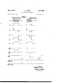
- Figure l is a diagram illustrating ordinary beacon operation and the production of spurious beacon-triggering' pulses,. and Figure. 1A illustrates an alternative form of spurious pulse; a
- FIG. 2 is the block diagram of a beacon receiver embodyingv features. of the presentinvention
- Figure 3 is a wiring diagram, partly a block diagram form, of a'portion of the receiver in Figure 2;
- Figure 4 is the wiring diagram of another portion of the receiver in Figure 2, includingthepulse length discriminator, and Figure 4A. is a. time diagram of pulses at various points in the pulse length discriminator of- Figure 4; I
- Figure 7 is a diagram of pulse wave-forms at difierent parts of the system of Figure 2.
- Figure 1 shows a beacon sending a code pulse after being triggered in response to distress signal (represented by the rectangular pulse form) from aircraft A.
- Aircraft B whose radar is operating normally, transmits a short pulse that combines with an echo signal from object C which pulse and echo combine typically to produce a complex wave-form such as that illustrated.
- the pulse and echo are presumed here to overlap and produce a wave-form that is, of necessity, not fiat-topped.
- Figure 1A Another wave-form is shown in Figure 1A which is produced when a short radar pulse and its echo are closely spaced 'but not in overlapping relation.
- Both of the wave-forms illustrated would appear substantially like that from aircraft A, after limiting in the beacon receiver; so that the beacon transmitter would be triggered.
- the beacon receiver is enabled to distinguish between pulses whose amplitudes vary, and fiat-topped pulses where both are of the same or nearly the same duration.
- Figure 2 there is shown a block diagram of the beacon from which the beacon transmitter has been omitted, that is to say, Figure 2 includes the beacon receiver and the control circuit for triggering the transmitter.
- the conventional beacon receiver includes mixer 10 for heterodyning signals from omni-directional antenna 12 with signals from local oscillator 14 to produce an intermediate frequency signal that is amplified in cascaded ampliers 161, 162 165. These amplifier stages in aggregate deliver signals to detector 18 to energize pulse length discriminator 19 for triggering the beacon transmitter in response to a received pulse of proper duration.
- the amplifier may, for example, be made up of a series of ten stages, each of which is a distributed amplifier and the cascade of stages is designed to produce a gain suflicient for operation in response to signals whose strength may vary at the beacon antenna from l 10- watts to X10 watts.
- the wave forms indicate a signal of intermediate strength that is properly amplified at the output of stage 162 so as to produce the true, unlimited wave form of useful amplitude at the output of detector 202.
- the output signals of detectors 20 are difierentiated in units 221, 222, 223, and 224 and the output signals of these diiferentiators are also illustrated in this block diagram by the coordinated wave-form representations.
- These differentiating signals are collected through diodes 241, 242, 243 and 244 which, in this instance, are polarized to pass the negative portions of the differentiatedoutput and to combine them for application (with suitable amplification) in the following control circuit.
- the control circuit includes a gate 26 whose output depends jointly on the combined input from collector diodes 24 and from the gating pulse generator 28 which, in turn, is energized by detector 18 through pulse delay device 30, advantageously an integrator that prevents operation of pulse generator 28 and of gate 26 in response to noise impulses of brief duration but insures slightly retarded operation of the gating pulse generator in re- 4 sponse to both spurious and proper radar pulses received by the beacon.
- Switch 26 is rendered efiective by pulse generator 28 to trigger a blocking signal generator 32 in the event that during the time interval of a proper pulse, there should be an output from the collectors demonstrating improper wave-form of the pulse and, hence, showing the received pulse to be spurious.
- Generator 32 produces no signal except in response to collectors 24 and pulse generator 28.
- a gate or switch 34 is provided for triggering the transmitter control unit 36 in response to output from pulse length discriminator 19 indicating a pulse of proper duration; but transmission through switch 34 is suppressed by a signal from blocking signal generator 32 in response to a received pulse of proper length but of spurious wave form.
- Switch 34 can also be arranged to suppress transmission from the pulse length discriminator to avoid triggering the transmitter in response to a particularly powerful radar unit in the immediate vicinity.
- Pulse form discriminator The pulse sampling detectors represented in the block diagram in Figure 2 may advantageously take the form shown in Figure 3.
- the detectors are seen to include resistors 401, 402, 403, and 404 across which the signal, amplified to various levels by respective cascade amplifier stages, is impressed. Additionally, detector 18 is illustrated, having an input signal applied to resistor 405.
- Series diodes 421, 422, 422, 424 and 425 transmit the demodulated pulse to load resistors 441, 442, 443, 444, and 445 through filters 461, 462, 463, 464, and 46 whose efiect is to prevent transmission or feedback of the carrier frequency energy.
- the detected and filtered pulses as sampled from the various amplifier stages are difierentiated by capacitors 481, 482, 483, and 48 and resistors 501, 502, 503 and 504. These difierentiators produce positive-going surge for each pulse increment and a negative-going surge for each pulse decrement.
- a series of diodes 521, 522, 523, and 524, connected to the differentiators, are polarized to pass only the negative surges of the difierentiators. These diodes are connected in common to output line 54 and to gate 26 in Figure 2 (see also Figure 5) through a suitable broad-band (video) amplifier 55 and output coupling condenser 55a.
- the efiect of diodes 52 is to pass the proper pulses for gate 26 ( Figure 2) but to prevent reverse .signal transmission from each of the detector channels reversely into the others.
- the multiple detector channels willdeliver a negative pulse to switch or gate 26 at the end of each pulse, and a negative pulse for each drop in pulse amplitude; but only if a negative pulse occurs within 2 micro-seconds of the positive or starting portion of the received pulse will be detector channels have the control effect to be described.
- the detector channels, the dilferentiators in those detector channels, and the collector diodes or combining network may be identified as a wave form discriminator because this combination produces no output during a fiat-top long pulse of the character intended to trigger the beacon transmitter but, in the event of any interruption or other decrement of pulse strength during an equally long pulse,
- the waveform discriminator contains plural channels coupled respectively to different signallevels in the cascaded amplifier, it is herein designated a multi-channel multi-level wave form discriminator.
- This portion of the circuit is. shown in Figure 4, receiving square-Wave pulses together with noise from video amplifier 55b and detector 425 ( Figure 3).
- the input signal is derived from the fifth detector channel ( Figures 2 and 3') so as who coupled through capacitors 56. to the grid 58 of a cathode follower stage 60. Between grid 58 and ground, there is a series circuit through diode 62 and capacitor 64,. the junction of this diode and capacitor being connected at top 66 of biasingvolttage divider 68, 70, the purpose of which is to render diode 62 non-conducting except when the signal reaches a value at which clipping or signal limiting is to be effected.
- the signal transmitted to grid 58 never exceeds a voltage that is accurately fixed by voltage divider 68, 70.
- This limiting is important because of the voltage sensitivity of the particular form of pulse length discriminator (to be described) that is used here.
- Diode 71 suppresses trailing reverse pulses at the ends of input signal pulses. These negative transients are due to limiting.
- cathode follower 60 The output of cathode follower 60 is impressed across a cathode load resistor 72 in series with a so-called tolerance delay line 74 forming part of'the pulse length discriminator.
- the limited pulse is also transmitted to the gate 26' ( Figure 2) through coupling capacitor 76, via. pulse delay device or integrator 30 and gating pulse generator 28 ( Figure 2) to be further described in connection with Figure 5.
- the pulses appearing at the cathode follower stage 60 are square waves of short or long duration, as is indicated in Figure 4'. However, the voltage across delay line '74 is modified, the signal rising to the maximum after a brief delay, and, after a fixed time interval, drops to zero. A reversezpulse of the same. duration is produced, commencin'g at the-end of the input square wave as is indicated at '78 qii1 Figure 4A.
- Figure 4A shows the voltage wave forms developed in the pulse length discriminator in response to signals of 1 micro-second, 2 micro-seconds, and 5 micro-seconds duration as those signals appear at capacitor 76, 78, and 86.
- This moditied signal is transmitted through coupling capacitor 78' to the grid 80 of a biased amplifier 82.
- which amplifier has a further delay line 84 as its load, the function of effect. of the delay lines is such that the bias' on the blocking oscillator. is never exceeded except for pulses whose length is a minimum fixed by basic delay line 84,
- Echo suppression control circuit In Figure 5, there is shown a specific illustrative portion of-the systemrepresented in Figure 2 by units 26, 28, 30, and 32.
- the input to the circuit of Figure 5 is received from capacitor 76 ( Figure 4) and is normally a square wave when the pulse is received, but, in the alternative, the input. signal might be highly amplified noise.
- This signal is impressed upon an integrator including resistor 92 in series with capacitor 94, the arrangement being such as to prevent substantialbuildup of voltage at the junction d6 of this integrator in response to noise but to insure adequate voltage in this junction in response to signal pulses.
- This pulse signal voltage is amplified by stage 98 and is impressed upon a mono-stable multithis being to furnish a basic delay perhaps 1.2 micronormally inoperative blocking oscillator 90 which is more or less conventional, but notfree running by virtue of negative bias on its grid.
- This biasv is overcome in response to each triggering pulse ( Figure 4A) to generate a control signal for trigger circuit 36 ( Figure 2) (subject to control by the pulse form discriminator) in.
- the latter is normally conducting. its cathode circuit includes a self-bias resistor 1045 and capacitor 108 in series with the crystal diode 11d and voltage dividing resistors 112 and 114.
- diode 118 is alscconducting and impresses a positive potential on junction 116 of diode 11d and resistor 112.
- the mono-vibrator 166' is reversed so as to make triode 102 conducting for a fixed time interval of perhaps 1.5- microseconds and cut ofi'the current through the triode 1G4.
- the voltage at junction 116 is approximately at ground potential, as insured by resistor 117.
- Diode 118 isconnected to diode but is polarized oppositely. This opposite polarization renders diode 118 non-conducting except when the mono-stable multivibrator has been triggered by a pulse, and diode 118 then remains conducting for only the time fixed by the multi-vibrator, 1.5 microseconds in'this illustration.
- Negative signals in the form of pulses are delivered through a suitable amplifier 55 from the wave-form discriminator ( Figure 3) through capacitor 55a ( Figure 5) and resistor 112' to diode 118. Negative pulses resulting from noise are blocked by diode 118 because at this stage diode 110 is conducting and diode 11% is non-conducting; but negative pulses from the waveform discriminator are permitted to pass diode 118 while triode 104 is non-conducting as is the case when a pulse (as disting-uished from noise) has been received. incidentally, pulses received at diode 118 during the brief time of integration of integrator 92, 94,. are suppressed.
- the negative. pulse transmitted by diode 118 is amplified and inverted by stage 122 and impressed as a positive triggering voltage on the blocking oscillator 124 which is normally blocked by negative bias.
- blocking oscillator 124 In response to the negative pulse through diode 118, blocking oscillator 124 generates a control pulse of long duration that is transmitted to a control circuit ( Figure 6) to be described.
- This control is, by design, made longer than that of the pulse length discriminator so that the effect of the pulse form discriminator will, with assurance, suppress operation of the beacon transmitter despite any tendency of the pulse length discriminator to trigger the transmitter.
- FIG. 6 there is shown a circuit whose purpose is to suppress operation of the beacon transmitter despite favorable length of pulse as determined by the pulse length discriminator, in the event that a spurious form of pulse is received rather than a flat-topped beacon triggering pulse.
- the circuit of Figure 6 essentially is a gate for transmitting triggering pulses from the pulse length discriminator ( Figure 4) to the beacon transmitter control circuit, but for disabling such transmission when a pulse is also delivered under control of the wave-form discriminator ( Figures 3 and 5).
- a brief positive-pulse output from the pulse length discriminator as produced by a blocking oscillator ( Figure 4) is applied through isolating resistor 126 to junction 123 of the gating circuit.
- a negative output pulse is transmitted from the blocking oscillator 124, that is triggered under proper conditions by the wave-form discriminator, through diode 130 and this pulse is of sufiicient duration and voltage amplitude to outlast and over-ride any pulse from the pulse length discriminator.
- Diode 132 is interposed between junction 128 and grid 134 of an amplifier 136. Diode 132 passes positive pulses only, such pulses coming via isolation resistor 126. Diode 132 presents high impedance to the negative blocking pulses from diode 130 so that this negative voltage is effective at junction 128. The lower-voltage positive pulses from resistor 126 are consequently ineffective.
- Amplified output from the pulse length discriminator appears at terminal 138 by virtue of load resistor 140 except when suppressed by a blocking signal.
- a very powerful normal radar signal of brief duration is received, immediately followed by its echo, the aggregate of which pulses are sufficiently intense to produce severe overloading of the beacon receiver and disturbance in the beacon receiver power supply.
- Such pulse may be expected from a radar set at the same location as the beacon.
- a signal can be derived from such radar set with a suitable pulse generator and applied to junction 128 as indicated for suppressing operation of the beacon transmitter despite the fact that the wave-form discriminator is disabled by the severe overload.
- a signal as received appears in amplifier stage 161 as represented in Figure 7 and may be either a beacon triggering pulse or it may be a spurious signal such as might be caused by a normal (short) radar signal with a trailing echo.
- the output of detector 18 appears as a square wave, both when a good pulse and when a spurious pulse is received.
- one of the detectors 201, 202, 20s, or 204 produces a. flat-topped wave for a good pulse and a suitably strong stepped wave for a spurious pulse.
- the output of the particular detector 20 that may be effective produces one positive surge and one negative surge at the output of its diiferentiator 22 in response to a good pulse, but one positive pulsefollowed by plural negative pulses are-produced in response to spurious forms of pulses.
- the normal radar pulse and its echo follow in quick' succession was to leave a time interval between them while still simulating a good pulse after limiting, or whether these normal and echo pulses overlap, there will always appear a negative pulse in the output of a dilferentiator 22 before the end of a 2 microsecond interval.
- This negative pulse is one in addition to the usual negative pulse at the end of a true beacontriggering signal.
- the extra, early negative pulse is transmitted by a collector diode24.
- Delay device or integrator 30 modifies the square'waves provided by detector 18 in response to both good and spurious pulses into a delayed and modified square wave as indicated.
- integrator 39 controls the gating pulse generator 23 (multi-vibrator 100) that is of perhaps 1.5 micro-seconds duration because of the delay introduced byinte rator 30 and. the tolerance desired at the end of the square wave pulse to suppress the normal negative pulse. It is of course undesirable for the negative pulse produced by the end of a proper square Wave pulse and transmitted by the'wavc-form discriminator to be transmitted through gate 26 ( Figure 2) and diode 113 ( Figure 5) for triggering the blocking oscillator 124. Such action might suppress proper operation of the beacon transmitter.
- gating pulse generator 28 it is desirable for gating pulse generator 28 to condition gate 26 (diode 118) to transmit a negative pulse at a time earlier than the trailing end of a received 2 micro-second pulse.
- the transmission of a negative pulse by gate 26 triggers gating pulse generator 32 (blocking oscillator 124 in Figure 5) and While pulse length discriminator 19 controls blocking oscillator 90 to produce a beacon triggering pulse for both good and spurious pulses, the gate 34 (13%, 132, 136) transmits a beacon triggering signal only in response to a good pulse as received. Response to a spurious pulse of the same duration such as may be synthesized by a shorter signal and its echo is suppressed.
- a beacon responsive to a long pulse and having means for suppressing response to combinations of shorter pulses including a cascade of amplifier stages having ample gain for limiting signals over a wide range of input signal lengths, a pulse length discriminator energized by the cascade of stages, a multiple channel wave-form discriminator the channels of Which are respectively coupled to different stages of the cascade amplifier, said channels including means responsive to deviations from constantamplitude pulses, a combining network energized by said deviation responsive means, and means jointly energized by the combining network and the pulse length discriminator for enabling beacon response to pulses of proper length whose level is substantially constant.
- a beacon responsive to a long pulse and having means for suppressing response to combinations of shorter pulses including in combination a pulse length discriminator, a cascade of amplifier stages, a Wave-form discriminator including multiple wave-form sampling channels connected separately to said amplifier stages, a combining network connected to said channels, and a control circuit rendered effective by said pulse length discriminator only in response to pulses of proper waveform and under control of the output of said combining network.
- a beacon selectively responsive to a long pulse of predetermined duration and having means for suppressing response to combinations of shorter pulses, including in combination a pulse length discriminator, a Wave-form discriminator having means eifective to detect departures from a flat-top Wave, a cascade of amplifier stages for energising said wave-form discriminator, said Wave-form discriminator including multiple Wave-form sampling channels connected separately to said amplifier stages, and a combining network connected to said channels, an output control circuit rendered efiective by said pulse length discriminator only in response to pulses of proper Waveform and under control of said Wave-form discriminator, and a gating circuit having delayed input coupling to said cascade of amplifier stages so as to be insensitive to brief noise pulses, said gating circuit having control connection to said output control circuit for enabling the Wave form 10 discriminator to disable said control circuit in the of detection of departures from a flat-top wave.
Landscapes
- Engineering & Computer Science (AREA)
- Radar, Positioning & Navigation (AREA)
- Remote Sensing (AREA)
- Computer Networks & Wireless Communication (AREA)
- Physics & Mathematics (AREA)
- General Physics & Mathematics (AREA)
- Radar Systems Or Details Thereof (AREA)
Description
Jan. 8, 1957. F. H. STITES 2,777,059
ECHO SUPPRESSION BEACONS Filed April 13, 1951 4 Sheets-Sheet 1 AMI, H AMI. H AMI? H'AMR H AMIZj 5 Z h Y f f g /8 I \R-C \nc 22 2-6 22 n-c E 5 015mm; l
25* 5 mmva PULSE mv. 55%;
, swarm Pl/lSfLEf/(rl'l/ 5% BMW/141M170? Fig.2 I 1" F Bloc/i216 521x51 INV TOR 34 FRANCIS E'snrss 554w BY TRANSM/I'it'k kw 79/662? C/(Z ATTORNEY 4 Jan. 8, 1957. F. H. STITES 2,777,059
. ECHO SUPPRESSION BEACONS Filed April 13, 1951 4 Sheets-Sheet 4 .v lg. 7 0/57/2555 5/6/V4L F spun/005 5/0041 (If? l/ v INVENTOR FRA/Vf/S ll. 57' I 7' E5 flu/(5 ATTORNEY United tates 2,777,059 ECHO SUPPRESSION BEACONS' Francis H. Stiles, Waylaud,. Mass., assignor to Sylvania Electric Products Inc., a corporation of Massachusetts The present invention relates to radio navigation systemsand, in particular, to beacons used inradio navigation in conjunctiontwith radar'units, e
Beacons have been used at various geographical locations for transmitting coded pulsesjwhich identify the respective locations of thosebeacons. Itis considered undesirable that. the beacon should operate continuously, not only because of the waste entailed, but also because of the disturbing. effect ofthe beacon signals onradar screens in the area. This will be understoodfroni the manner of operation of radar beacons.
The radar beacon is used to send a coded signal at a frequency corresponding to that of a mobile radar set so that the signal of. the beacon will visually appear on the cathode-ray screen of the mobile radar. The direction and range of the beacon are represented on the radar screen in a manner, very similar to the. representation of an object-reflection signal on, the radar screen,,that is to say, on the so-called' PPL screenv for example there willappear a code signal at an angular position representing the direction of the beacon; from the mobile radar unit and the radial position of the beacon code: signal will indicate approximatedistance between thebeacon and the radar unit. If the beacon were operating continuously and all other beacons similarly transmitted signals to all radar units within. their range, there would appear on all radar screens a large amount of unwanted beacon signal representations interfering with the. normal geographic or other radar pattern. To avoid. continuous beacon operation, beacons have been designed to respond only to a pulse of a length. different from that normally employed by radar units. In normal operation, the radar unit would transmit pulses of one micro-second duration, for; exampleg but. such radar units could be switched to 2 micro-second pulse operation for triggering beacons in the area. Should a lost aircraft switch to 2 micro-second radar pulses, there would appear on its radar screen a series of differently positioned beacon signals, coded to identify their respective locations. By
means, the aircraft is enabled to ascertain its position,.
and then resume normal 1 micro-second radar pulse transmission.
Beacons, as a practical matter, are designed to operate over a very broad latitude of received signal strengths. A distant lost aircraft should be able to trigger the beacon and a close lost aircraft should also be able to trigger the beacon. Withthese requirements the highgain beacon receiver tends to become over-loaded for strong signals and the pulses received tend to be selflimiting.
It is possible for two signals of l micro-second each to be received in rapid sequence or in overlapping relation atent ice Patented Jan, 8, 19.5.7
21 craft radar" and the reflectingobject are neareach other, and when the reflecting object is close to the beacon: The combined 1' micro-second and its echo simulate a 2 micro second distress signal in thebeacon receiver.
One of" the purposes ofthe present invention accordingly, is to adaptbeacon receivers to. distinguish between triggering signals of a particular duration and combined signals of shorterduration which in combination simu? late triggering signals.
The spurious signal which usually consists of a radar pulse and} its echo typically includes a strong first halfand a substantiall'yweaker. second half. Because this spurious signal is in most instances due to echo signals, the present invention has been entitled; Echo Suppression Beacons but, because of more general effectiveness, this title is not used. in any limiting sense.
The beacon receiver conventionall'yincludes apulse length discriminator which causestriggering of the beacon transmitter in response to received signals of a. particular. length or duration. Spurious? signals simulate proper signals at the output of the pulse amplifier because of. the self-limiting characteristic of thatamplifier. 'LInIthe highgain amplifier, the distinctive wave-form of! spurious signals is obliterated; A further object of the invention. accordingly, is to enable beacon receivers'to. distinguish spurious signals from. true beacon. triggering signals. More specifically, an object. of the invention. is to. provide a beacon receiver with joint. control by a. pulse length discriminator andia system distinguishing. among difierent pulse wave-forms. In one aspect, therefore,
the, invention, provides. a. beacon. receiver for controlling;
a beaconltransmittenlthe receiver. containing a transmitter control circuit whose. operation. depends not only upon a pulse, length discriminator but also upon a wave for-m discriminator. In. the illustrative embodiment, this is achieved. by employing a plurality ofdetectors at. various points inv the. cascade. of amplifying. stages, so that at least one of these. detectors will receive asignal of adequate strength; and that signal will, nevertheless, retain its. original wave-form. before. limiting; These. detected: signals are combined in such. a manner that any-departure from. theflan topped proper beacon-triggering signal is accentuated and this.'departureis utilized to suppress triggering of thebeacon transmitter by a spurious. pulseofthe same duration as a distress pulse, yet insure.bea-.
con operation in response to a true distress signal. These detectorsall produce. flattopped output signals in. response to true beacontriggering signals-and do notv intterfere with response of thebeacon to such signals.
The nature of the. invention: in the foregoing; aspects willbe better understood from the followingdetailed. description of an illustrative embodiment, considered in connection. with; the. accompanying drawings; and from thisdescription, further aspects of the invention and features of novelty will become apparent; In the accompanying drawings:
Figure l is a diagram illustrating ordinary beacon operation and the production of spurious beacon-triggering' pulses,. and Figure. 1A illustrates an alternative form of spurious pulse; a
Figure. 2 is the block diagram of a beacon receiver embodyingv features. of the presentinvention;
Figure 3 is a wiring diagram, partly a block diagram form, of a'portion of the receiver in Figure 2;
Figure 4 is the wiring diagram of another portion of the receiver in Figure 2, includingthepulse length discriminator, and Figure 4A. is a. time diagram of pulses at various points in the pulse length discriminator of- Figure 4; I
FiguresS -and 6'-are wiringdiagrams of additional portions' of FigureZ; and
Figure 7 is a diagram of pulse wave-forms at difierent parts of the system of Figure 2.
Referring now to the drawings, Figure 1 shows a beacon sending a code pulse after being triggered in response to distress signal (represented by the rectangular pulse form) from aircraft A. Aircraft B, whose radar is operating normally, transmits a short pulse that combines with an echo signal from object C which pulse and echo combine typically to produce a complex wave-form such as that illustrated. The pulse and echo are presumed here to overlap and produce a wave-form that is, of necessity, not fiat-topped. Another wave-form is shown in Figure 1A which is produced when a short radar pulse and its echo are closely spaced 'but not in overlapping relation. Both of the wave-forms illustrated would appear substantially like that from aircraft A, after limiting in the beacon receiver; so that the beacon transmitter would be triggered. By addition of a waveform discriminator to the usual beacon receiver and by integrating it into this combination, the beacon receiver is enabled to distinguish between pulses whose amplitudes vary, and fiat-topped pulses where both are of the same or nearly the same duration.
In Figure 2 there is shown a block diagram of the beacon from which the beacon transmitter has been omitted, that is to say, Figure 2 includes the beacon receiver and the control circuit for triggering the transmitter.
The conventional beacon receiver includes mixer 10 for heterodyning signals from omni-directional antenna 12 with signals from local oscillator 14 to produce an intermediate frequency signal that is amplified in cascaded ampliers 161, 162 165. These amplifier stages in aggregate deliver signals to detector 18 to energize pulse length discriminator 19 for triggering the beacon transmitter in response to a received pulse of proper duration.
In addition to this, there has been provided a system for deriving an adequately amplified signal, but, nonetheless unlimited signal, for control of the transmitter triggering device conjointly with the pulse length discriminator. In Figure 2, a number of detectors 201, 202, 203, and 204 are shown connected to corresponding amplifier stages 161, 162, 163, and 164. These produce the wave forms illustrated in response to the spurious signal of Figure 1. It is assumed that the spurious signal is of inadequate strength at the output of amplifier stage 161 to have any effect and that the gain of the amplifier is such that this signal is limited so as to be fiat topped at the output sides of amplifier stages 163, 164 and 165. The amplifier may, for example, be made up of a series of ten stages, each of which is a distributed amplifier and the cascade of stages is designed to produce a gain suflicient for operation in response to signals whose strength may vary at the beacon antenna from l 10- watts to X10 watts. In the block diagram in Figure 2, the wave forms indicate a signal of intermediate strength that is properly amplified at the output of stage 162 so as to produce the true, unlimited wave form of useful amplitude at the output of detector 202.
The output signals of detectors 20 are difierentiated in units 221, 222, 223, and 224 and the output signals of these diiferentiators are also illustrated in this block diagram by the coordinated wave-form representations. These differentiating signals are collected through diodes 241, 242, 243 and 244 which, in this instance, are polarized to pass the negative portions of the differentiatedoutput and to combine them for application (with suitable amplification) in the following control circuit.
The control circuit includes a gate 26 whose output depends jointly on the combined input from collector diodes 24 and from the gating pulse generator 28 which, in turn, is energized by detector 18 through pulse delay device 30, advantageously an integrator that prevents operation of pulse generator 28 and of gate 26 in response to noise impulses of brief duration but insures slightly retarded operation of the gating pulse generator in re- 4 sponse to both spurious and proper radar pulses received by the beacon.
Pulse form discriminator The pulse sampling detectors represented in the block diagram in Figure 2 may advantageously take the form shown in Figure 3. In this figure, the detectors are seen to include resistors 401, 402, 403, and 404 across which the signal, amplified to various levels by respective cascade amplifier stages, is impressed. Additionally, detector 18 is illustrated, having an input signal applied to resistor 405. Series diodes 421, 422, 422, 424 and 425 transmit the demodulated pulse to load resistors 441, 442, 443, 444, and 445 through filters 461, 462, 463, 464, and 46 whose efiect is to prevent transmission or feedback of the carrier frequency energy.
The detected and filtered pulses as sampled from the various amplifier stages are difierentiated by capacitors 481, 482, 483, and 48 and resistors 501, 502, 503 and 504. These difierentiators produce positive-going surge for each pulse increment and a negative-going surge for each pulse decrement. A series of diodes 521, 522, 523, and 524, connected to the differentiators, are polarized to pass only the negative surges of the difierentiators. These diodes are connected in common to output line 54 and to gate 26 in Figure 2 (see also Figure 5) through a suitable broad-band (video) amplifier 55 and output coupling condenser 55a. The efiect of diodes 52 is to pass the proper pulses for gate 26 (Figure 2) but to prevent reverse .signal transmission from each of the detector channels reversely into the others.
In operation, the multiple detector channels willdeliver a negative pulse to switch or gate 26 at the end of each pulse, and a negative pulse for each drop in pulse amplitude; but only if a negative pulse occurs within 2 micro-seconds of the positive or starting portion of the received pulse will be detector channels have the control effect to be described. In aggregate, the detector channels, the dilferentiators in those detector channels, and the collector diodes or combining network, may be identified as a wave form discriminator because this combination produces no output during a fiat-top long pulse of the character intended to trigger the beacon transmitter but, in the event of any interruption or other decrement of pulse strength during an equally long pulse,
manner to be furtherdetailed. And because the waveform discriminator, contains plural channels coupled respectively to different signallevels in the cascaded amplifier, it is herein designated a multi-channel multi-level wave form discriminator.
'Pulse length discriminator At this point, it may be well to digress somewhat to describe the pulse length discriminator energized by the complete cascade of amplifiers. This portion of the beacon receiver circuit is largely of a known form, but here it is modified. ior suppressing response to. noise, both for the pulse length discriminator and the pulse form discriminator.
This portion of the circuit is. shown in Figure 4, receiving square-Wave pulses together with noise from video amplifier 55b and detector 425 (Figure 3). The input signal is derived from the fifth detector channel (Figures 2 and 3') so as who coupled through capacitors 56. to the grid 58 of a cathode follower stage 60. Between grid 58 and ground, there is a series circuit through diode 62 and capacitor 64,. the junction of this diode and capacitor being connected at top 66 of biasingvolttage divider 68, 70, the purpose of which is to render diode 62 non-conducting except when the signal reaches a value at which clipping or signal limiting is to be effected. As a result, the signal transmitted to grid 58 never exceeds a voltage that is accurately fixed by voltage divider 68, 70. This limiting is important because of the voltage sensitivity of the particular form of pulse length discriminator (to be described) that is used here. Diode 71 suppresses trailing reverse pulses at the ends of input signal pulses. These negative transients are due to limiting.
The output of cathode follower 60 is impressed across a cathode load resistor 72 in series with a so-called tolerance delay line 74 forming part of'the pulse length discriminator. The limited pulse is also transmitted to the gate 26' (Figure 2) through coupling capacitor 76, via. pulse delay device or integrator 30 and gating pulse generator 28 (Figure 2) to be further described in connection with Figure 5.
The pulses appearing at the cathode follower stage 60 are square waves of short or long duration, as is indicated in Figure 4'. However, the voltage across delay line '74 is modified, the signal rising to the maximum after a brief delay, and, after a fixed time interval, drops to zero. A reversezpulse of the same. duration is produced, commencin'g at the-end of the input square wave as is indicated at '78 qii1 Figure 4A. (Figure 4A shows the voltage wave forms developed in the pulse length discriminator in response to signals of 1 micro-second, 2 micro-seconds, and 5 micro-seconds duration as those signals appear at capacitor 76, 78, and 86.) This moditied signal is transmitted through coupling capacitor 78' to the grid 80 of a biased amplifier 82. which amplifier has a further delay line 84 as its load, the function of effect. of the delay lines is such that the bias' on the blocking oscillator. is never exceeded except for pulses whose length is a minimum fixed by basic delay line 84,
" subject to a tolerance increase set by delay device 74.
For pulses within this latitude, there is developed a brief sharp excess substantially above the bias level of the blocking oscillator, due to a combination of pulses developed in the delay lines, only in response to such excessis the blocking oscillator triggered to emit a single pulse.
Echo suppression control circuit In Figure 5, there is shown a specific illustrative portion of-the systemrepresented in Figure 2 by units 26, 28, 30, and 32. The input to the circuit of Figure 5 is received from capacitor 76 (Figure 4) and is normally a square wave when the pulse is received, but, in the alternative, the input. signal might be highly amplified noise. This signal is impressed upon an integrator including resistor 92 in series with capacitor 94, the arrangement being such as to prevent substantialbuildup of voltage at the junction d6 of this integrator in response to noise but to insure adequate voltage in this junction in response to signal pulses. This pulse signal voltage is amplified by stage 98 and is impressed upon a mono-stable multithis being to furnish a basic delay perhaps 1.2 micronormally inoperative blocking oscillator 90 which is more or less conventional, but notfree running by virtue of negative bias on its grid. This biasv is overcome in response to each triggering pulse (Figure 4A) to generate a control signal for trigger circuit 36 (Figure 2) (subject to control by the pulse form discriminator) in.
response to a. pulse of prcdeterminedlength. The. opera tion of this pulse length discriminator is, described in greater detail'in volume 3 of the Radiation Laboratory Series Radar Beacons, page 186 (McGraw-I-Iil1)'. The
' The latter is normally conducting. its cathode circuit includes a self-bias resistor 1045 and capacitor 108 in series with the crystal diode 11d and voltage dividing resistors 112 and 114. In the absence of a signal when triode 104 is conducting, diode 118 is alscconducting and impresses a positive potential on junction 116 of diode 11d and resistor 112. Upon reception of apulse (as distinguished from noise by integrator 92', 94) the mono-vibrator 166' is reversed so as to make triode 102 conducting for a fixed time interval of perhaps 1.5- microseconds and cut ofi'the current through the triode 1G4.
During this time, the voltage at junction 116 is approximately at ground potential, as insured by resistor 117.
Negative signals in the form of pulses are delivered through a suitable amplifier 55 from the wave-form discriminator (Figure 3) through capacitor 55a (Figure 5) and resistor 112' to diode 118. Negative pulses resulting from noise are blocked by diode 118 because at this stage diode 110 is conducting and diode 11% is non-conducting; but negative pulses from the waveform discriminator are permitted to pass diode 118 while triode 104 is non-conducting as is the case when a pulse (as disting-uished from noise) has been received. incidentally, pulses received at diode 118 during the brief time of integration of integrator 92, 94,. are suppressed.
Assuming that a pulse has been received which is of the type intended to trigger the beacon transmitter, no
signal is received via capacitor 55a and, hence, no signal passes through diode 118 even though this diode is conducting during the. received pulse. If a pulseof short duration is received, operation of the beacon transmitter will not. result because of the control efiect of the pulselength discriminator and, hence, even though a negative pulse may pass through capacitor 55a and diode 113, such action ofithe wave-form discriminator and its output control circuit is of little importance. However, in the event that a pulse of proper duration is received, but is of varying amplitude (such as that resultingfrom abrief radar pulse with a trailing echo of that pulse) the wave-form discriminator produces a negative pulse while diode 118 isconducting and the following control is effected.
The negative. pulse transmitted by diode 118is amplified and inverted by stage 122 and impressed as a positive triggering voltage on the blocking oscillator 124 which is normally blocked by negative bias. In response to the negative pulse through diode 118, blocking oscillator 124 generates a control pulse of long duration that is transmitted to a control circuit (Figure 6) to be described. This control is, by design, made longer than that of the pulse length discriminator so that the effect of the pulse form discriminator will, with assurance, suppress operation of the beacon transmitter despite any tendency of the pulse length discriminator to trigger the transmitter.
PLD and PFD gating circuit In Figure 6 there is shown a circuit whose purpose is to suppress operation of the beacon transmitter despite favorable length of pulse as determined by the pulse length discriminator, in the event that a spurious form of pulse is received rather than a flat-topped beacon triggering pulse. The circuit of Figure 6 essentially is a gate for transmitting triggering pulses from the pulse length discriminator (Figure 4) to the beacon transmitter control circuit, but for disabling such transmission when a pulse is also delivered under control of the wave-form discriminator (Figures 3 and 5). A brief positive-pulse output from the pulse length discriminator as produced by a blocking oscillator (Figure 4) is applied through isolating resistor 126 to junction 123 of the gating circuit. A negative output pulse is transmitted from the blocking oscillator 124, that is triggered under proper conditions by the wave-form discriminator, through diode 130 and this pulse is of sufiicient duration and voltage amplitude to outlast and over-ride any pulse from the pulse length discriminator. Diode 132 is interposed between junction 128 and grid 134 of an amplifier 136. Diode 132 passes positive pulses only, such pulses coming via isolation resistor 126. Diode 132 presents high impedance to the negative blocking pulses from diode 130 so that this negative voltage is effective at junction 128. The lower-voltage positive pulses from resistor 126 are consequently ineffective.
Amplified output from the pulse length discriminator appears at terminal 138 by virtue of load resistor 140 except when suppressed by a blocking signal.
It may happen that a very powerful normal radar signal of brief duration is received, immediately followed by its echo, the aggregate of which pulses are sufficiently intense to produce severe overloading of the beacon receiver and disturbance in the beacon receiver power supply. Such pulse may be expected from a radar set at the same location as the beacon. A signal can be derived from such radar set with a suitable pulse generator and applied to junction 128 as indicated for suppressing operation of the beacon transmitter despite the fact that the wave-form discriminator is disabled by the severe overload.
Operation A review of the entire operation of the system may be appropriate and will be understood from the foregoing description in connection with Figures 3 to 6 inclusive but with special attention to Figure 2. The phase diagram appears in Figure 7 which identifies two forms of signal at various output points in Figure 2.
A signal as received appears in amplifier stage 161 as represented in Figure 7 and may be either a beacon triggering pulse or it may be a spurious signal such as might be caused by a normal (short) radar signal with a trailing echo. When amplified and inherently limited, the output of detector 18 appears as a square wave, both when a good pulse and when a spurious pulse is received. However, one of the detectors 201, 202, 20s, or 204 produces a. flat-topped wave for a good pulse and a suitably strong stepped wave for a spurious pulse. The output of the particular detector 20 that may be effective produces one positive surge and one negative surge at the output of its diiferentiator 22 in response to a good pulse, but one positive pulsefollowed by plural negative pulses are-produced in response to spurious forms of pulses. Whether the normal radar pulse and its echo follow in quick' succession was to leave a time interval between them while still simulating a good pulse after limiting, or whether these normal and echo pulses overlap, there will always appear a negative pulse in the output of a dilferentiator 22 before the end of a 2 microsecond interval. This negative pulse is one in addition to the usual negative pulse at the end of a true beacontriggering signal. The extra, early negative pulse is transmitted by a collector diode24.
Delay device or integrator 30 modifies the square'waves provided by detector 18 in response to both good and spurious pulses into a delayed and modified square wave as indicated. integrator 39 controls the gating pulse generator 23 (multi-vibrator 100) that is of perhaps 1.5 micro-seconds duration because of the delay introduced byinte rator 30 and. the tolerance desired at the end of the square wave pulse to suppress the normal negative pulse. It is of course undesirable for the negative pulse produced by the end of a proper square Wave pulse and transmitted by the'wavc-form discriminator to be transmitted through gate 26 (Figure 2) and diode 113 (Figure 5) for triggering the blocking oscillator 124. Such action might suppress proper operation of the beacon transmitter. However, it is desirable for gating pulse generator 28 to condition gate 26 (diode 118) to transmit a negative pulse at a time earlier than the trailing end of a received 2 micro-second pulse. The transmission of a negative pulse by gate 26 triggers gating pulse generator 32 (blocking oscillator 124 in Figure 5) and While pulse length discriminator 19 controls blocking oscillator 90 to produce a beacon triggering pulse for both good and spurious pulses, the gate 34 (13%, 132, 136) transmits a beacon triggering signal only in response to a good pulse as received. Response to a spurious pulse of the same duration such as may be synthesized by a shorter signal and its echo is suppressed.
What is claimed is:
l. A beacon responsive to a long pulse and having means for suppressing response to combinations of shorter pulses, including a cascade of amplifier stages having ample gain for limiting signals over a wide range of input signal lengths, a pulse length discriminator energized by the cascade of stages, a multiple channel wave-form discriminator the channels of Which are respectively coupled to different stages of the cascade amplifier, said channels including means responsive to deviations from constantamplitude pulses, a combining network energized by said deviation responsive means, and means jointly energized by the combining network and the pulse length discriminator for enabling beacon response to pulses of proper length whose level is substantially constant.
2. The combination of an input circuit, a pulse length discriminator and a wave-form discriminator coupled in parallel both energized by said input circuit and connected in control relation to a utilization circuit operable only on favorable evaluation of waveform and pulse length, and an integrator energized by said input circuit and connected in control relation to the control connection of the wave-form discriminator to suppress the effects of the wave-form discriminator in response to brief noise pulses.
3. A beacon responsive to a long pulse and having means for suppressing response to combinations of shorter pulses, including in combination a pulse length discriminator, a cascade of amplifier stages, a Wave-form discriminator including multiple wave-form sampling channels connected separately to said amplifier stages, a combining network connected to said channels, and a control circuit rendered effective by said pulse length discriminator only in response to pulses of proper waveform and under control of the output of said combining network.
4. A beacon selectively responsive toa long pulse of predetermined duration and having means for suppressing response to combinations of shorter pulses, including in combination a pulse length discriminator, a Wave-form discriminator having means eifective to detect departures from a flat-top Wave, a cascade of amplifier stages for energising said wave-form discriminator, said Wave-form discriminator including multiple Wave-form sampling channels connected separately to said amplifier stages, and a combining network connected to said channels, an output control circuit rendered efiective by said pulse length discriminator only in response to pulses of proper Waveform and under control of said Wave-form discriminator, and a gating circuit having delayed input coupling to said cascade of amplifier stages so as to be insensitive to brief noise pulses, said gating circuit having control connection to said output control circuit for enabling the Wave form 10 discriminator to disable said control circuit in the of detection of departures from a flat-top wave.
event References Cited in the file or this patent UNITED STATES PATENTS
Priority Applications (1)
| Application Number | Priority Date | Filing Date | Title |
|---|---|---|---|
| US220916A US2777059A (en) | 1951-04-13 | 1951-04-13 | Echo suppression beacons |
Applications Claiming Priority (1)
| Application Number | Priority Date | Filing Date | Title |
|---|---|---|---|
| US220916A US2777059A (en) | 1951-04-13 | 1951-04-13 | Echo suppression beacons |
Publications (1)
| Publication Number | Publication Date |
|---|---|
| US2777059A true US2777059A (en) | 1957-01-08 |
Family
ID=22825547
Family Applications (1)
| Application Number | Title | Priority Date | Filing Date |
|---|---|---|---|
| US220916A Expired - Lifetime US2777059A (en) | 1951-04-13 | 1951-04-13 | Echo suppression beacons |
Country Status (1)
| Country | Link |
|---|---|
| US (1) | US2777059A (en) |
Cited By (11)
| Publication number | Priority date | Publication date | Assignee | Title |
|---|---|---|---|---|
| US2918575A (en) * | 1956-06-06 | 1959-12-22 | Collins Radio Co | Burst eliminator circuitry |
| US2928949A (en) * | 1956-07-13 | 1960-03-15 | Int Standard Electric Corp | Method of and apparatus for locating an identification mark attached to a written orprinted item |
| US2942107A (en) * | 1957-11-29 | 1960-06-21 | Garold K Jensen | Read-out system |
| US2976490A (en) * | 1959-08-07 | 1961-03-21 | Jones & Laughlin Steel Corp | Pulse separation circuit |
| US3046347A (en) * | 1959-02-25 | 1962-07-24 | Bell Telephone Labor Inc | Transmission control in a two way communication system |
| US3112452A (en) * | 1959-12-28 | 1963-11-26 | Gen Electric | Signal processing arrangement with filters in plural channels minimizing undesirableinterference to narrow and wide pass bands |
| US3160816A (en) * | 1961-09-14 | 1964-12-08 | Collins Radio Co | Iso-echo interference blanking with output a logarithmic function of radio frequency energy input |
| US3535644A (en) * | 1967-07-28 | 1970-10-20 | Nasa | Pulse amplitude and width detector |
| US3716857A (en) * | 1970-11-27 | 1973-02-13 | Itt | A navigation system utilizing pulse timing |
| US4198632A (en) * | 1971-06-10 | 1980-04-15 | The United States Of America As Represented By The Secretary Of The Navy | Transponder reply limiting by means of recognition of fixed interrogation periods |
| FR2634902A1 (en) * | 1988-07-29 | 1990-02-02 | Telecommunications Sa | Radar transponder |
Citations (10)
| Publication number | Priority date | Publication date | Assignee | Title |
|---|---|---|---|---|
| US251393A (en) * | 1881-12-27 | Steam-generator and feed-water heater | ||
| US2261643A (en) * | 1940-10-23 | 1941-11-04 | Gen Electric | Noise suppression circuit |
| US2499297A (en) * | 1948-07-02 | 1950-02-28 | Buchanan Electrical Prod Corp | Electric connector |
| US2515187A (en) * | 1942-04-09 | 1950-07-18 | William R Bliss | Wide dynamic range amplifying and demodulating system |
| US2515178A (en) * | 1943-10-12 | 1950-07-18 | Us Army | Means for synchronizing detection and interrogation systems |
| US2527474A (en) * | 1943-10-14 | 1950-10-24 | Luis W Alvarez | Radio beacon and discriminating circuit therefor |
| US2534746A (en) * | 1946-02-01 | 1950-12-19 | Frank H Wells | Decoder |
| US2568750A (en) * | 1945-11-13 | 1951-09-25 | Ernst H Krause | Discriminator circuit |
| US2577506A (en) * | 1945-07-09 | 1951-12-04 | Logan M Belleville | Amplifier |
| US2677763A (en) * | 1946-07-27 | 1954-05-04 | Philco Corp | Pulse length discriminator |
-
1951
- 1951-04-13 US US220916A patent/US2777059A/en not_active Expired - Lifetime
Patent Citations (10)
| Publication number | Priority date | Publication date | Assignee | Title |
|---|---|---|---|---|
| US251393A (en) * | 1881-12-27 | Steam-generator and feed-water heater | ||
| US2261643A (en) * | 1940-10-23 | 1941-11-04 | Gen Electric | Noise suppression circuit |
| US2515187A (en) * | 1942-04-09 | 1950-07-18 | William R Bliss | Wide dynamic range amplifying and demodulating system |
| US2515178A (en) * | 1943-10-12 | 1950-07-18 | Us Army | Means for synchronizing detection and interrogation systems |
| US2527474A (en) * | 1943-10-14 | 1950-10-24 | Luis W Alvarez | Radio beacon and discriminating circuit therefor |
| US2577506A (en) * | 1945-07-09 | 1951-12-04 | Logan M Belleville | Amplifier |
| US2568750A (en) * | 1945-11-13 | 1951-09-25 | Ernst H Krause | Discriminator circuit |
| US2534746A (en) * | 1946-02-01 | 1950-12-19 | Frank H Wells | Decoder |
| US2677763A (en) * | 1946-07-27 | 1954-05-04 | Philco Corp | Pulse length discriminator |
| US2499297A (en) * | 1948-07-02 | 1950-02-28 | Buchanan Electrical Prod Corp | Electric connector |
Cited By (11)
| Publication number | Priority date | Publication date | Assignee | Title |
|---|---|---|---|---|
| US2918575A (en) * | 1956-06-06 | 1959-12-22 | Collins Radio Co | Burst eliminator circuitry |
| US2928949A (en) * | 1956-07-13 | 1960-03-15 | Int Standard Electric Corp | Method of and apparatus for locating an identification mark attached to a written orprinted item |
| US2942107A (en) * | 1957-11-29 | 1960-06-21 | Garold K Jensen | Read-out system |
| US3046347A (en) * | 1959-02-25 | 1962-07-24 | Bell Telephone Labor Inc | Transmission control in a two way communication system |
| US2976490A (en) * | 1959-08-07 | 1961-03-21 | Jones & Laughlin Steel Corp | Pulse separation circuit |
| US3112452A (en) * | 1959-12-28 | 1963-11-26 | Gen Electric | Signal processing arrangement with filters in plural channels minimizing undesirableinterference to narrow and wide pass bands |
| US3160816A (en) * | 1961-09-14 | 1964-12-08 | Collins Radio Co | Iso-echo interference blanking with output a logarithmic function of radio frequency energy input |
| US3535644A (en) * | 1967-07-28 | 1970-10-20 | Nasa | Pulse amplitude and width detector |
| US3716857A (en) * | 1970-11-27 | 1973-02-13 | Itt | A navigation system utilizing pulse timing |
| US4198632A (en) * | 1971-06-10 | 1980-04-15 | The United States Of America As Represented By The Secretary Of The Navy | Transponder reply limiting by means of recognition of fixed interrogation periods |
| FR2634902A1 (en) * | 1988-07-29 | 1990-02-02 | Telecommunications Sa | Radar transponder |
Similar Documents
| Publication | Publication Date | Title |
|---|---|---|
| US2427523A (en) | Blanking circuit | |
| US2777059A (en) | Echo suppression beacons | |
| US2538028A (en) | Automatic gain-control system | |
| US2717992A (en) | Transient surge detector | |
| US2455639A (en) | Ground speed indicator utilizing doppler effect | |
| US2532347A (en) | Radar receiver automatic gain control circuit | |
| US2494339A (en) | Noise-reducing pulse-echo locating equipment | |
| US2427191A (en) | Blanking control for radio beacon systems | |
| US2736021A (en) | Signal integrating system | |
| US4303920A (en) | Radar systems | |
| US2534264A (en) | Pulse width discriminator | |
| GB763196A (en) | Moving target indicator pulse radar systems | |
| GB1509464A (en) | Radar video processors | |
| GB1390994A (en) | Intrusion alarm detection systems | |
| US3296581A (en) | Signal amplitude derivation from coincidence information | |
| US2427691A (en) | Noise reducing in pulse reception | |
| US2650357A (en) | Delay controlled pulse generator | |
| US2842759A (en) | Remote radar indicating system | |
| US2782412A (en) | Gated video integrator radar system | |
| US2938205A (en) | Aerial navigation system | |
| US2503835A (en) | Signal maintaining circuit | |
| US3353146A (en) | Signal display system | |
| US3121870A (en) | Pulsed radar systems | |
| US2728852A (en) | Echo ranging apparatus | |
| US2747179A (en) | Automatic amplitude selection circuit |