US2425491A - Deflection circuit - Google Patents
Deflection circuit Download PDFInfo
- Publication number
- US2425491A US2425491A US491759A US49175943A US2425491A US 2425491 A US2425491 A US 2425491A US 491759 A US491759 A US 491759A US 49175943 A US49175943 A US 49175943A US 2425491 A US2425491 A US 2425491A
- Authority
- US
- United States
- Prior art keywords
- tube
- voltage
- circuit
- cathode
- resistor
- Prior art date
- Legal status (The legal status is an assumption and is not a legal conclusion. Google has not performed a legal analysis and makes no representation as to the accuracy of the status listed.)
- Expired - Lifetime
Links
- 239000004020 conductor Substances 0.000 description 17
- 208000019300 CLIPPERS Diseases 0.000 description 15
- 208000021930 chronic lymphocytic inflammation with pontine perivascular enhancement responsive to steroids Diseases 0.000 description 15
- 230000008878 coupling Effects 0.000 description 11
- 238000010168 coupling process Methods 0.000 description 11
- 238000005859 coupling reaction Methods 0.000 description 11
- 230000000903 blocking effect Effects 0.000 description 8
- 238000004804 winding Methods 0.000 description 8
- 230000001681 protective effect Effects 0.000 description 7
- 230000000694 effects Effects 0.000 description 6
- 230000001939 inductive effect Effects 0.000 description 6
- 230000015572 biosynthetic process Effects 0.000 description 5
- 230000003287 optical effect Effects 0.000 description 5
- 238000010894 electron beam technology Methods 0.000 description 4
- 230000007850 degeneration Effects 0.000 description 3
- 230000004069 differentiation Effects 0.000 description 3
- 238000000034 method Methods 0.000 description 3
- 230000003534 oscillatory effect Effects 0.000 description 3
- 230000009467 reduction Effects 0.000 description 3
- 238000000926 separation method Methods 0.000 description 3
- 230000009471 action Effects 0.000 description 2
- 230000003321 amplification Effects 0.000 description 2
- 230000001627 detrimental effect Effects 0.000 description 2
- 238000010586 diagram Methods 0.000 description 2
- 230000010354 integration Effects 0.000 description 2
- 238000012986 modification Methods 0.000 description 2
- 230000004048 modification Effects 0.000 description 2
- 238000003199 nucleic acid amplification method Methods 0.000 description 2
- 238000010079 rubber tapping Methods 0.000 description 2
- 244000186140 Asperula odorata Species 0.000 description 1
- 101100495256 Caenorhabditis elegans mat-3 gene Proteins 0.000 description 1
- 235000008526 Galium odoratum Nutrition 0.000 description 1
- 238000013459 approach Methods 0.000 description 1
- 230000005540 biological transmission Effects 0.000 description 1
- 230000008859 change Effects 0.000 description 1
- 238000006243 chemical reaction Methods 0.000 description 1
- 238000004891 communication Methods 0.000 description 1
- 238000013016 damping Methods 0.000 description 1
- 230000007547 defect Effects 0.000 description 1
- 230000003412 degenerative effect Effects 0.000 description 1
- 230000002939 deleterious effect Effects 0.000 description 1
- 238000010304 firing Methods 0.000 description 1
- 125000000524 functional group Chemical group 0.000 description 1
- 238000005286 illumination Methods 0.000 description 1
- 230000003116 impacting effect Effects 0.000 description 1
- 238000009434 installation Methods 0.000 description 1
- 230000002045 lasting effect Effects 0.000 description 1
- 238000004519 manufacturing process Methods 0.000 description 1
- 238000012544 monitoring process Methods 0.000 description 1
- 230000010355 oscillation Effects 0.000 description 1
- 230000003071 parasitic effect Effects 0.000 description 1
- 239000002245 particle Substances 0.000 description 1
- 230000004044 response Effects 0.000 description 1
Images
Classifications
-
- H—ELECTRICITY
- H04—ELECTRIC COMMUNICATION TECHNIQUE
- H04N—PICTORIAL COMMUNICATION, e.g. TELEVISION
- H04N3/00—Scanning details of television systems; Combination thereof with generation of supply voltages
- H04N3/10—Scanning details of television systems; Combination thereof with generation of supply voltages by means not exclusively optical-mechanical
- H04N3/16—Scanning details of television systems; Combination thereof with generation of supply voltages by means not exclusively optical-mechanical by deflecting electron beam in cathode-ray tube, e.g. scanning corrections
- H04N3/20—Prevention of damage to cathode-ray tubes in the event of failure of scanning
Definitions
- This invention is directed to television circuits and apparatus. It relates primarily to control equipment and circuits for operating television camera or pick-up tubes upon which an optical image is cast and, by virtue of a scanning operation, there results a formation of wave trains of electrical video signal energy representative of the optical image.
- the invention is directed, in addition, to suitable control apparatus for such a form of system wherein provision is made for the protection of the scanning or camera tube from the deleterious effects of a stationary, or substantially stationary, scanning beam which could occur in the event of a complete failure of the electron beam deflecting circuit or a substantial reduction of the scanning below a minimum level at which the scanning or camera tube can safely operate.
- the invention is particularly concerned with providing ways and means by which the television camera or scanning tube (which, for the purpose of showing one suitable example, may be considered as being of the Orthicon type) may be utilized and controlled.
- a tube of the general type known in the art as the Orthicon is described in an illustrative manner in the publication entitled Principles of Television Engineering, by D. G. Fink, published in 194i) by McGraw-Hill Book Company, Inc., New York, N. Y.
- the Orthicon tube is described particularly in that portion of the text between pages 111 and 116 and a schematic representation of the tube is shown on page 115. Further reference to the "Orthicon type of camera or scanning tube may be had from the various publications listed in the footnotes on page 111 of the said Fink publication.
- the tube of .the type herein described as the Orthicon is one in which there is provided a mosaic electrode, which electrode usually comprises a signal plate, a dielectric member supported upon the signal plate and in which there is provided a multitude of minute photoelectric particles or globules which are carried upon the dielectric member.
- Mosaics of this general type are known in the art and explained in the publication above named.
- the electron scanning beam is directed toward the mosaic Velectrode so that it will impinge thereon Yduring .scanning at substantially all areas thereof along va path normal to the mosaic electrode member.
- the high speed horizontal deflection yin such a tube - is provided by apair of electrostatic deecting plates which act in combination with an axial magnetic focusing field.
- the slower speed vertical deiiection is accomplished by the aid of a pair of electromagnetic coils also contained within the field of the focusing coil.
- a low velocity electron scanning beam can 'be caused to traverse the mosaic electrode element in aline by line manner so as to neutralize or release bound charges at lthe different elemental areas of the mosaic, and more or less of the electrons of the scanning beam are absorbed or collected by the mosaic in accordance with the loss of electrons therefrom due to the brilliance of a related area of the optical image.
- the result of the collection of the electrons of the scanning beam upon the mosaic electrode is that a signal output kfrom the tube is provided.
- This signal output is-known as the train of video signal energy which can be applied across an output impedance of the camera tube through a suitable amplifier and transmission channel to recreate an optical image at monitoring or receiving points, which re-created image corresponds to the initially projected optical image that reaches the mosaic electrode of the camera tube.
- the present invention is most particularly con-r cerned with the circuits by which the deflection of the scanning beam in such a device is controlled in its motion across or relative to the photoelectrically active or light sensitive mosaic electrode.
- the presently described apparatus will be seen to include a plurality of stages for providing both the horizontal electrostatic and the vertical electromagnetic deflections and, in addition, will provide for rseparation of the sync and blanking signals from some suitable form of s ync generator which supplies the vsyn-c and blanking signals to ythe complete system.
- Insoiar as the protective system hereinabove described is concerned, it rcomprises essentially a rectifier arrangement or circuit which is influenced by the outgoing deflectioncurrents and voltages and, while so inuenced, causes reX- citer currents to ow through a twin coil relay which, if the sweep circuits fail or fall below a certain level, provides for an interruption of the scanning beam of the camera tube upon the cessation of the deflection in one or both of its directions of sweep. In this way, the beam current vcauses the scanning beam to be developed within the described V,type of scanning .or camera tube .and is blocked as soon vas .either one of the two sweeps fails to operate.
- Other features of the invention will be described in more detail from the specification to follow.
- the invention has, as one of its main objects, that of providing a control circuit for a television camera or scanning tube of the type generally known as the Orthicon
- the invention has as another of its objects that of providing a circuit for protecting a television scanning or camera tube of the type described, in the event that a failure should occur in the deflecting circuit.
- control circuit for a television scanning or camera tube which is of a simplified nature as compared to those heretofore usually known in the ant, as well as to provide a control circuit and a protective system which is highly eflicient in its use and functioning.
- Still other objects of the invention are those of providing both control and protective circuits for use with television or scanning tubes where the said circuits function collectively and in their individual parts to overcome one or more of the defects of the prior art systems and yet serve to increase still further the ease of ope-ration as well as the eiiciency of operation.
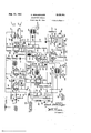
- Fig. 1 is a schematic circuit diagram of one form of the circuit utilized in the invention herein to be described.
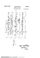
- Fig. 2 is a series of curves for the purpose of explaining the operation of the invention as exemplified by the circuit of Fig. 1.
- curve a is a schematic illustration of the R. M. A. standard form of sync signal, and is of the general type of wave fo-rmation set forth and described, for instance, on page 171 of the book published by D.
- Curve b of Fig. 2 represents the output signals from the plate circuitV of a tube to which the input signals of the form of curve a have been applied.
- vCurve c represents the Wave shape at the input of ⁇ one of the tubes later to be described.
- Curve d represents the plate current at the output of the tube to which the input signal of curve c is applied, and curve e represents the output of the horizontal discriminator, while curve f is the output signal from the vertical discriminator.
- the invention Will be seen to comprise, as diagrammatically represented, ve stages for horizontal electrostatic and vertical magnetic deflections, as well as for the sync separation and blanking, Whererthe control synchronizing inrpulses are received at a suitable input terminal in positive polarity at a certain predetermined voltage level.
- the remaining tubes of the diagrammed circuit function, as will later be set forth, for protecting the Orthicon or television scanning or camera tube in the event that either one of the deflection systems fails or has its output reduced below a cer-tain minimum safe oper'- ating level.
- the sync signals of the type illustratively represented by curve a of Fig. 2 are applied first to an input terminal ll and then fed to the sync separator tube l5 by Way of the capacity coupling element ll.
- operating voltages are applied to the tube from conductor IS, which, in tunn, derives positive voltage by way of conductors V2li and 2
- the high voltage source 22 is conventionally indicated by the battery, but it should be understood that this is merely for illustrative purposes and actually, in practice, this source may be the voltage divider resistor at the output of a filter circuit associated with an A. C. rectifier of any suitable form.
- This voltage from the source 22 energizes the plate circuit of the first half of the sync separator .tube I5 byway of the plate resistor 2l and the resistor 23 connected between the plate or anode 28 and ground 25, where the said resistors together form a voltage divider, as will later be explained.
- the tube l5 has the function of receiving signals of the type shown by curve a of Fig. 2 and, after suitably separating and clipping these signals, delivering the resulting output to the vertical and horizontal deflection units which are generally represented by the tubes 35 and 4G, respectively.
- the long frame signal Tv also represented as the second or centermost period 3H within the 9H period of curve a
- a reasonably sharp step wave front pulse such as that shown by curve d
- the pulse as shown by curve e of Fig.
- Automatic bias for the first half of the tube I5 is provided by way of the condenser and resistance combination formed of the coupling condenser I'I and the leak resistor 33, which together function under the influence of grid current resulting from the positive sync signals impressed at a predetermined voltage (for example, about volts) at the input terminal I I.
- the signals which appear in the plate circuit of the rst half of tube I5 will be of the general wave form such as those signals shown by curve b of Fig. 2. It will be seen from curve IJ of Fig. 2, that the signals, regardless of their duration, assume two precise voltage levels relative to a zero value of voltage indicated, and further, that the signals are sufficiently steep to provide a control of subsequent time-discriminator circuits.
- the output energy in the rst half of tube I5 is then fed by Way of the conductor 31 directly to control a cathode follower stage 40.
- plate Voltage is derived from the conductor I9.
- the cathode resistor 39 connected between the tube cathode and ground 25 sets a predetermined normal continuous plate current ow in the tube which is interrupted by the negative direction peaks of the signal or control wave shown by curve b of Fig. 2-
- the synchronization of the horizontal sweep oscillator is taken care of after differentiation of the interruptions in the coupling system between the two halves of the tube 40, which coupling system comprises the cathode resistors 4I for the second half of the tube and 39 for the first half of the tube and.
- the condenser and resistance combination is so calculated that when the apparent source resistance of the cathode follower stage, comprising the iii-st half of the tube 4U, is taken into account, the time constant of the differentiator circuit, including the cathode resistor 4I and the coupling condenser 43, is considerably smaller than the time duration of the slots in the vertical signal and is made of the order of one micro-second.
- the time duration of the equalizing pulses is concerned (these pulses being shown as occurring during the rst and the last periods marked 3H of the 9H control period as in Fig. 2a), the produced time constant is less than even the time duration of the equalizing pulses according to the prescribed standards which have been set up as lasting for a period of 0.04H, which substantially corresponds to 2.5 micro-seconds.
- horizontal synchronization is provided by discrimination through differentiation rather than by integration.
- vertical synchronization is provided by the circuit combination formed as the second half of the sync separator tube I5.
- the levelled output voltage from the first half of the sync separator tube I5, as it appears in conductor 31, is :fed through the high-pass filter combination comprising the capacity 41 and the resistor 49 which is grounded at 25, so that there is produced at the grid or control electrode 48 of the second half of the tube I5 an input wave of the general Wave formation exemplified by curve c of Fig. 2.
- each line synchronizing impulse is represented by a time period shown as TH 0.08H
- the time duration of the equalizing pulse is indicated by a time period TE(0.04II)
- the complete group of slotted vertical or frame synchronizing pulses is indicated by the long period Tv, which is equal to the period of three traced lines (3H) on the roster.
- the long frame signal results in a stronger positive back-kick, which is denoted by the voltage represented as ev.
- the discrimination may be simplied to the greatest extent, there exists an optimum time constant for the lter combination, comprising condenser 47 and resistor 49, which will result in a maximum voltage difference (shown'as .Ae on curve c of Fig. 2) which represents the difference between the voltage resulting from the vertical and the horizontal backkicks.
- the back-kick voltages for the horizontal and the vertical control signals may be found to Vbe in the ratio of about 1:9, so that if it is assumed, for instance, that the output wave, as in curve b of Fig.
- the back-kick of the line or horizontal synchronizing pulse will be approximately three volts while the vertical or frame back-kick voltage will be of the order of 27 volts.
- the separator tube constituting the second half of tube I5 in operation, is vgiven a suitable negative grid bias to prevent the horizontal back-kick voltage from producing any effect in the output plate current, as it appears in this half of the tube, which could disrupt or even affect the interlace of the picture.
- the blocking bias voltage applied to the second half of the separator tube I5 should amount to approximately the sum of the cut-off voltage of the second half of the tube plus the mean value of the voltage between the values represented en and ev, which, in the example of the assumed voltage range of the signal output, as in curve b of Fig. 2 and with a separator tube I5, as exemplified by the double triode type 6F8, for example, may be a bias voltage of the order of about 25 volts.
- Such a cathode bias voltage may be automatically set by the average plate current through a suitably chosen cathode resistor 5I, which will provide automatic regulation against the amplitucle variations.
- the cathode bias resistor l is shunted to ground by a suitable by-pass condenser 53 which is made large enough so that it serves to integrate the effect of the bias over a fairly substantial number of picture eld scanningvcycles, such, for example, as about 10 picture elds (one-sixth'second by present standards).
- the plate current in the output from the second half of the separator tube l5, as it appears in the output conductor 5l, is of the general wave formation exemplified illustratively by the curve d of Fig. 2.
- the plate current is of a wave formation such that it exhibits a very steep wave front which is preceded by the residual pulses S5 and S4, for instance, which result from the slots in the frame or field synchronizing signal Tv, and the signal itself has slots in it in the place of the original equalizing pulses E7 and Es, for instance, representing the seventh and eighth equalizing pulses of the group for instance.
- Ihe resulting parasitic signals are not detrimental to interlace conditions as they have double the line frequency and are of short duration, and thus, a very small energy content. However, if desired, the effects may be eliminated.
- the energizing means comprises, as aforesaid, the horizontal oscillator tube 40 operating in combination with the push-pull unit formed particularly by the second half of the amplifier unit 4F, which unit is usually and preferably combined within a single tube envelope with a driver triode first half,
- the tube 45 may, for example, be of the general type known in the art as the double triode 6F8, although it is apparent that separate tubes may be used where desired, or, in some cases,
- the horizontal oscillator system including the tube 49, is preferably of the general type shown and described in United States Patent No. 2,396,439, granted on March 12, 1946, to this same applicant upon an application which was led on March 16, 1942, as Serial No. 434,805, for an invention entitled Electron tube circuits.
- thisr combination is provided by means of the sweep condenser 6
- the first of these resistors 63 is usually made variable for frequency control purposes.
- the condenser 6l is discharged by Way of the grid current p-ulse from the triode second half of the tube 40 Which has connected thereto, in the particular form of blocking oscillator circuit described in the said co-pending application, a feed-back transformer 55, and the second half of the tube 40 is usually cut olf With the sweep condenser 6
- Synchronization control is obtained by way of the connection at the point 44 into the cathode Vcircuit of the second half of the tube 49 With the synchronizing pulses of negative polarity being applied across the cathode resistor 4 I.
- a connection of the character described provides for cooperative use with the first half of the driver triode tube 45 as a differentiator with a time constant shorter than the equalizer or slot period, as already explained, and the cathode resistor 4l also serves to limit the discharge power of the oscillator triode comprising the second half of the tube 49, i. e., to adjust the sweep amplitude. Under these circumstances, a voltage is developed across the condenser 6I which is substantially linear and of saw-tooth wave formation and which may be adjusted to a value of the order of 10% to 15% of that of the source 22 without becoming distorted.
- the voltage developed across the condenser 6I is, however, generally insufiicient of itself to drive the Orthicon deection electrode system 59, 69, or to drive directly the balanced to ground amplifier section comprising the second half of the push-pull amplifier 45. Therefore, to this end, the first half of the tube 45 provides for both voltage amplication for controlling the deflection of the scanning beam passing between the deiiecting plates 59 and r 69, and it also prevents distortion.
- the cathode element of the first half of the tube 45 has a cathode resistor 61 connecting to ground 25, so that the pre-amplifier section of tube 45 operates generally as a device of the so-called class AB type, in the manner explained in the literature.
- the Orthicon deflector system is operated in a balanced-to-ground state and, to obtain such working conditions, the second half of the tube 45 is arranged between the supply voltage source and ground, with two symmetric resistors il and V'I3 connected to the plate and cathode, respectively, for the second half of the tube 45.
- the output of the first half of the tube 45 is fed through the condenser 15 and potentiometer 16, whose other terminal connects to ground 25 through condenser Il in such a way that the control electrode 18 connects at an intermediate point on the potentiometer.
- the potentiometer will be seen also to connect into the cathode circuit of the tube through the resistor 'i9 forming a part of the cathode resistor of the tube.
- the lter combination comprising the condenser l?, which connects one end of the potentiometer 'i6 to ground and the resistor 8L' constitutes a filter which eliminates the saw-tooth component from the bias voltage applied to the control electrode 78 of the second half of the driver tube 45.
- a control of the deflection from full amplitude down to a zero deflection Value is readily obtained by an adjustment of the volume control provided through the use of the slider contact on the potentiometer l5, without changing the working point along the characteristic of tube 15.
- the Orthicon deiiector plates 55 and 56 thus connect by way of the conductors 83 and 8:3 to the plate and cathode outputs of the second half of the driver tube 45 through the blocking condensers 85 and 3S respectively.
- the remainder of the balancing arrangement comprising the balanced resistor combinations, indicated as connected between the terminal points 8l and 88 and ground 25 through the iirst and adjustable resistors, is substantially according to standard practice, and, per se, forms no part of this invention. Further detailed reference to that part of the circuit between the terminals 37 and 85 and ground 25 may be had by reference to the RCA Bulletin describing the preferred operation of the tube known in the art as the Orthicon 1840.
- the vertical deiiecting circuit includes the tube element 35 of which the second half, comprising the plate or anode electrode 89, the control electrode Si) and the cathode Qi, functions Vas a vertical oscillator tube in a manner suitable for driving or controlling the vertical amplifier tube 95.
- the circuit of the vertical oscillator comprising the second half offthe tube 35, resembles, in a substantial measure, that used for the horizontal deector circuit as embodied in the second half of tube d0.
- a resistor element 93 is connected serially relative to the sweep condenser Sri in such a manner that the resistor may be used to provide adequately for peaking.
- the filter unit comprising the condenser 9'! and the series resistor 98 serves, together with the secondary winding of the blocking transformer unit 99, to provide an oscillatory circuit with critical damping.
- this critically damped circuit comprising the transformer secondary and the series resistance and capacity network in shunt therewith, has a two-fold effeet when tuned to a frequency corresponding substantially to one line period of the deflection, as represented by the period H (see Fig. 2a).
- the duration of the recharge phase of the blocking oscillator section comprising the second half of the tube 35, is made denite and of the order of one line period and, secondly, it provides a circuit whereby the current pulse, shown by curve d of Fig. 2, as it is derived at the plate 89 of the tube 35 by way of the conductor 51 from tube l5, is such that all of the undesirable high frequency components, which might be represented by the pre-signals, such as shown at S4, S5, or the signals E7 and Ea of curve d of Fig. 2, are eliminated, so that the resulting current pulse through the transformer primary is approximately as shown and diagrammatically represented by curve f of Fig. 2.
- the plate energy voltage for the second half of tube 35 is provided through the suitable hum ltering combination comprising the resistor H95 connected in series between the conductor 2l and the plate or anode element 89, with the resistor having one terminal. shunted to ground 25 by way of the shunt condenser l'l in such a way that the resistor-condenser combination serves as a hum iilter.
- the poweramplier tube 95 derives its input energy from connection to the sweep oscillator by way of the coupling condenser 109 and the volume control unit H2, which has one terminal connected to ground 25 and which is tapped at some intermediate point H3 to provide a connection to the control electrode H5 of the power amplifier tube 95.
- This power amplier tube 95 has its cathode bias produced across cathode resistor H1.
- the sweep condenser 94 has one terminal thereof connected directly to the cathode element
- the plate or anode element I2I has connected in the circuit thereof a plate impedance element which is provided by Way of the inductance element l1
- the variable resistance in such connection may then be adjusted, as indicated, so as to make the ratio of the inductance of the winding
- the plate impedance of the power amplier tube 95 is made as large as consistent with the plate voltage drop as, in connection with the disclosed arrangement, the ratioV Y of the delector current to the plate current of the tube 95 approaches unity.
- 29 is preferably arranged to shunt the deflecting coils.
- 32 connect between the high voltage conductor 2
- 33 has one terminal thereof connected to conductor 2
- 23 connected in the plate circuit of the tube 95, is shown as constituting the primary winding of a transformer
- 36 of this transformer connects, by way of a conductor
- the camera or image scanning tube such as the Orthicon
- the protective system including the tubes
- the system is so adjusted that, in combination with a control relay
- the remaining current ow is'insuiicient to provide the control or energizati'on of the relay, with the result that, in the manner to be described, the Orthicon beam current is suppressed or blocked as soon as one or the other, or both, of the deiiection circuits fails to operate.
- the horizontal deilection voltage which was derived at the output of the second half of tube 45 and fed through the coupling condenser 85 and conductor 83, for instance, to the deflecting plate 59 is also supplied by Way of the conductor
- the vertical deiiectio energy is inductively coupled by way of thetransformer
- 40 are connected to energize the grids or control electrodes
- 50 may conveniently be in the form of a 6N7 tube, although other types of tubes may be used, or two separate triodes may be used.
- 50 assumes ⁇ a maximum value corresponding to zero grid bias which remains at substantially the same value, even under conditions where the grid control voltage across condensers
- 60 is shown as comprising a pair of coils or windings
- the relay 50 may be of any desired type, although that kno-wn in the art as the Western Electric twin coil unit has been found to be satisfactory.
- the relay has its set-up so constituted that, for energization of each of the coils
- 10 (or other suitable bias source) has its positive terminal, as indicated, connected to ground 25 and its negative terminal connected through potentiometer 1
- has its end terminals connected respectively to the negative terminal of the biasing source
- 50 has its-plate current set by adjusting the cathode resistor
- 69 permits the armature
- 83 normally is to indicate to the operator that the defiection circuits for both the horizontal deflection, as provided by the deflecting plate pair 59 and '65, and the vertical deflection, as provided by the vertical deflecting coils
- the remaining portion of the vertical oscillator tube 35 functions to control -blanking on the scanning or camera tube during the return-line, or snap-back or fly-back period of each defieotion cycle, as represented, for instance, by the time duration of the ⁇ line synchronizing pulses, as represented by the period marked TH in curve a of Fig. 2, and also the blanking period, shown by the designation 9H in Fig, 2.
- the vertical blanking period is set to continue for an additional period followingv the 9H .period of curve a of Fig. 2, which additional period varies according to desired parameters, so that the total blanking period in the vertical direction is at least 15.41-1 but not greater than 22H;
- blanking signals of this character and of a predetermined peak voltage in the positive direction are impressedL at the input terminal
- the applied blanking pulses then have their positive peaks clipped to a predetermined level by means of the grid resistor
- 13 provides the voltage for bias on the scanning or camera tube as flowing' through the resistor
- deflecting' plate pair 59 and 60 functions to produce the line: scanning which was stated to be in the hori- ⁇ Zontal direction.
- a clipper 'tube means to establish an equal amplitude level for all said received pulses
- a pair of oscillators for4 developing saw-tooth voltage waves of frequencies: closely approximating the frequencies of the dif-- ferent energy pulses
- signal separator means for separating the high frequency line and the low' frequency field energy pulses to develop line and field synchronizing control pulses, said line pulse:
- a time discriminator circuit comprising a high pass filter to couple the first said clipper tube to the said second clipper tube and a low pass filter to connect the current output of the second clipper tube into the el'd frequency oscillator, and means to control the frequency of said field frequency oscillator, a power stage connected to be energized from each oscillator to develop substantially undistorted sawtooth wave energy output for controlling the deflection of a cathode ray beam.
- a signal separating circuit for separating intermingled signal energy pulses of different time duration comprising an input clipper tube, a time discriminating network and a second clipper tube connected to receive the output signals from the time discriminating network, and means for applying an automatic bias upon second clipper tube in proportion to the average pulse current passing through the second -clipper tu-be to follow the signal strength variations of the signal energy pulses to be separated.
- a signal separating circuit for separating intermingled signal energy pulses of different time duration comprising an input clipper tube, a time discriminating network including a high pass filter and a second clipper tube connected to receive the output signals from the time discriminating network, and means for applying an automatic bias to the second clipper tube to follow the signal strength variations of the signal energy pulses to be separated.
- a signal separating circuit for separating intermingled signal energy pulses occurring at different rates comprising a rst and a second clipper tube, and a time discriminating network to couple the output of the rst clipper tube to the input of the second clipper tube, said time discriminating network having a time constant of a value intermediate the time duration of the two groups of energy pulses to be separated.
- a driving circuit for a deflection oscillator responsive to controlled signal energy impulses of predetermined time separation'and duration comprising a cathode follower triode, a differentiating network having a time constant shorter than the shortest occurring control pulse duration, and an oscillator tube connected to be controlled as to its frequency of oscillation by the ;said differentiating network, said cathode folilower triode being connected Vto energize the differentiating network and to prevent reaction Yfrom the line oscillator upon the signal source.
- a driving circuit for a relatively low frequency oscillator for controlling the deflection of a cathode ray beam which comprises a source of low frequency pulse currents, an integrating low pass filter circuit comprising at least a capacity element connected to respond to the said low frequency pulse currents, an inductive feed-back saw-tooth oscillator tube in the grid circuit of which a saw-tooth voltage wave appears, and means for connecting the pulse source of current to both the plate of the oscillator tube and the integrating network in parallel with one of the inductive feed-back elements of the oscillator, said integrating network inductive element having a time constant oscillatory period comparable to the repetition frequency of energy impulses controlling the more rapid rate of deflection.
- a defiecting circuit for deecting an electron beam within a cathode ray tube which comprises a power amplifier tube, means for establishing an automatic cathode bias on said tube, a capacitive means across which a saw-tooth voltage wave is developed, an oscillator for controlling the frequency of the saw-tooth voltage wave, and means for connecting the said capacity element in parallel with the grid cathode path of the said power amplifier.
- a deflecting circuit for deflecting an electron beam within a cathode ray tube which comprises a power ampliiier tube, means to establish an automatic cathode bias on said tube, a source of saw-tooth voltage, an oscillator for controlling the frequency of the saw-tooth voltage wave, and means for connecting the said source of sawtooth voltage in parallel with the grid and cathode path of the said power amplifier.
- a vertical deflecting circuit for a cathode ray device comprising a power amplifier tube having a control grid and a cathode, a parallel condenser and resistance combination connected between the cathode element of said tube and ground to provide grid bias on the said tube, a source of saw-tooth voltage connected between the grid and cathode of said tube, oscillator means for controlling the frequency of the developed saw-tooth voltage, and a load circuit for said tube.
Landscapes
- Engineering & Computer Science (AREA)
- Multimedia (AREA)
- Signal Processing (AREA)
- Details Of Television Scanning (AREA)
Description
Augr 12, 1947. K. scHLEsINGER 2,425,491
DEFLCTION CIRCUIT Filed June 22, 1945 2 Sheets-Sheet 1 Aug. 12,1947.
' JNVENTOR.
TTo//VEX 2 Sheets-Sheet 2 K. SCH ILESINGER` DEFLECTION CIRCUIT Filed June 22, 1943 Patented Aug. 12, 1947 DEFLECTION CIRCUIT Kurt Schlesinger, West Lafayette, 1nd,-, assignor to Radio Corporation of America, a corporation of Delaware Application June`22, 1943, Serial No. 491,759
(Cl. ri-69.5)
Claims.
This invention is directed to television circuits and apparatus. It relates primarily to control equipment and circuits for operating television camera or pick-up tubes upon which an optical image is cast and, by virtue of a scanning operation, there results a formation of wave trains of electrical video signal energy representative of the optical image.
The invention is directed, in addition, to suitable control apparatus for such a form of system wherein provision is made for the protection of the scanning or camera tube from the deleterious effects of a stationary, or substantially stationary, scanning beam which could occur in the event of a complete failure of the electron beam deflecting circuit or a substantial reduction of the scanning below a minimum level at which the scanning or camera tube can safely operate.
In its present form, the invention is particularly concerned with providing ways and means by which the television camera or scanning tube (which, for the purpose of showing one suitable example, may be considered as being of the Orthicon type) may be utilized and controlled. A tube of the general type known in the art as the Orthicon is described in an illustrative manner in the publication entitled Principles of Television Engineering, by D. G. Fink, published in 194i) by McGraw-Hill Book Company, Inc., New York, N. Y. In the publication named, the Orthicon tube is described particularly in that portion of the text between pages 111 and 116 and a schematic representation of the tube is shown on page 115. Further reference to the "Orthicon type of camera or scanning tube may be had from the various publications listed in the footnotes on page 111 of the said Fink publication.
The tube of .the type herein described as the Orthicon is one in which there is provided a mosaic electrode, which electrode usually comprises a signal plate, a dielectric member supported upon the signal plate and in which there is provided a multitude of minute photoelectric particles or globules which are carried upon the dielectric member. Mosaics of this general type are known in the art and explained in the publication above named.
In tubes of the type suggested, the electron scanning beam is directed toward the mosaic Velectrode so that it will impinge thereon Yduring .scanning at substantially all areas thereof along va path normal to the mosaic electrode member. The high speed horizontal deflection yin such a tube -is provided by apair of electrostatic deecting plates which act in combination with an axial magnetic focusing field. The slower speed vertical deiiection is accomplished by the aid of a pair of electromagnetic coils also contained within the field of the focusing coil. The result is that by virtue of the application of suitable controlled voltages to the horizontal deflecting plates, and suitable currents through the vertical deflecting coils, a low velocity electron scanning beam can 'be caused to traverse the mosaic electrode element in aline by line manner so as to neutralize or release bound charges at lthe different elemental areas of the mosaic, and more or less of the electrons of the scanning beam are absorbed or collected by the mosaic in accordance with the loss of electrons therefrom due to the brilliance of a related area of the optical image. The result of the collection of the electrons of the scanning beam upon the mosaic electrode is that a signal output kfrom the tube is provided. This signal output is-known as the train of video signal energy which can be applied across an output impedance of the camera tube through a suitable amplifier and transmission channel to recreate an optical image at monitoring or receiving points, which re-created image corresponds to the initially projected optical image that reaches the mosaic electrode of the camera tube.
The present invention is most particularly con-r cerned with the circuits by which the deflection of the scanning beam in such a device is controlled in its motion across or relative to the photoelectrically active or light sensitive mosaic electrode. 'Io this end, the presently described apparatus will be seen to include a plurality of stages for providing both the horizontal electrostatic and the vertical electromagnetic deflections and, in addition, will provide for rseparation of the sync and blanking signals from some suitable form of s ync generator which supplies the vsyn-c and blanking signals to ythe complete system. Insoiar as the protective system hereinabove described is concerned, it rcomprises essentially a rectifier arrangement or circuit which is influenced by the outgoing deflectioncurrents and voltages and, while so inuenced, causes reX- citer currents to ow through a twin coil relay which, if the sweep circuits fail or fall below a certain level, provides for an interruption of the scanning beam of the camera tube upon the cessation of the deflection in one or both of its directions of sweep. In this way, the beam current vcauses the scanning beam to be developed within the described V,type of scanning .or camera tube .and is blocked as soon vas .either one of the two sweeps fails to operate. Other features of the invention will be described in more detail from the specification to follow.
In the light of what has been stated above, it of course becomes apparent that the invention has, as one of its main objects, that of providing a control circuit for a television camera or scanning tube of the type generally known as the Orthicon At the same time, the invention has as another of its objects that of providing a circuit for protecting a television scanning or camera tube of the type described, in the event that a failure should occur in the deflecting circuit.
Other objects of the invention are those of providing a control circuit for a television scanning or camera tube which is of a simplified nature as compared to those heretofore usually known in the ant, as well as to provide a control circuit and a protective system which is highly eflicient in its use and functioning.
Still other objects of the invention are those of providing both control and protective circuits for use with television or scanning tubes where the said circuits function collectively and in their individual parts to overcome one or more of the defects of the prior art systems and yet serve to increase still further the ease of ope-ration as well as the eiiciency of operation.
Other objects and advantages will become apparent and promptly suggest themselves to those skilled in the art to which the invention is directed when the following specification is read in connection with the accompanying drawings, of which,
Fig. 1 is a schematic circuit diagram of one form of the circuit utilized in the invention herein to be described; and
Fig. 2 is a series of curves for the purpose of explaining the operation of the invention as exemplified by the circuit of Fig. 1.
In the group of curves of Fig. 2, curve a is a schematic illustration of the R. M. A. standard form of sync signal, and is of the general type of wave fo-rmation set forth and described, for instance, on page 171 of the book published by D.
G. Fink above noted. Such a form of sync sig- Y nal has also been described in [the more recent publication entitled Television Standards and Practice which was edited by the same D. G. Fink and published by the same publishers in v1943. This last named text represents certain "Selected Papers from the Proceedings of The National VTelevision System Committee and its Panels, YThe sync signal hereinabove referred to by curve a of Fig. 2 is described in the last named publication quite fully on pages 22 and 23, as well as substantially described on pages 238 and 239 of the same book.
Curve b of Fig. 2 represents the output signals from the plate circuitV of a tube to which the input signals of the form of curve a have been applied. vCurve c represents the Wave shape at the input of `one of the tubes later to be described. Curve d represents the plate current at the output of the tube to which the input signal of curve c is applied, and curve e represents the output of the horizontal discriminator, while curve f is the output signal from the vertical discriminator.
Referring now more particularly to the drawings, the invention Will be seen to comprise, as diagrammatically represented, ve stages for horizontal electrostatic and vertical magnetic deflections, as well as for the sync separation and blanking, Whererthe control synchronizing inrpulses are received at a suitable input terminal in positive polarity at a certain predetermined voltage level. The remaining tubes of the diagrammed circuit function, as will later be set forth, for protecting the Orthicon or television scanning or camera tube in the event that either one of the deflection systems fails or has its output reduced below a cer-tain minimum safe oper'- ating level. To this end, the complete system will be seen, from what is to be described, to divide itself, strictly speaking, into separate functional groups which will be seen to comprise the sync separator, the horizontal de-eotor, the vertical deflector, the protective relay system and the blanking system, all for the purpose of controlling the Orthicon or television scanning or camera tube.
The sync signals of the type illustratively represented by curve a of Fig. 2 are applied first to an input terminal ll and then fed to the sync separator tube l5 by Way of the capacity coupling element ll. In the arrangement shown, operating voltages are applied to the tube from conductor IS, which, in tunn, derives positive voltage by way of conductors V2li and 2| from a voltage source 22, having the negative terminal thereof connected to ground 25, as indicated. The high voltage source 22 is conventionally indicated by the battery, but it should be understood that this is merely for illustrative purposes and actually, in practice, this source may be the voltage divider resistor at the output of a filter circuit associated with an A. C. rectifier of any suitable form.
This voltage from the source 22 energizes the plate circuit of the first half of the sync separator .tube I5 byway of the plate resistor 2l and the resistor 23 connected between the plate or anode 28 and ground 25, where the said resistors together form a voltage divider, as will later be explained. Broadly speaking, the tube l5 has the function of receiving signals of the type shown by curve a of Fig. 2 and, after suitably separating and clipping these signals, delivering the resulting output to the vertical and horizontal deflection units which are generally represented by the tubes 35 and 4G, respectively.
In order to insure that proper inte-rlacing of the scanning or the picture takes place, it is'desirable that the long frame signal Tv, also represented as the second or centermost period 3H within the 9H period of curve a, should be such that during the period of the receipt of this signal, a reasonably sharp step wave front pulse, such as that shown by curve d, should be derived as the vertical synchronizing signal pulse. Likewise, to insure a continuous synchronization of the horizontal sweep or deflection, the pulse, as shown by curve e of Fig. 2, should be given very small inertia such as to be able .to respond during the very short period of the equalizing pulses, which (according to the above named standards) is equal to approximately O O/1H, where H is the period represented by one line of picture scanning and, for present standards, represents a time period of about 64 microseconds. Similarly the slot period existing during the vertical frame signal is equal to approximately the time period as represented in curve a, and this is equal to O OSH.V
The incoming sync signals of the characters shown by curve a of Fig. 2, when impressed upon Y the input terminal H, are to be subjected to a clipping action in the separator tube l5 at both the'positive and the negative peaks of the signais, TO this end, the series grid resistor 3|, connected to supply the signals to the grid or control electrode of the rst half of the tube I5, provides grid current clippingand the voltage divider combination in the form of resistors 28 and 27 provides plate voltage clipping by reducing substantially the plate potential on the first half of the tube.
Automatic bias for the first half of the tube I5 is provided by way of the condenser and resistance combination formed of the coupling condenser I'I and the leak resistor 33, which together function under the influence of grid current resulting from the positive sync signals impressed at a predetermined voltage (for example, about volts) at the input terminal I I.
With this result, the signals which appear in the plate circuit of the rst half of tube I5 will be of the general wave form such as those signals shown by curve b of Fig. 2. It will be seen from curve IJ of Fig. 2, that the signals, regardless of their duration, assume two precise voltage levels relative to a zero value of voltage indicated, and further, that the signals are sufficiently steep to provide a control of subsequent time-discriminator circuits.
The output energy in the rst half of tube I5 is then fed by Way of the conductor 31 directly to control a cathode follower stage 40. In this cathode follower stage, plate Voltage is derived from the conductor I9. The cathode resistor 39 connected between the tube cathode and ground 25 sets a predetermined normal continuous plate current ow in the tube which is interrupted by the negative direction peaks of the signal or control wave shown by curve b of Fig. 2- Actually, the synchronization of the horizontal sweep oscillator is taken care of after differentiation of the interruptions in the coupling system between the two halves of the tube 40, which coupling system comprises the cathode resistors 4I for the second half of the tube and 39 for the first half of the tube and. the condenser 43. In this combination, the condenser and resistance combination is so calculated that when the apparent source resistance of the cathode follower stage, comprising the iii-st half of the tube 4U, is taken into account, the time constant of the differentiator circuit, including the cathode resistor 4I and the coupling condenser 43, is considerably smaller than the time duration of the slots in the vertical signal and is made of the order of one micro-second. As far as the time duration of the equalizing pulses is concerned (these pulses being shown as occurring during the rst and the last periods marked 3H of the 9H control period as in Fig. 2a), the produced time constant is less than even the time duration of the equalizing pulses according to the prescribed standards which have been set up as lasting for a period of 0.04H, which substantially corresponds to 2.5 micro-seconds.
rIhe result is that the output signals which appear at the output terminal of the discriminator are substantially of the form shown by curve e of Fig. 2, and it will be seen that this sequence of signals continues unaltered even during the period of the frame signal, so that the horizontal synchronization takes place undisturbed during the vertical retrace period as Well as during the neld period.
A consideration of curve e of Fig. 2 will show that the negative peaks of the resulting diiferentiated pulses are always of substantially constant height or amplitude, whereas this is not true of the positive direction peaks, However, the oscillator section constituting the second half of the tube 40 responds, as it can be appreciated,v due to the cathode connection at the point 44, only to the negative peaks of the wave form shown by curve e, With the result that the varying heights of the positive peaks become immaterial.
As was explained for the horizontal synchronization in what has preceded, and as will be further amplified in what is to follow, horizontal synchronization is provided by discrimination through differentiation rather than by integration. The same is generally true of vertical synchronization, and this is provided by the circuit combination formed as the second half of the sync separator tube I5.
In this circuit embodiment, the levelled output voltage from the first half of the sync separator tube I5, as it appears in conductor 31, is :fed through the high-pass filter combination comprising the capacity 41 and the resistor 49 which is grounded at 25, so that there is produced at the grid or control electrode 48 of the second half of the tube I5 an input wave of the general Wave formation exemplified by curve c of Fig. 2.
In the diagram of Fig. 2, and particularly curve a, it will be seen that the duration of each line synchronizing impulse is represented by a time period shown as TH 0.08H), and that the time duration of the equalizing pulse is indicated by a time period TE(0.04II) and that the complete group of slotted vertical or frame synchronizing pulses is indicated by the long period Tv, which is equal to the period of three traced lines (3H) on the roster. The long frame signal, however, results in a stronger positive back-kick, which is denoted by the voltage represented as ev.
In order that the discrimination may be simplied to the greatest extent, there exists an optimum time constant for the lter combination, comprising condenser 47 and resistor 49, which will result in a maximum voltage difference (shown'as .Ae on curve c of Fig. 2) which represents the difference between the voltage resulting from the vertical and the horizontal backkicks. By suitable choice of circuit parameters, the back-kick voltages for the horizontal and the vertical control signals may be found to Vbe in the ratio of about 1:9, so that if it is assumed, for instance, that the output wave, as in curve b of Fig. 2, appearing at the plate of the rst half of separator tube I5, is of the order of 30 volts amplitude, the back-kick of the line or horizontal synchronizing pulse will be approximately three volts while the vertical or frame back-kick voltage will be of the order of 27 volts.
To this end, the separator tube constituting the second half of tube I5, in operation, is vgiven a suitable negative grid bias to prevent the horizontal back-kick voltage from producing any effect in the output plate current, as it appears in this half of the tube, which could disrupt or even affect the interlace of the picture. In other Words, the blocking bias voltage applied to the second half of the separator tube I5 should amount to approximately the sum of the cut-off voltage of the second half of the tube plus the mean value of the voltage between the values represented en and ev, which, in the example of the assumed voltage range of the signal output, as in curve b of Fig. 2 and with a separator tube I5, as exemplified by the double triode type 6F8, for example, may be a bias voltage of the order of about 25 volts.
Such a cathode bias voltage may be automatically set by the average plate current through a suitably chosen cathode resistor 5I, which will provide automatic regulation against the amplitucle variations. The cathode bias resistor l is shunted to ground by a suitable by-pass condenser 53 which is made large enough so that it serves to integrate the effect of the bias over a fairly substantial number of picture eld scanningvcycles, such, for example, as about 10 picture elds (one-sixth'second by present standards).
Under these circumstances, the plate current in the output from the second half of the separator tube l5, as it appears in the output conductor 5l, is of the general wave formation exemplified illustratively by the curve d of Fig. 2. In this curve, it will be seen that the plate current is of a wave formation such that it exhibits a very steep wave front which is preceded by the residual pulses S5 and S4, for instance, which result from the slots in the frame or field synchronizing signal Tv, and the signal itself has slots in it in the place of the original equalizing pulses E7 and Es, for instance, representing the seventh and eighth equalizing pulses of the group for instance. Ihe resulting parasitic signals are not detrimental to interlace conditions as they have double the line frequency and are of short duration, and thus, a very small energy content. However, if desired, the effects may be eliminated.
completely from the vertical sync quite readily by the aid of an integrating or selector device of the general character which will be discussed later in connection with the vertical deflection.
At this point it might be pointed out that the use of such integrators subsequent to separation by differentiation, as above explained, can be made to maintain the advantages of that method to define the vertical firing or triggering point of the vertical Sweep or deilection with somewhat greater precision due to the steeper wave front than the more conventionally used method of direct integration of the frame or field signal.
It was explained, in the foregoing portion of this disclosure, that in the Orthicon tube, which is assumed herein, by way of example, to be the.
type of scanning or camera tubeto which the described arrangement is particularly adapted, the rapid or horizontal deflection of the scanning beam, in its traversal of the mosaic electrode, took place under the control of electrostatic deecting plates or electrode members. Such plate or electrode systems are conventionally represented herein as embodying the deilecto-r plates 59 and B6.
To control these deecting plates and to produce the voltages applied thereto, the energizing means comprises, as aforesaid, the horizontal oscillator tube 40 operating in combination with the push-pull unit formed particularly by the second half of the amplifier unit 4F, which unit is usually and preferably combined within a single tube envelope with a driver triode first half,
so that the tube 45 may, for example, be of the general type known in the art as the double triode 6F8, although it is apparent that separate tubes may be used where desired, or, in some cases,
that tubes having slightly different characteristics may be substituted.
The horizontal oscillator system, including the tube 49, is preferably of the general type shown and described in United States Patent No. 2,396,439, granted on March 12, 1946, to this same applicant upon an application which was led on March 16, 1942, as Serial No. 434,805, for an invention entitled Electron tube circuits. Generally speaking, thisr combination is provided by means of the sweep condenser 6|, which is charged from the voltage source 22 through the resistors 63 and 64 which connect to conductor I9. The first of these resistors 63 is usually made variable for frequency control purposes. The condenser 6l is discharged by Way of the grid current p-ulse from the triode second half of the tube 40 Which has connected thereto, in the particular form of blocking oscillator circuit described in the said co-pending application, a feed-back transformer 55, and the second half of the tube 40 is usually cut olf With the sweep condenser 6| charged strongly negative.
Synchronization control is obtained by way of the connection at the point 44 into the cathode Vcircuit of the second half of the tube 49 With the synchronizing pulses of negative polarity being applied across the cathode resistor 4 I. A connection of the character described provides for cooperative use with the first half of the driver triode tube 45 as a differentiator with a time constant shorter than the equalizer or slot period, as already explained, and the cathode resistor 4l also serves to limit the discharge power of the oscillator triode comprising the second half of the tube 49, i. e., to adjust the sweep amplitude. Under these circumstances, a voltage is developed across the condenser 6I which is substantially linear and of saw-tooth wave formation and which may be adjusted to a value of the order of 10% to 15% of that of the source 22 without becoming distorted.
The voltage developed across the condenser 6I is, however, generally insufiicient of itself to drive the Orthicon deection electrode system 59, 69, or to drive directly the balanced to ground amplifier section comprising the second half of the push-pull amplifier 45. Therefore, to this end, the first half of the tube 45 provides for both voltage amplication for controlling the deflection of the scanning beam passing between the deiiecting plates 59 and r 69, and it also prevents distortion. To this end, the cathode element of the first half of the tube 45 has a cathode resistor 61 connecting to ground 25, so that the pre-amplifier section of tube 45 operates generally as a device of the so-called class AB type, in the manner explained in the literature. For instance, this "class AB type of tube operation is described in the book Ultra-high Frequency Techniques, by Brainerd, Koehler, Reich and Woodruff, published in 1942 by D. Van Nostrand Co., Inc., of New York, N. Y., to which text reference-is made, and particularly to page 77, etc., thereof. In this way, the non-linearity of the tube characteristic at the chosen point is of just the sense and the proper magnitude to compensate for any saw-tooth distortion of the input which may occur if the voltage across the condenser element 6I is adjusted for fairly large amplitudes. Accordingly, with this operation, as described, there is developed across the load re sistor 69 of the rst half of tube 45, a linearly corrected saw-tooth voltage wave to control the operation of the Ortl-iicon deflection.
To provide for this form of operation, the Orthicon deflector system is operated in a balanced-to-ground state and, to obtain such working conditions, the second half of the tube 45 is arranged between the supply voltage source and ground, with two symmetric resistors il and V'I3 connected to the plate and cathode, respectively, for the second half of the tube 45. In order that sweep amplitude of the resulting deflection may -be adjusted, the output of the first half of the tube 45 is fed through the condenser 15 and potentiometer 16, whose other terminal connects to ground 25 through condenser Il in such a way that the control electrode 18 connects at an intermediate point on the potentiometer. The potentiometer will be seen also to connect into the cathode circuit of the tube through the resistor 'i9 forming a part of the cathode resistor of the tube.
The lter combination comprising the condenser l?, which connects one end of the potentiometer 'i6 to ground and the resistor 8L' constitutes a filter which eliminates the saw-tooth component from the bias voltage applied to the control electrode 78 of the second half of the driver tube 45. In this way, a control of the deflection from full amplitude down to a zero deflection Value is readily obtained by an adjustment of the volume control provided through the use of the slider contact on the potentiometer l5, without changing the working point along the characteristic of tube 15.
The Orthicon deiiector plates 55 and 56 thus connect by way of the conductors 83 and 8:3 to the plate and cathode outputs of the second half of the driver tube 45 through the blocking condensers 85 and 3S respectively. The remainder of the balancing arrangement comprising the balanced resistor combinations, indicated as connected between the terminal points 8l and 88 and ground 25 through the iirst and adjustable resistors, is substantially according to standard practice, and, per se, forms no part of this invention. Further detailed reference to that part of the circuit between the terminals 37 and 85 and ground 25 may be had by reference to the RCA Bulletin describing the preferred operation of the tube known in the art as the Orthicon 1840.
The vertical deiiecting circuit includes the tube element 35 of which the second half, comprising the plate or anode electrode 89, the control electrode Si) and the cathode Qi, functions Vas a vertical oscillator tube in a manner suitable for driving or controlling the vertical amplifier tube 95. Generally speaking, the circuit of the vertical oscillator, comprising the second half offthe tube 35, resembles, in a substantial measure, that used for the horizontal deector circuit as embodied in the second half of tube d0. However, in the arrangement shown, in contrast to what is shown for the horizontal oscillator, a resistor element 93 is connected serially relative to the sweep condenser Sri in such a manner that the resistor may be used to provide adequately for peaking.
In conjunction with the vertical oscillator, the filter unit comprising the condenser 9'! and the series resistor 98 serves, together with the secondary winding of the blocking transformer unit 99, to provide an oscillatory circuit with critical damping. Generally speaking, this critically damped circuit, comprising the transformer secondary and the series resistance and capacity network in shunt therewith, has a two-fold effeet when tuned to a frequency corresponding substantially to one line period of the deflection, as represented by the period H (see Fig. 2a). These eifects are that the duration of the recharge phase of the blocking oscillator section, comprising the second half of the tube 35, is made denite and of the order of one line period and, secondly, it provides a circuit whereby the current pulse, shown by curve d of Fig. 2, as it is derived at the plate 89 of the tube 35 by way of the conductor 51 from tube l5, is such that all of the undesirable high frequency components, which might be represented by the pre-signals, such as shown at S4, S5, or the signals E7 and Ea of curve d of Fig. 2, are eliminated, so that the resulting current pulse through the transformer primary is approximately as shown and diagrammatically represented by curve f of Fig. 2. It thus becomes apparent that the vertical synchronization, as it aects the system herein set forth, will be caused to occur at the end of the frame or field period represented by Tv, for instance, by curve a of Fig. 2. Suitable interlacing results from tuning the plate coil once for all, and thereafter, synchronization is so stable that any Variations of the frequency control resistor IGI, of the resistor pair IUI and |02, which charges the sweep condenser 94 through the pealdng resistor 93, change the amplitude of the sweep rather than the sweep frequency.
To stabilize still further the operation of the system, the plate energy voltage for the second half of tube 35, like the second half of tube l5, is provided through the suitable hum ltering combination comprising the resistor H95 connected in series between the conductor 2l and the plate or anode element 89, with the resistor having one terminal. shunted to ground 25 by way of the shunt condenser l'l in such a way that the resistor-condenser combination serves as a hum iilter.
The poweramplier tube 95 derives its input energy from connection to the sweep oscillator by way of the coupling condenser 109 and the volume control unit H2, which has one terminal connected to ground 25 and which is tapped at some intermediate point H3 to provide a connection to the control electrode H5 of the power amplifier tube 95. This power amplier tube 95 has its cathode bias produced across cathode resistor H1. l
Norma1ly, some diiiiculty in Vertical amplification would tend to be introduced by negative feed-back produced across the cathode bias resistor H1, which cannot be readily by-passed to ground 25 at the low frequencies involved for the Vertical deflection. To this end, and in order to avoid an unusually large by-pass condenser H9 shunting the cathode bias resistor Il'l in order to prevent cathode degeneration which has a tendency Yto cause a loss in low frequency components and thus bring about distortion, the sweep condenser 94 has one terminal thereof connected directly to the cathode element |29 of the. vpower amplier 95. This connection, rather than the usualV connection directly to ground 2.5, asis provided for instance for the horizontal sweep condenser 6l, avoids distortion,
as will be described. The result of the connection shownrelative to the vertical sweep condenser 94. and the cathode of the power amplier 95 is that the degenerative voltage drops, which are inherently produced across the cathode bias resistor l l1, do not subtract from the cathode to grid voltage but rather subtract from the plate to ground voltage Where no detrimental' effects result. In fact, improved sawtooth linearity is achieved even though the condenser l|l9 is made but a minor fraction of the size normally to be expected in order to prevent thedetrimental effects of cathode degeneration.
Iny connection with the power amplifier 95, the plate or anode element I2I has connected in the circuit thereof a plate impedance element which is provided by Way of the inductance element l1 |23, serially connected with the variable resistor |24 through which plate voltage to the tube 95 is supplied. The variable resistance in such connection may then be adjusted, as indicated, so as to make the ratio of the inductance of the winding |23 to the resistance of the resistor |24 in the plate circuit of the tube 95 equal to the corresponding time constant of the vertical dflector coils for the tube, which coils are conventionally represented by the windings `|25 and |25. To this end, the plate impedance of the power amplier tube 95 is made as large as consistent with the plate voltage drop as, in connection with the disclosed arrangement, the ratioV Y of the delector current to the plate current of the tube 95 approaches unity.
In order that there may be no over-shoot and, at the same time, to provide for a smooth ilyback or return-trace of the scanning beam during the rapid portion of the saw-tooth, a tuning condenser |29 is preferably arranged to shunt the deflecting coils.
So that the scanning beam within the scanning or camera tube may be positioned vertically, various bleeder resistors |30, |3| and |32 connect between the high voltage conductor 2| and ground 2-5. The blocking condenser |33 has one terminal thereof connected to conductor 2| and the other terminal thereof tapped to one of the bleeder resistors |3|.
It will be noted that the inductance |23, connected in the plate circuit of the tube 95, is shown as constituting the primary winding of a transformer |35. The secondary Winding |36 of this transformer connects, by way of a conductor |31, to control the protective relay system comprising the tubes |40 and |50 and their associated circuit elements.
In any installation of the character hereinabove described, it is, as hereinabove noted, particularly desirable that the camera or image scanning tube, such as the Orthicon, be protected against any failure of the deilecting circuits in order to prevent any possible damage to -the camera tube signal plate (or mosaic) in the event of a failure of any part of the deiiecting system, where a stationary or substantially stationary impacting electron beam would cause damage. To this end, the protective system, including the tubes |40 and |50, is so designed and constituted that currents cease to flow therethrough as soon as either the horizontal or the vertical sweep circuit falls below a certain predetermined output level'. The system is so adjusted that, in combination with a control relay |60, the simultaneous ow of current, due to both the horizonta1 and vertical deflection energy, serves to trigger or operate the relay. However, if one of the deflection circuits fails, the remaining current ow is'insuiicient to provide the control or energizati'on of the relay, with the result that, in the manner to be described, the Orthicon beam current is suppressed or blocked as soon as one or the other, or both, of the deiiection circuits fails to operate.
The horizontal deilection voltage which was derived at the output of the second half of tube 45 and fed through the coupling condenser 85 and conductor 83, for instance, to the deflecting plate 59 is also supplied by Way of the conductor |4| and the coupling condenser |43 across the resistor |44 to the plate element |45 of the double diode tube |40, Vwhich tube, for instance, though not necessarily, may be of the general type known in the art as the rIAG.
As was above indicated, the vertical deiiectio energy is inductively coupled by way of thetransformer |35 and its'secondary winding |36 to be supplied by the conductor |31V to the second plate or anode |41 of the double diode |40. Itthus can be seen that both cathode elements |48 and |49 of the double diode |40 develop positive voltages relative to ground 25 across the condensers |'5| and |52, respectively, of which the condenser |52 is larger than |5|. These condensers are shunted by suitable resistor elements |54 and |55, and the time constants of the combinations are preferably adjusted to .be of the order of approXimately one second, which, obviously, determines the speed of response of the protective system.
The rectified voltages which appear in the output of the double diode tube |40 are connected to energize the grids or control electrodes |56 and |51 of the twin triode tube |50 through the series resistor elements |58 and |59, respectively. The twin triode tube |50 may conveniently be in the form of a 6N7 tube, although other types of tubes may be used, or two separate triodes may be used.
With the connection shown, the plate current flow in the twin triode |50 assumes `a maximum value corresponding to zero grid bias which remains at substantially the same value, even under conditions where the grid control voltage across condensers |5| and |52 further increases toward a maximum predetermined voltage value` The control relay element |60 is shown as comprising a pair of coils or windings |6| and |62 which are connected to be energized in accordance with the plate current flowing through each half of the twin triode tube 50, in that the plate or anode electrodes |63 and |64 of this tube receive operating voltage from the voltage source 22 by way of the conductors 2| and |65, respectively. The relay 50 may be of any desired type, although that kno-wn in the art as the Western Electric twin coil unit has been found to be satisfactory. The relay has its set-up so constituted that, for energization of each of the coils |6| and |62, the armatures |66 and |61 are so controlled that the armature |66 closes upon its contact point |68 while the armature |61 is Withdrawn from its contact point |69.
The bias battery |10 (or other suitable bias source) has its positive terminal, as indicated, connected to ground 25 and its negative terminal connected through potentiometer 1| and the tapping point |13 and thence co-nductor |15 and resistor |16 to the terminal point |80, to which terminal point the grid or control electrode (not shown) of the Orthicon image scanning or camera tube is connected.
It can Vbe seen, from the connection indicated, that the potentiometer |1| has its end terminals connected respectively to the negative terminal of the biasing source |10 and the positive terminal of the plate voltage source 22, so that now if the cathode resistor |11 of the twin triode |50 is set for a predetermined current flow through the tube, it can be appreciated that any `change in the current flow permitting the armature |61 to close upon contact |69, due to a reduction of the current flowing through the Winding |62, will promptly provide a short circuit of that portion of the potentiometer |1| between the point |13 and the negative terminal of the bias source |10, so that negative Voltage of the Isource |10 becomes effective at the grid or control electrode of the camera or scanning tube,
'which electrodeconnects, as above stated, at the terminal point |89. v v
In the preferred circuit arrangement, the tube |50 has its-plate current set by adjusting the cathode resistor |11 to a predetermined value for producing a predetermined minimum current in the event the rectifier hinput fails. At this current iiow the relay 599 will be de-energized, in that there is not sufficient current flowing through the tube |59 to actuate it. Y
Accordingly, under such conditions, with the action as above expressed and the relay |69 deenergized, tlie relay armature |61 engages the contact point |69, so that a blocking or cut-olf bias` is supplied from the source |19 to the scanning tube. Attlie same time, the de-energization of the relay |69 permits the armature |66 to Aassume a position remote from the contact point |687l so that a circuit through the indicator lamp |83, which, in an energized state of the relay, had been lit by virtue of current flowing from the sou'rce |9|, is broken, The illumination of the pilot lamp |83 normally is to indicate to the operator that the defiection circuits for both the horizontal deflection, as provided by the deflecting plate pair 59 and '65, and the vertical deflection, as provided by the vertical deflecting coils |25 and |26, is in a state of normal and satisfactory operation.
The remaining portion of the vertical oscillator tube 35, that is, the rst half of thetube, functions to control -blanking on the scanning or camera tube during the return-line, or snap-back or fly-back period of each defieotion cycle, as represented, for instance, by the time duration of the` line synchronizing pulses, as represented by the period marked TH in curve a of Fig. 2, and also the blanking period, shown by the designation 9H in Fig, 2. However, Where presently accepted standards', as recommended by the R. M. A. and the Federal Communications Commission, are adopted, the vertical blanking period is set to continue for an additional period followingv the 9H .period of curve a of Fig. 2, which additional period varies according to desired parameters, so that the total blanking period in the vertical direction is at least 15.41-1 but not greater than 22H;
Signals for controlling blanking during the stated `period are likewise producedY according to prescribed standards, and suitable blanking signals'` are represented in the Fink publication, above cited, particularly by the diagrammatic illustrations on pages 168, 170, 171 and 399 of the said book. Also, blanking signals of the character desired for providing the blanking effect have been describ-ed in one form of their production in applicants co-pending application, Serial No. 452,921, led July 30, 1942, which is now issued as United States Patent No. 2,366,536, granted lJune` 2,1945, and also by applicants co-pending application, Serial l\To 485,982, f-lled May 7, 1913, and now issued asAUnited States Patent No. 2,3676,358,gr anted June 2, 1945.
Thus, blanking signals of this character and of a predetermined peak voltage in the positive direction are impressedL at the input terminal |99 and fed through the coupling condenser 19| so as to set up, by reason of the positive peak values thereof, an automatic bias for the first half of the tube 35 across the resistor |92, The applied blanking pulses then have their positive peaks clipped to a predetermined level by means of the grid resistor |93 which is in series with the coupling condenser |91 and connects to the grid or control electrode |94 of the first half of the tube 95. It thus becomes evident' that relatively strong negative blanking impulses will appear at the` plate or anode electrode |95 of the tubel 35, in that the cathode element |95 connects directly to ground |25 and no degeneration takes place;
Accordingly, these strong negative blanking impulses, lclue to amplification in the nrst half'lof tube 35, are supplied by way of the condensers. |99 and |91 to the output terminal |80, wherefrom they are supplied to the grid or control-electrode of the scanning or camera tube (not shown)I along with the bias voltages.
It will be noted that the volume control ar rangement provided by the potentiometer 11|,` and its tapping point |13, provides the voltage for bias on the scanning or camera tube as flowing' through the resistor |16 which forms one part of` the load impedance of the first half of the tube 35, but Whenever the relay coil |62 of the relay |69 becomes de-energized, by reason of a reduction in current fiow in the tube |50, the complete blocking voltage of the bias source |19 is appliedl also at the terminalpoint |89, since the closure` of the armature |61 on contact |69 short circuits'.
a part of potentiometer |1| and makes the volt-v age of the source |19 effective as a negative bias: at the output terminal.
It has been above suggested that the deflecting' plate pair 59 and 60 functions to produce the line: scanning which was stated to be in the hori-` Zontal direction.
in the vertical direction. u
It is, of course, to be understood that these ref-- erences are merely illustrative and, if it is desired to have the line scanning in the vertical div rection and the eld or frame scanning in the lat-` eral direction, that is, each normal to the presently accepted directions, the system herein dis-v Closed Will functionv equally as Well When it isfy borne in mind that the 'deecting plate pair 59 and 69 functions to produce the rapid scanning'. and the defiecting coils |25 and |26 function to` produce the slower field or frame scanning and"A are each, broadly speaking, independent of limi-- tations as to Whether they occur in the verticali or the horizontal directions.
Many modifications ofthe described arrange ment Will, of course, be possible, and it is to be:- understood that Within the scope of the disclosure.l many and various modifications may be utilized..
Having now described the invention, what is; claimed is:
1. In a deflection circuit for television apparatus responsive to a signal energy received from' a source Whereat intermingled energy pulses of. different time 'duration for relatively high fre-4 quency line and relatively low frequency field de flection control are developed, a clipper 'tube means to establish an equal amplitude level for all said received pulses, a pair of oscillators for4 developing saw-tooth voltage waves of frequencies: closely approximating the frequencies of the dif-- ferent energy pulses, signal separator means for separating the high frequency line and the low' frequency field energy pulses to develop line and field synchronizing control pulses, said line pulse:
separating means including a, high pass filter andi a coupling tube for energizing said filter, and'. means to control the frequency of the oscillator developing output energy at substantially the linefrequency from the output of the high pass filter, said field pulse separating means including a sec- It Was also stated that theiv deflecting coils |25 and |26 would producethe-Y eld or frame scanning which was stated to be.`-
ond clipper tube, a time discriminator circuit comprising a high pass filter to couple the first said clipper tube to the said second clipper tube and a low pass filter to connect the current output of the second clipper tube into the el'd frequency oscillator, and means to control the frequency of said field frequency oscillator, a power stage connected to be energized from each oscillator to develop substantially undistorted sawtooth wave energy output for controlling the deflection of a cathode ray beam.
2. A signal separating circuit for separating intermingled signal energy pulses of different time duration comprising an input clipper tube, a time discriminating network and a second clipper tube connected to receive the output signals from the time discriminating network, and means for applying an automatic bias upon second clipper tube in proportion to the average pulse current passing through the second -clipper tu-be to follow the signal strength variations of the signal energy pulses to be separated.
3. A signal separating circuit for separating intermingled signal energy pulses of different time duration comprising an input clipper tube, a time discriminating network including a high pass filter and a second clipper tube connected to receive the output signals from the time discriminating network, and means for applying an automatic bias to the second clipper tube to follow the signal strength variations of the signal energy pulses to be separated.
4. A signal separating circuit for separating intermingled signal energy pulses occurring at different rates comprising a rst and a second clipper tube, and a time discriminating network to couple the output of the rst clipper tube to the input of the second clipper tube, said time discriminating network having a time constant of a value intermediate the time duration of the two groups of energy pulses to be separated.
5. A driving circuit for a deflection oscillator responsive to controlled signal energy impulses of predetermined time separation'and duration comprising a cathode follower triode, a differentiating network having a time constant shorter than the shortest occurring control pulse duration, and an oscillator tube connected to be controlled as to its frequency of oscillation by the ;said differentiating network, said cathode folilower triode being connected Vto energize the differentiating network and to prevent reaction Yfrom the line oscillator upon the signal source.
6. A driving circuit for a relatively low frequency =osci1lator for controlling the deflection of a cath- ,ode ray beam which comprises a source of low- ',irequency pulse currents, an integrating low pass lter circuit comprising capacity and resistance elements connected to respond to the said lowfrequency pulse currents, an inductive feed-back saw-tooth oscillator tube in the grid circuit of which a saw-tooth voltage wave appears, and means for connecting the pulse source of current to both the plate of the oscillator tube and the integrating network in parallel with one of the inductive feed-back elements of the oscillator,
said integrating network inductive element having a time constant oscillatory period comparable to the repetition frequency of energy impulses controlling the more rapid rate of deflection. 5 '7. A driving circuit for a relatively low frequency oscillator for controlling the deflection of a cathode ray beam which comprises a source of low frequency pulse currents, an integrating low pass filter circuit comprising at least a capacity element connected to respond to the said low frequency pulse currents, an inductive feed-back saw-tooth oscillator tube in the grid circuit of which a saw-tooth voltage wave appears, and means for connecting the pulse source of current to both the plate of the oscillator tube and the integrating network in parallel with one of the inductive feed-back elements of the oscillator, said integrating network inductive element having a time constant oscillatory period comparable to the repetition frequency of energy impulses controlling the more rapid rate of deflection.
8. A defiecting circuit for deecting an electron beam within a cathode ray tube which comprises a power amplifier tube, means for establishing an automatic cathode bias on said tube, a capacitive means across which a saw-tooth voltage wave is developed, an oscillator for controlling the frequency of the saw-tooth voltage wave, and means for connecting the said capacity element in parallel with the grid cathode path of the said power amplifier.
9. A deflecting circuit for deflecting an electron beam within a cathode ray tube which comprises a power ampliiier tube, means to establish an automatic cathode bias on said tube, a source of saw-tooth voltage, an oscillator for controlling the frequency of the saw-tooth voltage wave, and means for connecting the said source of sawtooth voltage in parallel with the grid and cathode path of the said power amplifier.
l0. A vertical deflecting circuit for a cathode ray device comprising a power amplifier tube having a control grid and a cathode, a parallel condenser and resistance combination connected between the cathode element of said tube and ground to provide grid bias on the said tube, a source of saw-tooth voltage connected between the grid and cathode of said tube, oscillator means for controlling the frequency of the developed saw-tooth voltage, and a load circuit for said tube.
KURT SCI-ILESINGER.
REFERENCES CITED Number 6o 2,096,877
Date
2,261,645 Delvaux Nov. 4, 1941 2,261,776 Poeh Nov. 4, 1941 2,310,888 Banring et ai Feb. 9, 1943 2,297,742 Campbell oct. e, 1942 2,299,361 Tolson Oct. 20, 1942 Disclaimer 2,425,49L`Kwt Sohlesmger, West Lafayette, Ind. DEFLECTION CIRCUIT. Patent dated Aug. 12, 1947. Disclaimer filed June 22, 1950, by the assignee, Radio Corporation of America. Hereby enters this disclaimer to claims 8, 9, and 10 of said patent. [Qjical Gazette July 25, 1950] yet te, Ind. DEFLECTION CIRCUIT. Patent dated ug. 12, 1947. isclaimer filed June 22, 1950, by the assignee, Radio Oorporation of America.
Hereby enters this disclaimer to claims 8, 9, and 10 of said patent.
[Oficial Gazette July 25, 1950]
Priority Applications (1)
| Application Number | Priority Date | Filing Date | Title |
|---|---|---|---|
| US491759A US2425491A (en) | 1943-06-22 | 1943-06-22 | Deflection circuit |
Applications Claiming Priority (1)
| Application Number | Priority Date | Filing Date | Title |
|---|---|---|---|
| US491759A US2425491A (en) | 1943-06-22 | 1943-06-22 | Deflection circuit |
Publications (1)
| Publication Number | Publication Date |
|---|---|
| US2425491A true US2425491A (en) | 1947-08-12 |
Family
ID=23953542
Family Applications (1)
| Application Number | Title | Priority Date | Filing Date |
|---|---|---|---|
| US491759A Expired - Lifetime US2425491A (en) | 1943-06-22 | 1943-06-22 | Deflection circuit |
Country Status (1)
| Country | Link |
|---|---|
| US (1) | US2425491A (en) |
Cited By (7)
| Publication number | Priority date | Publication date | Assignee | Title |
|---|---|---|---|---|
| US2508923A (en) * | 1946-06-27 | 1950-05-23 | Rca Corp | Synchronizing system |
| US2577848A (en) * | 1950-02-16 | 1951-12-11 | Rca Corp | Protective circuit |
| US2582014A (en) * | 1948-05-08 | 1952-01-08 | Radio Ind S A Soc | Scanning device for television transmitters |
| US2597092A (en) * | 1946-09-19 | 1952-05-20 | Motorola Inc | Vertical sweep generator |
| US2616976A (en) * | 1947-03-05 | 1952-11-04 | Hartford Nat Bank & Trust Co | Multiplex radio receiver |
| US2652450A (en) * | 1948-05-29 | 1953-09-15 | Rca Corp | Sync separation and automatic gain control |
| US2713611A (en) * | 1952-03-01 | 1955-07-19 | Motorola Inc | Television circuit |
Citations (6)
| Publication number | Priority date | Publication date | Assignee | Title |
|---|---|---|---|---|
| US2096877A (en) * | 1933-11-03 | 1937-10-26 | Emi Ltd | Television and like system |
| US2261645A (en) * | 1939-05-11 | 1941-11-04 | Gen Electric | Protective system |
| US2261776A (en) * | 1938-12-30 | 1941-11-04 | Rca Corp | Cathode ray tube apparatus |
| US2297742A (en) * | 1941-07-15 | 1942-10-06 | Du Mont Allen B Lab Inc | Blocking tube oscillator for television |
| US2299361A (en) * | 1939-12-29 | 1942-10-20 | Rca Corp | Television system |
| US2310888A (en) * | 1940-03-14 | 1943-02-09 | Bahring Herbert | Synchronized saw-tooth current generator |
-
1943
- 1943-06-22 US US491759A patent/US2425491A/en not_active Expired - Lifetime
Patent Citations (6)
| Publication number | Priority date | Publication date | Assignee | Title |
|---|---|---|---|---|
| US2096877A (en) * | 1933-11-03 | 1937-10-26 | Emi Ltd | Television and like system |
| US2261776A (en) * | 1938-12-30 | 1941-11-04 | Rca Corp | Cathode ray tube apparatus |
| US2261645A (en) * | 1939-05-11 | 1941-11-04 | Gen Electric | Protective system |
| US2299361A (en) * | 1939-12-29 | 1942-10-20 | Rca Corp | Television system |
| US2310888A (en) * | 1940-03-14 | 1943-02-09 | Bahring Herbert | Synchronized saw-tooth current generator |
| US2297742A (en) * | 1941-07-15 | 1942-10-06 | Du Mont Allen B Lab Inc | Blocking tube oscillator for television |
Cited By (7)
| Publication number | Priority date | Publication date | Assignee | Title |
|---|---|---|---|---|
| US2508923A (en) * | 1946-06-27 | 1950-05-23 | Rca Corp | Synchronizing system |
| US2597092A (en) * | 1946-09-19 | 1952-05-20 | Motorola Inc | Vertical sweep generator |
| US2616976A (en) * | 1947-03-05 | 1952-11-04 | Hartford Nat Bank & Trust Co | Multiplex radio receiver |
| US2582014A (en) * | 1948-05-08 | 1952-01-08 | Radio Ind S A Soc | Scanning device for television transmitters |
| US2652450A (en) * | 1948-05-29 | 1953-09-15 | Rca Corp | Sync separation and automatic gain control |
| US2577848A (en) * | 1950-02-16 | 1951-12-11 | Rca Corp | Protective circuit |
| US2713611A (en) * | 1952-03-01 | 1955-07-19 | Motorola Inc | Television circuit |
Similar Documents
| Publication | Publication Date | Title |
|---|---|---|
| US2431824A (en) | Automatic volume control regulation of light intensity on camera tube | |
| US2425491A (en) | Deflection circuit | |
| US2261776A (en) | Cathode ray tube apparatus | |
| US2227197A (en) | Signaling system | |
| US2801364A (en) | Circuit-arrangement in which a signal is supplied to a control-device | |
| US2240281A (en) | Automatic background control | |
| US2296393A (en) | Noise limiter | |
| US2543719A (en) | Deflection circuit | |
| US2810825A (en) | Automatic gain control means | |
| US2207775A (en) | Television receiver | |
| US2229964A (en) | Television synchronizing system | |
| US2052184A (en) | Electric wave generator | |
| GB1069597A (en) | Improvements in or relating to television camera tube systems | |
| US2256529A (en) | Synchronizing signal separator circuit | |
| US2363822A (en) | Saw-tooth deflection | |
| US2178758A (en) | Television system | |
| US2305902A (en) | Television transmission | |
| US2289948A (en) | Video-frequency signal-translating system for television receivers | |
| US2236066A (en) | Television apparatus | |
| US2543304A (en) | Circuit for maintaining aspect ratio constant | |
| US2207389A (en) | Cathode ray tube deflecting circuit | |
| US3294904A (en) | Keyed a. g. c. with variable reactance for control of keying pulse amplitude | |
| US2505367A (en) | Television receiver brightness and contrast control | |
| US3005870A (en) | Television receiver | |
| US2885473A (en) | Non-blocking wave receiver circuit with automatic gain control |