US20240297193A1 - Image sensor and method for forming the same - Google Patents
Image sensor and method for forming the same Download PDFInfo
- Publication number
- US20240297193A1 US20240297193A1 US18/176,854 US202318176854A US2024297193A1 US 20240297193 A1 US20240297193 A1 US 20240297193A1 US 202318176854 A US202318176854 A US 202318176854A US 2024297193 A1 US2024297193 A1 US 2024297193A1
- Authority
- US
- United States
- Prior art keywords
- image sensor
- forming
- layer
- isolation
- isolation structure
- Prior art date
- Legal status (The legal status is an assumption and is not a legal conclusion. Google has not performed a legal analysis and makes no representation as to the accuracy of the status listed.)
- Pending
Links
Images


Classifications
-
- H—ELECTRICITY
- H10—SEMICONDUCTOR DEVICES; ELECTRIC SOLID-STATE DEVICES NOT OTHERWISE PROVIDED FOR
- H10F—INORGANIC SEMICONDUCTOR DEVICES SENSITIVE TO INFRARED RADIATION, LIGHT, ELECTROMAGNETIC RADIATION OF SHORTER WAVELENGTH OR CORPUSCULAR RADIATION
- H10F39/00—Integrated devices, or assemblies of multiple devices, comprising at least one element covered by group H10F30/00, e.g. radiation detectors comprising photodiode arrays
- H10F39/80—Constructional details of image sensors
- H10F39/807—Pixel isolation structures
-
- H—ELECTRICITY
- H10—SEMICONDUCTOR DEVICES; ELECTRIC SOLID-STATE DEVICES NOT OTHERWISE PROVIDED FOR
- H10K—ORGANIC ELECTRIC SOLID-STATE DEVICES
- H10K39/00—Integrated devices, or assemblies of multiple devices, comprising at least one organic radiation-sensitive element covered by group H10K30/00
- H10K39/601—Assemblies of multiple devices comprising at least one organic radiation-sensitive element
- H10K39/621—Assemblies of multiple devices comprising at least one organic radiation-sensitive element comprising only organic radiation-sensitive elements
-
- H01L27/1463—
-
- H01L27/14621—
-
- H01L27/14629—
-
- H01L27/14636—
-
- H01L27/14685—
-
- H—ELECTRICITY
- H10—SEMICONDUCTOR DEVICES; ELECTRIC SOLID-STATE DEVICES NOT OTHERWISE PROVIDED FOR
- H10F—INORGANIC SEMICONDUCTOR DEVICES SENSITIVE TO INFRARED RADIATION, LIGHT, ELECTROMAGNETIC RADIATION OF SHORTER WAVELENGTH OR CORPUSCULAR RADIATION
- H10F39/00—Integrated devices, or assemblies of multiple devices, comprising at least one element covered by group H10F30/00, e.g. radiation detectors comprising photodiode arrays
- H10F39/011—Manufacture or treatment of image sensors covered by group H10F39/12
- H10F39/024—Manufacture or treatment of image sensors covered by group H10F39/12 of coatings or optical elements
-
- H—ELECTRICITY
- H10—SEMICONDUCTOR DEVICES; ELECTRIC SOLID-STATE DEVICES NOT OTHERWISE PROVIDED FOR
- H10F—INORGANIC SEMICONDUCTOR DEVICES SENSITIVE TO INFRARED RADIATION, LIGHT, ELECTROMAGNETIC RADIATION OF SHORTER WAVELENGTH OR CORPUSCULAR RADIATION
- H10F39/00—Integrated devices, or assemblies of multiple devices, comprising at least one element covered by group H10F30/00, e.g. radiation detectors comprising photodiode arrays
- H10F39/10—Integrated devices
- H10F39/12—Image sensors
- H10F39/199—Back-illuminated image sensors
-
- H—ELECTRICITY
- H10—SEMICONDUCTOR DEVICES; ELECTRIC SOLID-STATE DEVICES NOT OTHERWISE PROVIDED FOR
- H10F—INORGANIC SEMICONDUCTOR DEVICES SENSITIVE TO INFRARED RADIATION, LIGHT, ELECTROMAGNETIC RADIATION OF SHORTER WAVELENGTH OR CORPUSCULAR RADIATION
- H10F39/00—Integrated devices, or assemblies of multiple devices, comprising at least one element covered by group H10F30/00, e.g. radiation detectors comprising photodiode arrays
- H10F39/80—Constructional details of image sensors
- H10F39/805—Coatings
- H10F39/8053—Colour filters
-
- H—ELECTRICITY
- H10—SEMICONDUCTOR DEVICES; ELECTRIC SOLID-STATE DEVICES NOT OTHERWISE PROVIDED FOR
- H10F—INORGANIC SEMICONDUCTOR DEVICES SENSITIVE TO INFRARED RADIATION, LIGHT, ELECTROMAGNETIC RADIATION OF SHORTER WAVELENGTH OR CORPUSCULAR RADIATION
- H10F39/00—Integrated devices, or assemblies of multiple devices, comprising at least one element covered by group H10F30/00, e.g. radiation detectors comprising photodiode arrays
- H10F39/80—Constructional details of image sensors
- H10F39/806—Optical elements or arrangements associated with the image sensors
- H10F39/8063—Microlenses
-
- H—ELECTRICITY
- H10—SEMICONDUCTOR DEVICES; ELECTRIC SOLID-STATE DEVICES NOT OTHERWISE PROVIDED FOR
- H10F—INORGANIC SEMICONDUCTOR DEVICES SENSITIVE TO INFRARED RADIATION, LIGHT, ELECTROMAGNETIC RADIATION OF SHORTER WAVELENGTH OR CORPUSCULAR RADIATION
- H10F39/00—Integrated devices, or assemblies of multiple devices, comprising at least one element covered by group H10F30/00, e.g. radiation detectors comprising photodiode arrays
- H10F39/80—Constructional details of image sensors
- H10F39/806—Optical elements or arrangements associated with the image sensors
- H10F39/8067—Reflectors
-
- H—ELECTRICITY
- H10—SEMICONDUCTOR DEVICES; ELECTRIC SOLID-STATE DEVICES NOT OTHERWISE PROVIDED FOR
- H10F—INORGANIC SEMICONDUCTOR DEVICES SENSITIVE TO INFRARED RADIATION, LIGHT, ELECTROMAGNETIC RADIATION OF SHORTER WAVELENGTH OR CORPUSCULAR RADIATION
- H10F39/00—Integrated devices, or assemblies of multiple devices, comprising at least one element covered by group H10F30/00, e.g. radiation detectors comprising photodiode arrays
- H10F39/80—Constructional details of image sensors
- H10F39/811—Interconnections
Definitions
- the present invention relates to an image sensor, and, in particular, to an image sensor that includes reflective layers on sidewalls of the concave tanks of the isolation structure and a method for forming the same.
- Image sensors e.g., charge-coupled device (CCD) image sensors, complementary metal-oxide semiconductor (CMOS) image sensors, and so on
- CCD charge-coupled device
- CMOS complementary metal-oxide semiconductor
- the light-sensing portion in the image sensor may be formed at each of pixels, and signal electric charges may be generated according to the amount of light received in the light-sensing portion.
- the signal electric charges generated in the light-sensing portion may be transmitted and amplified, whereby an image signal is obtained.
- an image sensor that includes reflective layers on sidewalls of the concave tanks of the isolation structure. Wide-angle incident light may be blocked in the concave tank to be transported into the corresponding pixel and may be prevented from reaching the neighbor pixel, so that optical cross-talk among pixels may be effectively improved. Moreover, charge carrier absorption may be increased duo to the reflective layers on sidewalls of the concave tanks, thereby increasing sensitivity of the image sensor.
- An embodiment of the present invention provides an image sensor.
- the image sensor includes a substrate and an isolation structure disposed over the substrate.
- the isolation structure has isolation segments in a cross-sectional view and is electrically non-conductive, and the isolation segments form concave tanks that define pixel regions.
- the image sensor also includes bottom electrodes disposed at bottoms of the concave tanks and reflective layers disposed on sidewalls of the concave tanks.
- the image sensor further includes a photoelectric conversion layer disposed on the isolation structure and in the concave tanks and a top electrode disposed on the photoelectric conversion layer.
- the image sensor includes an encapsulation layer disposed on the top electrode.
- the reflective layers include a conductive material.
- the reflective layers include the same material as the bottom electrodes.
- the included angle between each bottom electrode and the corresponding reflective layer in the cross-sectional view is between 90° and 135°.
- the thickness of the reflective layers is greater than or equal to 20 nm.
- the maximum width the concave tank in the cross-sectional view is greater than or equal to 100 nm.
- the maximum width of the isolation segment in the cross-sectional view is greater than or equal to 100 nm.
- the height of the isolation segment in the cross-sectional view is greater than or equal to 50 nm.
- portions of the bottom electrodes extend into bottoms of the isolation segments.
- the top surface of the reflective layer is aligned with or lower than the topmost surface of the corresponding isolation segment.
- the image sensor further includes condensing structures disposed above the encapsulation layer. Each condensing structure corresponds to one pixel region.
- the image sensor further includes a color filter layer disposed between the encapsulation layer and the condensing structures.
- the color filter layer has color filter segments in the cross-sectional view, and the color filter segments correspond to the concave tanks.
- the color filter segments capture different color information.
- the image sensor further includes a circuit layer disposed between the substrate and the isolation structure.
- the bottom electrodes are electrically connected to the circuit layer.
- An embodiment of the present invention provides a method for forming an image sensor.
- the method for forming the image sensor includes the following steps.
- An isolation structure is formed over a substrate.
- the isolation structure has isolation segments in a cross-sectional view and is electrically non-conductive, and the isolation segments form concave tanks. Bottom electrodes are formed at bottoms of the concave tanks.
- Reflective layers are formed on sidewalls of the concave tanks.
- a photoelectric conversion layer is formed on the isolation structure and in the concave tanks.
- a top electrode is formed on the photoelectric conversion layer.
- An encapsulation layer is formed on the top electrode.
- forming the bottom electrodes and the reflective layers includes the following steps.
- a first conductive layer is formed over the substrate.
- the first conductive layer is patterned to form the bottom electrodes and holes between the bottom electrodes.
- the isolation structure is formed from the holes to form the concave tanks that define pixel regions.
- forming the bottom electrodes and the reflective layers further includes the following steps.
- a second conductive layer is formed on the isolation structure.
- a portion of the second conductive layer on the topmost surface of the isolation structure is removed to form the reflective layers on sidewalls of the concave tanks.
- forming the bottom electrodes and the reflective layers includes the following steps.
- a cover layer is formed on the isolation structure.
- the cover layer is disposed on the bottoms and sidewalls of the concave tanks and the topmost surface of the isolation structure.
- a portion of the cover layer on the topmost surface of the isolation structure is removed to form the bottom electrodes at the bottoms of the concave tanks and the reflective layers on the sidewalls of the concave tanks.
- the method for forming the image sensor further includes the following step. Condensing structures are formed above the encapsulation layer, and each condensing structure corresponds to one pixel region.
- FIG. 1 is a cross-sectional view illustrating a portion of the image sensor at one stage in the manufacturing of the image sensor in accordance with some embodiments of the present disclosure.
- FIG. 2 is a cross-sectional view illustrating a portion of the image sensor at one stage in the manufacturing of the image sensor in accordance with some embodiments of the present disclosure.
- FIG. 3 is a cross-sectional view illustrating a portion of the image sensor at one stage in the manufacturing of the image sensor in accordance with some embodiments of the present disclosure.
- FIG. 4 is a cross-sectional view illustrating a portion of the image sensor at one stage in the manufacturing of the image sensor in accordance with some embodiments of the present disclosure.
- FIG. 5 is a cross-sectional view illustrating a portion of the image sensor at one stage in the manufacturing of the image sensor in accordance with some embodiments of the present disclosure.
- FIG. 6 is a cross-sectional view illustrating a portion of the image sensor at one stage in the manufacturing of the image sensor in accordance with some embodiments of the present disclosure.
- FIG. 7 is a cross-sectional view illustrating a portion of the image sensor at one stage in the manufacturing of the image sensor in accordance with some embodiments of the present disclosure.
- FIG. 8 is a cross-sectional view illustrating a portion of the image sensor at one stage in the manufacturing of the image sensor in accordance with some embodiments of the present disclosure.
- FIG. 9 is a cross-sectional view illustrating a portion of the image sensor at additional stages in the manufacturing of the image sensor in accordance with some other embodiments of the present disclosure.
- FIG. 10 is a cross-sectional view illustrating a portion of the image sensor at one stage in the manufacturing of the image sensor in accordance with some other embodiments of the present disclosure.
- FIG. 11 is a cross-sectional view illustrating a portion of the image sensor at one stage in the manufacturing of the image sensor in accordance with some other embodiments of the present disclosure.
- FIG. 12 is a cross-sectional view illustrating a portion of the image sensor at one stage in the manufacturing of the image sensor in accordance with some other embodiments of the present disclosure.
- a first feature is formed on a second feature in the description that follows may include embodiments in which the first feature and second feature are formed in direct contact, and may also include embodiments in which additional features may be formed between the first feature and second feature, so that the first feature and second feature may not be in direct contact.
- spatially relative terms such as “beneath,” “below,” “lower,” “on,” “above,” “upper” and the like, may be used herein for ease of description to describe one element or feature's relationship to other elements or features as illustrated in the figures.
- the spatially relative terms are intended to encompass different orientations of the device in use or operation in addition to the orientation depicted in the figures.
- the apparatus may be otherwise oriented (rotated 90 degrees or at other orientations) and the spatially relative descriptors used herein may likewise be interpreted accordingly.
- the terms “about,” “approximately” and “substantially” typically mean +/ ⁇ 20% of the stated value, more typically +/ ⁇ 10% of the stated value, more typically +/ ⁇ 5% of the stated value, more typically +/ ⁇ 3% of the stated value, more typically +/ ⁇ 2% of the stated value, more typically +/ ⁇ 1% of the stated value and even more typically +/ ⁇ 0.5% of the stated value.
- the stated value of the present disclosure is an approximate value. That is, when there is no specific description of the terms “about,” “approximately” and “substantially”, the stated value includes the meaning of “about,” “approximately” or “substantially”.
- FIG. 1 to FIG. 8 are cross-sectional views illustrating a portion of the image sensor 100 at various stages in the manufacturing of the image sensor 100 in accordance with some embodiments of the present disclosure. It should be noted that some components of the image sensor 100 have been omitted in FIG. 1 to FIG. 8 for the sake of brevity.
- a circuit layer 12 is formed on a substrate 10 .
- the substrate 10 may be, for example, a wafer or a chip, but the present disclosure is not limited thereto.
- the substrate 10 may be a semiconductor substrate, for example, silicon substrate.
- the semiconductor substrate may also be an elemental semiconductor (e.g., germanium), a compound semiconductor (e.g., gallium nitride (GaN), silicon carbide (SiC), gallium arsenide (GaAs), gallium phosphide (GaP), indium phosphide (InP), indium arsenide (InAs), and/or indium antimonide (InSb)), an alloy semiconductor (e.g., silicon germanium (SiGe) alloy, gallium arsenide phosphide (GaAsP) alloy, aluminum indium arsenide (AlInAs) alloy, aluminum gallium arsenide (AlGaAs) alloy, gallium indium arsenide (GaInAs) alloy, gallium indium phosphide (GaInP) alloy, and/or gallium indium arsenide phosphide (GaInAsP) alloy), the like, or a combination thereof.
- the substrate 10 may include isolation regions (not shown) to separate conductive components formed in the substrate 10 .
- the isolation regions may include, for example, shallow trench isolation (STI) regions or deep trench isolation (DTI) regions.
- the isolation regions may be formed in the substrate 10 using an etching process to form trenches and filling the trenches with an insulating or dielectric material, but the present disclosure is not limited thereto.
- the circuit layer 12 may be a readout circuit, which may include various conductive features (e.g., conductive lines or vias).
- the conductive features may be made of aluminum (Al), copper (Cu), tungsten (W), the like, an alloy thereof, any other applicable conductive material, or a combination thereof, but the present disclosure is not limited thereto.
- an isolation layer 13 is formed on the circuit layer 12 .
- the isolation layer 13 may include an electrically non-conductive material, such as silicon nitride, silicon oxide, aluminum oxide, photoresist, other suitable materials, or a combination thereof.
- the formation of the isolation layer 13 may include using suitable deposition techniques, such as physical vapor deposition (PVD), chemical vapor deposition (CVD), atomic layer deposition (ALD), spin coating, the like, or a combination thereof, but the present disclosure is not limited thereto.
- the isolation layer 13 includes contact vias 13 CV that may be used to electrically connect the subsequently formed bottom electrodes (e.g., bottom electrodes 16 B shown in FIG. 3 ) to the circuit layer 12 . Therefore, the positions of the contact vias 13 CV may be determined according to the subsequently formed bottom electrodes, but the present disclosure is not limited thereto.
- a first conductive layer 16 - 1 is formed over the substrate 10 .
- the first conductive layer 16 - 1 is formed on the isolation layer 13 .
- the first conductive layer 16 - 1 may include a conductive material, such as metal, metal silicide, the like, or a combination thereof, but the present disclosure is not limited thereto.
- the metal may include gold (Au), nickel (Ni), platinum (Pt), palladium (Pd), iridium (Ir), titanium (Ti), chromium (Cr), tungsten (W), aluminum (Al), copper (Cu), the like, an alloy thereof, or a combination thereof, but the present disclosure is not limited thereto.
- the first conductive layer 16 - 1 may be formed by physical vapor deposition (PVD), chemical vapor deposition (CVD), atomic layer deposition (ALD), evaporation, sputtering, the like, or a combination thereof, but the present disclosure is not limited thereto.
- PVD physical vapor deposition
- CVD chemical vapor deposition
- ALD atomic layer deposition
- evaporation evaporation, sputtering, the like, or a combination thereof, but the present disclosure is not limited thereto.
- the first conductive layer 16 - 1 is patterned to form bottom electrodes 16 B and holes 14 H between the bottom electrodes 16 B.
- a mask layer (not illustrated) may be disposed on the first conductive layer 16 - 1 , and then an etching process may be performed to etch the first conductive layer 16 - 1 into the bottom electrodes 16 B and the holes 14 H using the mask layer as an etch mask.
- the mask layer may include a photoresist, such as a positive photoresist or a negative photoresist.
- the mask layer may be a hard mask and may include silicon oxide (SiO 2 ), silicon nitride (SiN), silicon oxynitride (SiON), silicon carbide (SiC), silicon carbonitride (SiCN), the like, or a combination thereof, but the present disclosure is not limited thereto.
- the mask layer may be a single-layer structure or a multi-layer structure, and may be formed by a deposition process, a photolithography process, any other applicable process, or a combination thereof, but the present disclosure is not limited thereto.
- the deposition process may include spin-on coating, chemical vapor deposition (CVD), atomic layer deposition (ALD), the like, or a combination thereof.
- the photolithography process may include photoresist coating (e.g., spin coating), soft baking, mask aligning, exposure, post-exposure baking (PEB), developing, rinsing, drying (e.g., hard baking), other suitable processes, or a combination thereof, but the present disclosure is not limited thereto.
- the etching process may include a dry etching process, a wet etching process, or a combination thereof.
- the dry etching process may include reactive ion etch (RIE), inductively-coupled plasma (ICP) etching, neutral beam etching (NBE), electron cyclotron resonance (ERC) etching, the like, or a combination thereof, but the present disclosure is not limited thereto.
- the wet etching process may use, for example, hydrofluoric acid (HF), ammonium hydroxide (NH 4 OH), or any suitable etchant.
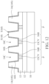
- an isolation structure 14 is formed over the substrate 10 , and the isolation structure 14 has (or is divided into) isolation segments 14 S in a cross-sectional view (e.g. cross-sectional view shown in FIG. 4 ) and is electrically non-conductive. Moreover, as shown in FIG. 4 , in some embodiments, the isolation segments 14 S form concave tanks 14 C that define pixel regions P. In more detail, the isolation structure 14 is formed from the holes 14 H to form the concave tanks 14 C that define pixel regions P. In other words, the bottom electrodes 16 B are formed at bottoms of the concave tanks 14 C, and the circuit layer 12 is disposed between the substrate 10 and the isolation structure 14 .
- the isolation structure 14 may include the same or similar material as the isolation layer 13 . That is, the isolation structure 14 is electrically non-conductive.
- the formation of the isolation structure 14 may include using suitable deposition techniques, examples of which have been described above and will not be repeated here. After the material for the isolation structure 14 is deposited, photolithography and etching processes are performed to form the isolation structure 14 .
- the cross-sectional profile of the isolation structure 14 may be adjusted by the etching conditions to obtain desired shapes.
- the isolation structure 14 in the cross-sectional view i.e., isolation segments 14 S
- each isolation segment 14 S has a trapezoidal shape.
- the maximum width W 14 S of the isolation segment 14 S in the cross-sectional view is greater than or equal to about 100 nm.
- the maximum width W 14 S of the isolation segment 14 S is the bottommost width of the isolation segment 14 S, but the present disclosure is not limited thereto.
- the height H 14 S of the isolation segment 14 S in the cross-sectional view is greater than or equal to about 50 nm.
- the present disclosure is not limited thereto.
- the bottom electrodes 16 B extend into bottoms of the isolation segments 14 S.
- each concave tank 14 C corresponds to one bottom electrode 16 B, and the bottom electrodes 16 B are electrically connected to the circuit layer 12 through the contact vias 13 CV. That is, the concave tank 14 C exposes at least one portion of the corresponding bottom electrode 16 B, but the present disclosure is not limited thereto.
- the maximum width W 14 C of each concave tank 14 C in the cross-sectional view is greater than or equal to about 100 nm.
- the maximum width W 14 C of each concave tank 14 C is the topmost width of the each concave tank 14 C, but the present disclosure is not limited thereto.
- a second conductive layer 16 - 2 is formed on the isolation structure 14 .
- the second conductive layer 16 - 2 is formed on the topmost surface S 14 S of the isolation structure 14 (isolation segment 14 S) and the sidewalls of the isolation segment 14 S (or the sidewalls of the concave tank 14 C).
- the second conductive layer 16 - 2 may include the same or similar material as the first conductive layer 16 - 1 .
- the first conductive layer 16 - 1 and the second conductive layer 16 - 2 may include titanium (Ti), titanium nitride (TiN), aluminum (Al), or silver (Ag), but the present disclosure is not limited thereto.
- the first conductive layer 16 - 1 and the second conductive layer 16 - 2 are different.
- the formation of the second conductive layer 16 - 2 may include using suitable deposition techniques, examples of which have been described above and will not be repeated here.
- reflective layers 16 S are formed on sidewalls of the concave tanks 14 C.
- a portion of the second conductive layer 16 - 2 on the topmost surface S 14 S of the isolation structure 14 is removed to form the reflective layers 16 S on the sidewalls of the concave tanks 14 C.
- the portion of the second conductive layer 16 - 2 on the topmost surface S 14 S of the isolation structure 14 may be removed by a chemical mechanical polishing (CMP) process, but the present disclosure is not limited thereto.
- CMP chemical mechanical polishing
- the reflective layers 16 S include a conductive material, and/or the reflective layers 16 S include the same material as the bottom electrodes 16 B, but the present disclosure is not limited thereto.
- the top surface S 16 S of each reflective layer 16 S is aligned with or lower than the topmost surface S 14 S of the isolation structure 14 (the corresponding isolation segment 14 S). That is, the top surface S 16 S of the reflective layer 16 S and the topmost surface S 14 S of the isolation structure 14 (the isolation segment 14 S) may be coplanar, or the top surface S 16 S of the reflective layer 16 S may be lower than the topmost surface S 14 S of the isolation structure 14 (the isolation segment 14 S). Moreover, in some embodiments, the thickness T 16 S of the reflective layer 16 S is greater than or equal to about 20 nm.
- the reflective layer 16 S may be used to reflect light, so that wide-angle incident light may be blocked in the concave tank 14 C to be transported into the corresponding pixel region P and may be prevented from reaching the neighbor pixel region P, thereby effectively improving optical cross-talk among pixels.
- the included angle ⁇ between the bottom electrode 16 B and the corresponding reflective layer 16 S in the cross-sectional view is between about 90° and about 135°. If the included angle ⁇ is less than 90°, then the subsequently formed photoelectric conversion layer 18 is more difficult to fill in the concave tanks 14 C. If the included angle ⁇ is greater than 135°, then optical cross-talk among pixels may not be effectively improved.
- a photoelectric conversion layer 18 is formed on the isolation structure 14 and in the concave tanks 14 C.
- the photoelectric conversion layer 18 fills the concave tanks 14 C.
- the photoelectric conversion layer 18 may include a material that absorbs light irradiation and generates signal charges corresponding to an amount of the absorbed light, such as an organic material, a perovskite material, a quantum dots material, any other applicable material, or a combination thereof.
- the photoelectric conversion layer 18 may be formed by a deposition process, and the deposition process may include spin coating, thermal evaporation, a combination thereof, or the like, but the present disclosure is not limited thereto.
- the photoelectric conversion layer 18 may be planarized with a planarization process, such as a chemical mechanical polishing (CMP) process, but the present disclosure is not limited thereto.
- CMP chemical mechanical polishing
- the photoelectric conversion layer 18 includes an electron transport layer (ETL) or a hole transport layer (HTL).
- the photoelectric conversion layer 18 may include titanium dioxide (TiO 2 ), but the present disclosure is not limited thereto.
- a top electrode 16 T is formed on the photoelectric conversion layer 18 .
- the top electrode 16 T may include the same or similar material as the bottom electrodes 16 B, but the present disclosure is not limited thereto.
- the formation of the top electrode 16 T may include using suitable deposition techniques, examples of which have been described above and will not be repeated here.
- the top electrode 16 T may be planarized with a planarization process, such as a chemical mechanical polishing (CMP) process, to form a substantially flat top surface, but the present disclosure is not limited thereto.
- CMP chemical mechanical polishing
- an encapsulation layer 20 is formed on the top electrode 16 T to form the image sensor 100 .
- the encapsulation layer 20 may include silicon nitride, silicon oxide, silicon oxynitride, aluminum oxide, any other applicable material, or a combination thereof.
- the formation of the encapsulation layer 20 may include using suitable deposition techniques, examples of which have been described above and will not be repeated here.
- the encapsulation layer 20 may be planarized with a planarization process, such as a chemical mechanical polishing (CMP) process, to form a substantially flat top surface, but the present disclosure is not limited thereto.
- CMP chemical mechanical polishing
- the image sensor 100 includes a substrate 10 and an isolation structure 14 disposed over the substrate 10 .
- the isolation structure 14 has isolation segments 14 S in a cross-sectional view and is electrically non-conductive, and the isolation segments 14 S form concave tanks 14 C that define pixel regions P.
- the image sensor 100 also includes bottom electrodes 16 B disposed at bottoms of the concave tanks 14 C and reflective layers 16 S disposed on sidewalls of the concave tanks 14 C.
- the image sensor 100 further includes a photoelectric conversion layer 18 disposed on the isolation structure 14 and in the concave tanks 14 C and a top electrode 16 T disposed on the photoelectric conversion layer 18 .
- the image sensor 100 includes an encapsulation layer 20 disposed on the top electrode 16 T.
- optical cross-talk among pixels may be effectively improved duo to the reflective layers 16 S on sidewalls of the concave tanks 14 C.
- charge carrier absorption in the photoelectric conversion layer 18 may also be increased duo to the reflective layers 16 S on sidewalls of the concave tanks 14 C, thereby increasing sensitivity of the image sensor 100 .
- FIG. 9 is a cross-sectional view illustrating a portion of the image sensor 100 at additional stages in the manufacturing of the image sensor 100 in accordance with some other embodiments of the present disclosure. Similarly, some components of the image sensor 100 have been omitted in FIG. 9 for the sake of brevity.
- condensing structures 24 are formed above the encapsulation layer 20 , and each condensing structure 24 corresponds to one pixel region P.
- the condensing structure 24 may include glass, epoxy resin, silicone resin, polyurethane, any other applicable material, or a combination thereof, but the present disclosure is not limited thereto.
- the condensing structure 24 may be formed by a photoresist reflow method, a hot embossing method, any other applicable method, or a combination thereof.
- the steps of forming the condensing structure 24 may include a spin coating process, a lithography process, an etching process, any other applicable process, or a combination thereof, but the present disclosure is not limited thereto.
- the condensing structure 24 is a micro-lens for converging the incident light.
- the micro-lens may include a semi-convex lens or a convex lens, but the present disclosure is not limited thereto.
- the condensing structure 24 may also include micro-pyramid structures (e.g., circular cone, quadrangular pyramid, and so on), or micro-trapezoidal structures (e.g., flat top cone, truncated square pyramid, and so on).
- the condensing structure 24 may be a gradient-index structure.
- the image sensor 100 further includes a color filter layer 22 disposed between the encapsulation layer 20 and the condensing structures 24 .
- the color filter layer 20 has (or is divided into) color filter segments 22 S in the cross-sectional view (e.g., cross-sectional view shown in FIG. 9 ), and the color filter segments 22 S correspond to the concave tanks 14 C and the pixel regions P.
- the color filter segments 22 S capture different color information.
- the color filter layer 22 may have a blue color filter segment, a green color filter segment, and/or a red color filter segment, but the present disclosure is not limited thereto.
- the color filter layer 22 may have a yellow color filter segment, a white color filter segment, a cyan color filter segment, a magenta color filter segment, or an IR/NIR color filter, but the present disclosure is not limited thereto.
- FIG. 10 to FIG. 12 are cross-sectional views illustrating a portion of the image sensor 100 at various stages in the manufacturing of the image sensor 100 in accordance with some other embodiments of the present disclosure.
- the stages shown in FIG. 10 to FIG. 12 may replace the stages shown in FIG. 2 to FIG. 6 .
- some components of the image sensor 100 have been omitted in FIG. 10 to FIG. 12 for the sake of brevity.
- an isolation structure 14 is formed over the substrate 10 , and the isolation structure 14 has (or is divided into) isolation segments 14 S in a cross-sectional view (e.g. cross-sectional view shown in FIG. 10 ) and is electrically non-conductive. Moreover, as shown in FIG. 10 , in some embodiments, the isolation segments 14 S form concave tanks 14 C that define pixel regions P. In more detail, the isolation structure 14 is formed directly on the isolation layer 13 , and each contact vias 13 CV is between two adjacent isolation segments 14 S.
- a cover layer 16 is formed on the isolation structure 14 .
- the cover layer 16 is disposed on the bottoms and sidewalls of the concave tanks 14 C and the topmost surfaces (S 14 S) of the isolation structure 14 (the isolation segments 14 S).
- the cover layer 16 may include a conductive material, such as metal, metal silicide, the like, or a combination thereof, but the present disclosure is not limited thereto.
- the metal may include gold (Au), nickel (Ni), platinum (Pt), palladium (Pd), iridium (Ir), titanium (Ti), chromium (Cr), tungsten (W), aluminum (Al), copper (Cu), the like, an alloy thereof, or a combination thereof, but the present disclosure is not limited thereto.
- the cover layer 16 may be formed by physical vapor deposition (PVD), chemical vapor deposition (CVD), atomic layer deposition (ALD), evaporation, sputtering, the like, or a combination thereof, but the present disclosure is not limited thereto.
- a portion of the cover layer 16 on the topmost surface S 14 S of the isolation structure 14 is removed to form bottom electrodes 16 B at the bottoms of the concave tanks 14 C and reflective layers 16 S on the sidewalls of the concave tanks 14 C.
- the portion of the cover layer 16 on the topmost surface S 14 S of the isolation structure 14 may be removed by a chemical mechanical polishing (CMP) process, but the present disclosure is not limited thereto.
- the reflective layers 16 S include the same material as the bottom electrodes 16 B.
- the image sensor according to the embodiments of the present disclosure includes reflective layers on sidewalls of the concave tanks of the isolation structure. Therefore, wide-angle incident light may be blocked in the concave tank to be transported into the corresponding pixel and may be prevented from reaching the neighbor pixel, thereby effectively improving optical cross-talk among pixels. Moreover, charge carrier absorption may be increased duo to the reflective layers on sidewalls of the concave tanks, thereby increasing sensitivity of the image sensor.
Landscapes
- Solid State Image Pick-Up Elements (AREA)
Abstract
Description
- The present invention relates to an image sensor, and, in particular, to an image sensor that includes reflective layers on sidewalls of the concave tanks of the isolation structure and a method for forming the same.
- Image sensors (e.g., charge-coupled device (CCD) image sensors, complementary metal-oxide semiconductor (CMOS) image sensors, and so on) have been widely used in various image-capturing apparatuses such as digital still-image cameras, digital video cameras, and the like. The light-sensing portion in the image sensor may be formed at each of pixels, and signal electric charges may be generated according to the amount of light received in the light-sensing portion. In addition, the signal electric charges generated in the light-sensing portion may be transmitted and amplified, whereby an image signal is obtained.
- Recently, the trend has been for the pixel size of image sensors typified by CMOS image sensors to be reduced for the purpose of increasing the number of pixels per unit area so as to provide high-resolution images. However, while pixel size continues to decrease, there are still various challenges in the design and manufacturing of image sensors. For example, it is difficult for wide-angle incident light to be absorbed by existing image sensors. Moreover, optical cross-talk among pixels will be a serious problem with smaller pixel sizes, and this may have an adverse influence on the performance of the image sensors. New manufacturing techniques are also needed to further decrease the pixel size without leading to serious optical cross-talk among pixels. Therefore, these and related issues need to be addressed by improving the design and manufacture of image sensors.
- According to the present disclosure, an image sensor that includes reflective layers on sidewalls of the concave tanks of the isolation structure is provided. Wide-angle incident light may be blocked in the concave tank to be transported into the corresponding pixel and may be prevented from reaching the neighbor pixel, so that optical cross-talk among pixels may be effectively improved. Moreover, charge carrier absorption may be increased duo to the reflective layers on sidewalls of the concave tanks, thereby increasing sensitivity of the image sensor.
- An embodiment of the present invention provides an image sensor. The image sensor includes a substrate and an isolation structure disposed over the substrate. The isolation structure has isolation segments in a cross-sectional view and is electrically non-conductive, and the isolation segments form concave tanks that define pixel regions. The image sensor also includes bottom electrodes disposed at bottoms of the concave tanks and reflective layers disposed on sidewalls of the concave tanks. The image sensor further includes a photoelectric conversion layer disposed on the isolation structure and in the concave tanks and a top electrode disposed on the photoelectric conversion layer. Moreover, the image sensor includes an encapsulation layer disposed on the top electrode.
- In some embodiments, the reflective layers include a conductive material.
- In some embodiments, the reflective layers include the same material as the bottom electrodes.
- In some embodiments, the included angle between each bottom electrode and the corresponding reflective layer in the cross-sectional view is between 90° and 135°.
- In some embodiments, the thickness of the reflective layers is greater than or equal to 20 nm.
- In some embodiments, the maximum width the concave tank in the cross-sectional view is greater than or equal to 100 nm.
- In some embodiments, the maximum width of the isolation segment in the cross-sectional view is greater than or equal to 100 nm.
- In some embodiments, the height of the isolation segment in the cross-sectional view is greater than or equal to 50 nm.
- In some embodiments, portions of the bottom electrodes extend into bottoms of the isolation segments.
- In some embodiments, the top surface of the reflective layer is aligned with or lower than the topmost surface of the corresponding isolation segment.
- In some embodiments, the image sensor further includes condensing structures disposed above the encapsulation layer. Each condensing structure corresponds to one pixel region.
- In some embodiments, the image sensor further includes a color filter layer disposed between the encapsulation layer and the condensing structures.
- In some embodiments, the color filter layer has color filter segments in the cross-sectional view, and the color filter segments correspond to the concave tanks.
- In some embodiments, the color filter segments capture different color information.
- In some embodiments, the image sensor further includes a circuit layer disposed between the substrate and the isolation structure. The bottom electrodes are electrically connected to the circuit layer.
- An embodiment of the present invention provides a method for forming an image sensor. The method for forming the image sensor includes the following steps. An isolation structure is formed over a substrate. The isolation structure has isolation segments in a cross-sectional view and is electrically non-conductive, and the isolation segments form concave tanks. Bottom electrodes are formed at bottoms of the concave tanks.
- Reflective layers are formed on sidewalls of the concave tanks. A photoelectric conversion layer is formed on the isolation structure and in the concave tanks. A top electrode is formed on the photoelectric conversion layer. An encapsulation layer is formed on the top electrode.
- In some embodiments, forming the bottom electrodes and the reflective layers includes the following steps. A first conductive layer is formed over the substrate. The first conductive layer is patterned to form the bottom electrodes and holes between the bottom electrodes. The isolation structure is formed from the holes to form the concave tanks that define pixel regions.
- In some embodiments, forming the bottom electrodes and the reflective layers further includes the following steps. A second conductive layer is formed on the isolation structure. A portion of the second conductive layer on the topmost surface of the isolation structure is removed to form the reflective layers on sidewalls of the concave tanks.
- In some embodiments, forming the bottom electrodes and the reflective layers includes the following steps. A cover layer is formed on the isolation structure. The cover layer is disposed on the bottoms and sidewalls of the concave tanks and the topmost surface of the isolation structure. A portion of the cover layer on the topmost surface of the isolation structure is removed to form the bottom electrodes at the bottoms of the concave tanks and the reflective layers on the sidewalls of the concave tanks.
- In some embodiments, the method for forming the image sensor further includes the following step. Condensing structures are formed above the encapsulation layer, and each condensing structure corresponds to one pixel region.
- The disclosure can be more fully understood from the following detailed description when read with the accompanying figures. It is worth noting that, in accordance with standard practice in the industry, various features are not drawn to scale. In fact, the dimensions of the various features may be arbitrarily increased or reduced for clarity of discussion.
-
FIG. 1 is a cross-sectional view illustrating a portion of the image sensor at one stage in the manufacturing of the image sensor in accordance with some embodiments of the present disclosure. -
FIG. 2 is a cross-sectional view illustrating a portion of the image sensor at one stage in the manufacturing of the image sensor in accordance with some embodiments of the present disclosure. -
FIG. 3 is a cross-sectional view illustrating a portion of the image sensor at one stage in the manufacturing of the image sensor in accordance with some embodiments of the present disclosure. -
FIG. 4 is a cross-sectional view illustrating a portion of the image sensor at one stage in the manufacturing of the image sensor in accordance with some embodiments of the present disclosure. -
FIG. 5 is a cross-sectional view illustrating a portion of the image sensor at one stage in the manufacturing of the image sensor in accordance with some embodiments of the present disclosure. -
FIG. 6 is a cross-sectional view illustrating a portion of the image sensor at one stage in the manufacturing of the image sensor in accordance with some embodiments of the present disclosure. -
FIG. 7 is a cross-sectional view illustrating a portion of the image sensor at one stage in the manufacturing of the image sensor in accordance with some embodiments of the present disclosure. -
FIG. 8 is a cross-sectional view illustrating a portion of the image sensor at one stage in the manufacturing of the image sensor in accordance with some embodiments of the present disclosure. -
FIG. 9 is a cross-sectional view illustrating a portion of the image sensor at additional stages in the manufacturing of the image sensor in accordance with some other embodiments of the present disclosure. -
FIG. 10 is a cross-sectional view illustrating a portion of the image sensor at one stage in the manufacturing of the image sensor in accordance with some other embodiments of the present disclosure. -
FIG. 11 is a cross-sectional view illustrating a portion of the image sensor at one stage in the manufacturing of the image sensor in accordance with some other embodiments of the present disclosure. -
FIG. 12 is a cross-sectional view illustrating a portion of the image sensor at one stage in the manufacturing of the image sensor in accordance with some other embodiments of the present disclosure. - The following disclosure provides many different embodiments, or examples, for implementing different features of the subject matter provided. Specific examples of components and arrangements are described below to simplify the present disclosure. These are, of course, merely examples and are not intended to be limiting. For example, a first feature is formed on a second feature in the description that follows may include embodiments in which the first feature and second feature are formed in direct contact, and may also include embodiments in which additional features may be formed between the first feature and second feature, so that the first feature and second feature may not be in direct contact.
- It should be understood that additional steps may be implemented before, during, or after the illustrated methods, and some steps might be replaced or omitted in other embodiments of the illustrated methods.
- Furthermore, spatially relative terms, such as “beneath,” “below,” “lower,” “on,” “above,” “upper” and the like, may be used herein for ease of description to describe one element or feature's relationship to other elements or features as illustrated in the figures.
- The spatially relative terms are intended to encompass different orientations of the device in use or operation in addition to the orientation depicted in the figures. The apparatus may be otherwise oriented (rotated 90 degrees or at other orientations) and the spatially relative descriptors used herein may likewise be interpreted accordingly.
- In the present disclosure, the terms “about,” “approximately” and “substantially” typically mean +/−20% of the stated value, more typically +/−10% of the stated value, more typically +/−5% of the stated value, more typically +/−3% of the stated value, more typically +/−2% of the stated value, more typically +/−1% of the stated value and even more typically +/−0.5% of the stated value. The stated value of the present disclosure is an approximate value. That is, when there is no specific description of the terms “about,” “approximately” and “substantially”, the stated value includes the meaning of “about,” “approximately” or “substantially”.
- Unless otherwise defined, all terms (including technical and scientific terms) used herein have the same meaning as commonly understood by one of ordinary skill in the art to which this disclosure belongs. It should be understood that terms such as those defined in commonly used dictionaries should be interpreted as having a meaning that is consistent with their meaning in the context of the relevant art and will not be interpreted in an idealized or overly formal sense unless expressly so defined in the embodiments of the present disclosure.
- The present disclosure may repeat reference numerals and/or letters in following embodiments. This repetition is for the purpose of simplicity and clarity and does not in itself dictate a relationship between the various embodiments and/or configurations discussed.
-
FIG. 1 toFIG. 8 are cross-sectional views illustrating a portion of theimage sensor 100 at various stages in the manufacturing of theimage sensor 100 in accordance with some embodiments of the present disclosure. It should be noted that some components of theimage sensor 100 have been omitted inFIG. 1 toFIG. 8 for the sake of brevity. - Referring to
FIG. 1 , in some embodiments, acircuit layer 12 is formed on asubstrate 10. Thesubstrate 10 may be, for example, a wafer or a chip, but the present disclosure is not limited thereto. Thesubstrate 10 may be a semiconductor substrate, for example, silicon substrate. Furthermore, the semiconductor substrate may also be an elemental semiconductor (e.g., germanium), a compound semiconductor (e.g., gallium nitride (GaN), silicon carbide (SiC), gallium arsenide (GaAs), gallium phosphide (GaP), indium phosphide (InP), indium arsenide (InAs), and/or indium antimonide (InSb)), an alloy semiconductor (e.g., silicon germanium (SiGe) alloy, gallium arsenide phosphide (GaAsP) alloy, aluminum indium arsenide (AlInAs) alloy, aluminum gallium arsenide (AlGaAs) alloy, gallium indium arsenide (GaInAs) alloy, gallium indium phosphide (GaInP) alloy, and/or gallium indium arsenide phosphide (GaInAsP) alloy), the like, or a combination thereof. - The
substrate 10 may include isolation regions (not shown) to separate conductive components formed in thesubstrate 10. The isolation regions may include, for example, shallow trench isolation (STI) regions or deep trench isolation (DTI) regions. The isolation regions may be formed in thesubstrate 10 using an etching process to form trenches and filling the trenches with an insulating or dielectric material, but the present disclosure is not limited thereto. - Moreover, the
circuit layer 12 may be a readout circuit, which may include various conductive features (e.g., conductive lines or vias). For example, the conductive features may be made of aluminum (Al), copper (Cu), tungsten (W), the like, an alloy thereof, any other applicable conductive material, or a combination thereof, but the present disclosure is not limited thereto. - As shown in
FIG. 1 , in some embodiments, anisolation layer 13 is formed on thecircuit layer 12. For example, theisolation layer 13 may include an electrically non-conductive material, such as silicon nitride, silicon oxide, aluminum oxide, photoresist, other suitable materials, or a combination thereof. The formation of theisolation layer 13 may include using suitable deposition techniques, such as physical vapor deposition (PVD), chemical vapor deposition (CVD), atomic layer deposition (ALD), spin coating, the like, or a combination thereof, but the present disclosure is not limited thereto. - As shown in
FIG. 1 , in some embodiments, theisolation layer 13 includes contact vias 13CV that may be used to electrically connect the subsequently formed bottom electrodes (e.g.,bottom electrodes 16B shown inFIG. 3 ) to thecircuit layer 12. Therefore, the positions of the contact vias 13CV may be determined according to the subsequently formed bottom electrodes, but the present disclosure is not limited thereto. - Referring to
FIG. 2 , in some embodiments, a first conductive layer 16-1 is formed over thesubstrate 10. In more detail, the first conductive layer 16-1 is formed on theisolation layer 13. For example, the first conductive layer 16-1 may include a conductive material, such as metal, metal silicide, the like, or a combination thereof, but the present disclosure is not limited thereto. The metal may include gold (Au), nickel (Ni), platinum (Pt), palladium (Pd), iridium (Ir), titanium (Ti), chromium (Cr), tungsten (W), aluminum (Al), copper (Cu), the like, an alloy thereof, or a combination thereof, but the present disclosure is not limited thereto. Moreover, the first conductive layer 16-1 may be formed by physical vapor deposition (PVD), chemical vapor deposition (CVD), atomic layer deposition (ALD), evaporation, sputtering, the like, or a combination thereof, but the present disclosure is not limited thereto. - Referring to
FIG. 3 , in some embodiments, the first conductive layer 16-1 is patterned to formbottom electrodes 16B andholes 14H between thebottom electrodes 16B. For example, a mask layer (not illustrated) may be disposed on the first conductive layer 16-1, and then an etching process may be performed to etch the first conductive layer 16-1 into thebottom electrodes 16B and theholes 14H using the mask layer as an etch mask. The mask layer may include a photoresist, such as a positive photoresist or a negative photoresist. Moreover, the mask layer may be a hard mask and may include silicon oxide (SiO2), silicon nitride (SiN), silicon oxynitride (SiON), silicon carbide (SiC), silicon carbonitride (SiCN), the like, or a combination thereof, but the present disclosure is not limited thereto. - The mask layer may be a single-layer structure or a multi-layer structure, and may be formed by a deposition process, a photolithography process, any other applicable process, or a combination thereof, but the present disclosure is not limited thereto. For example, the deposition process may include spin-on coating, chemical vapor deposition (CVD), atomic layer deposition (ALD), the like, or a combination thereof. For example, the photolithography process may include photoresist coating (e.g., spin coating), soft baking, mask aligning, exposure, post-exposure baking (PEB), developing, rinsing, drying (e.g., hard baking), other suitable processes, or a combination thereof, but the present disclosure is not limited thereto.
- The etching process may include a dry etching process, a wet etching process, or a combination thereof. For example, the dry etching process may include reactive ion etch (RIE), inductively-coupled plasma (ICP) etching, neutral beam etching (NBE), electron cyclotron resonance (ERC) etching, the like, or a combination thereof, but the present disclosure is not limited thereto. For example, the wet etching process may use, for example, hydrofluoric acid (HF), ammonium hydroxide (NH4OH), or any suitable etchant.
- Referring to
FIG. 4 , in some embodiments, anisolation structure 14 is formed over thesubstrate 10, and theisolation structure 14 has (or is divided into)isolation segments 14S in a cross-sectional view (e.g. cross-sectional view shown inFIG. 4 ) and is electrically non-conductive. Moreover, as shown inFIG. 4 , in some embodiments, theisolation segments 14S formconcave tanks 14C that define pixel regions P. In more detail, theisolation structure 14 is formed from theholes 14H to form theconcave tanks 14C that define pixel regions P. In other words, thebottom electrodes 16B are formed at bottoms of theconcave tanks 14C, and thecircuit layer 12 is disposed between thesubstrate 10 and theisolation structure 14. - The
isolation structure 14 may include the same or similar material as theisolation layer 13. That is, theisolation structure 14 is electrically non-conductive. The formation of theisolation structure 14 may include using suitable deposition techniques, examples of which have been described above and will not be repeated here. After the material for theisolation structure 14 is deposited, photolithography and etching processes are performed to form theisolation structure 14. The cross-sectional profile of theisolation structure 14 may be adjusted by the etching conditions to obtain desired shapes. For example, theisolation structure 14 in the cross-sectional view (i.e.,isolation segments 14S) may have a rectangular shape, a trapezoidal shape, an inversely trapezoidal shape, or a triangular shape, but the present disclosure is not limited thereto. - In the embodiment shown in
FIG. 4 , eachisolation segment 14S has a trapezoidal shape. In this embodiment, the maximum width W14S of theisolation segment 14S in the cross-sectional view is greater than or equal to about 100 nm. Here, the maximum width W14S of theisolation segment 14S is the bottommost width of theisolation segment 14S, but the present disclosure is not limited thereto. Moreover, in this embodiment, the height H14S of theisolation segment 14S in the cross-sectional view is greater than or equal to about 50 nm. However, the present disclosure is not limited thereto. - As shown in
FIG. 4 , in some embodiments, thebottom electrodes 16B extend into bottoms of theisolation segments 14S. Moreover, in some embodiments, eachconcave tank 14C corresponds to onebottom electrode 16B, and thebottom electrodes 16B are electrically connected to thecircuit layer 12 through the contact vias 13CV. That is, theconcave tank 14C exposes at least one portion of the correspondingbottom electrode 16B, but the present disclosure is not limited thereto. In the embodiment shown inFIG. 4 , the maximum width W14C of eachconcave tank 14C in the cross-sectional view is greater than or equal to about 100 nm. Here, the maximum width W14C of eachconcave tank 14C is the topmost width of the eachconcave tank 14C, but the present disclosure is not limited thereto. - Referring to
FIG. 5 , in some embodiments, a second conductive layer 16-2 is formed on theisolation structure 14. In more detail, the second conductive layer 16-2 is formed on the topmost surface S14S of the isolation structure 14 (isolation segment 14S) and the sidewalls of theisolation segment 14S (or the sidewalls of theconcave tank 14C). For example, the second conductive layer 16-2 may include the same or similar material as the first conductive layer 16-1. In some embodiment, the first conductive layer 16-1 and the second conductive layer 16-2 may include titanium (Ti), titanium nitride (TiN), aluminum (Al), or silver (Ag), but the present disclosure is not limited thereto. In some other embodiments, the first conductive layer 16-1 and the second conductive layer 16-2 are different. Moreover, the formation of the second conductive layer 16-2 may include using suitable deposition techniques, examples of which have been described above and will not be repeated here. - Referring to
FIG. 6 , in some embodiments,reflective layers 16S are formed on sidewalls of theconcave tanks 14C. In this embodiment, a portion of the second conductive layer 16-2 on the topmost surface S14S of theisolation structure 14 is removed to form thereflective layers 16S on the sidewalls of theconcave tanks 14C. For example, the portion of the second conductive layer 16-2 on the topmost surface S14S of theisolation structure 14 may be removed by a chemical mechanical polishing (CMP) process, but the present disclosure is not limited thereto. In this embodiment, thereflective layers 16S include a conductive material, and/or thereflective layers 16S include the same material as thebottom electrodes 16B, but the present disclosure is not limited thereto. - As shown in
FIG. 6 , in some embodiments, the top surface S16S of eachreflective layer 16S is aligned with or lower than the topmost surface S14S of the isolation structure 14 (thecorresponding isolation segment 14S). That is, the top surface S16S of thereflective layer 16S and the topmost surface S14S of the isolation structure 14 (theisolation segment 14S) may be coplanar, or the top surface S16S of thereflective layer 16S may be lower than the topmost surface S14S of the isolation structure 14 (theisolation segment 14S). Moreover, in some embodiments, the thickness T16S of thereflective layer 16S is greater than or equal to about 20 nm. - In the embodiments of the present disclosure, the
reflective layer 16S may be used to reflect light, so that wide-angle incident light may be blocked in theconcave tank 14C to be transported into the corresponding pixel region P and may be prevented from reaching the neighbor pixel region P, thereby effectively improving optical cross-talk among pixels. As shown inFIG. 6 , in some embodiments, the included angle θ between thebottom electrode 16B and the correspondingreflective layer 16S in the cross-sectional view is between about 90° and about 135°. If the included angle θ is less than 90°, then the subsequently formedphotoelectric conversion layer 18 is more difficult to fill in theconcave tanks 14C. If the included angle θ is greater than 135°, then optical cross-talk among pixels may not be effectively improved. - Referring to
FIG. 7 , in some embodiments, aphotoelectric conversion layer 18 is formed on theisolation structure 14 and in theconcave tanks 14C. In more detail, thephotoelectric conversion layer 18 fills theconcave tanks 14C. For example, thephotoelectric conversion layer 18 may include a material that absorbs light irradiation and generates signal charges corresponding to an amount of the absorbed light, such as an organic material, a perovskite material, a quantum dots material, any other applicable material, or a combination thereof. Thephotoelectric conversion layer 18 may be formed by a deposition process, and the deposition process may include spin coating, thermal evaporation, a combination thereof, or the like, but the present disclosure is not limited thereto. Moreover, thephotoelectric conversion layer 18 may be planarized with a planarization process, such as a chemical mechanical polishing (CMP) process, but the present disclosure is not limited thereto. - In some embodiments, the
photoelectric conversion layer 18 includes an electron transport layer (ETL) or a hole transport layer (HTL). For example, thephotoelectric conversion layer 18 may include titanium dioxide (TiO2), but the present disclosure is not limited thereto. - Referring to
FIG. 8 , in some embodiments, atop electrode 16T is formed on thephotoelectric conversion layer 18. For example, thetop electrode 16T may include the same or similar material as thebottom electrodes 16B, but the present disclosure is not limited thereto. The formation of thetop electrode 16T may include using suitable deposition techniques, examples of which have been described above and will not be repeated here. Moreover, thetop electrode 16T may be planarized with a planarization process, such as a chemical mechanical polishing (CMP) process, to form a substantially flat top surface, but the present disclosure is not limited thereto. - Then, as shown in
FIG. 8 , in some embodiments, anencapsulation layer 20 is formed on thetop electrode 16T to form theimage sensor 100. For example, theencapsulation layer 20 may include silicon nitride, silicon oxide, silicon oxynitride, aluminum oxide, any other applicable material, or a combination thereof. The formation of theencapsulation layer 20 may include using suitable deposition techniques, examples of which have been described above and will not be repeated here. Moreover, theencapsulation layer 20 may be planarized with a planarization process, such as a chemical mechanical polishing (CMP) process, to form a substantially flat top surface, but the present disclosure is not limited thereto. - As shown in
FIG. 8 , in some embodiments, theimage sensor 100 includes asubstrate 10 and anisolation structure 14 disposed over thesubstrate 10. Theisolation structure 14 hasisolation segments 14S in a cross-sectional view and is electrically non-conductive, and theisolation segments 14S formconcave tanks 14C that define pixel regions P. Theimage sensor 100 also includesbottom electrodes 16B disposed at bottoms of theconcave tanks 14C andreflective layers 16S disposed on sidewalls of theconcave tanks 14C. Theimage sensor 100 further includes aphotoelectric conversion layer 18 disposed on theisolation structure 14 and in theconcave tanks 14C and atop electrode 16T disposed on thephotoelectric conversion layer 18. Moreover, theimage sensor 100 includes anencapsulation layer 20 disposed on thetop electrode 16T. - In the embodiments of the present disclosure, optical cross-talk among pixels may be effectively improved duo to the
reflective layers 16S on sidewalls of theconcave tanks 14C. Moreover, charge carrier absorption in thephotoelectric conversion layer 18 may also be increased duo to thereflective layers 16S on sidewalls of theconcave tanks 14C, thereby increasing sensitivity of theimage sensor 100. -
FIG. 9 is a cross-sectional view illustrating a portion of theimage sensor 100 at additional stages in the manufacturing of theimage sensor 100 in accordance with some other embodiments of the present disclosure. Similarly, some components of theimage sensor 100 have been omitted inFIG. 9 for the sake of brevity. - Referring to
FIG. 9 , in some embodiments, condensingstructures 24 are formed above theencapsulation layer 20, and each condensingstructure 24 corresponds to one pixel region P. For example, the condensingstructure 24 may include glass, epoxy resin, silicone resin, polyurethane, any other applicable material, or a combination thereof, but the present disclosure is not limited thereto. Moreover, the condensingstructure 24 may be formed by a photoresist reflow method, a hot embossing method, any other applicable method, or a combination thereof. The steps of forming the condensingstructure 24 may include a spin coating process, a lithography process, an etching process, any other applicable process, or a combination thereof, but the present disclosure is not limited thereto. - In some embodiments, the condensing
structure 24 is a micro-lens for converging the incident light. For example, the micro-lens may include a semi-convex lens or a convex lens, but the present disclosure is not limited thereto. The condensingstructure 24 may also include micro-pyramid structures (e.g., circular cone, quadrangular pyramid, and so on), or micro-trapezoidal structures (e.g., flat top cone, truncated square pyramid, and so on). Alternatively, the condensingstructure 24 may be a gradient-index structure. - As shown in
FIG. 9 , in some embodiments, theimage sensor 100 further includes acolor filter layer 22 disposed between theencapsulation layer 20 and the condensingstructures 24. In some embodiments, thecolor filter layer 20 has (or is divided into)color filter segments 22S in the cross-sectional view (e.g., cross-sectional view shown inFIG. 9 ), and thecolor filter segments 22S correspond to theconcave tanks 14C and the pixel regions P. - In some embodiments, the
color filter segments 22S capture different color information. For example, thecolor filter layer 22 may have a blue color filter segment, a green color filter segment, and/or a red color filter segment, but the present disclosure is not limited thereto. In some other examples, thecolor filter layer 22 may have a yellow color filter segment, a white color filter segment, a cyan color filter segment, a magenta color filter segment, or an IR/NIR color filter, but the present disclosure is not limited thereto. -
FIG. 10 toFIG. 12 are cross-sectional views illustrating a portion of theimage sensor 100 at various stages in the manufacturing of theimage sensor 100 in accordance with some other embodiments of the present disclosure. For example, the stages shown inFIG. 10 toFIG. 12 may replace the stages shown inFIG. 2 toFIG. 6 . Similarly, some components of theimage sensor 100 have been omitted inFIG. 10 toFIG. 12 for the sake of brevity. - Referring to
FIG. 10 , continuing fromFIG. 1 , in some embodiments, anisolation structure 14 is formed over thesubstrate 10, and theisolation structure 14 has (or is divided into)isolation segments 14S in a cross-sectional view (e.g. cross-sectional view shown inFIG. 10 ) and is electrically non-conductive. Moreover, as shown inFIG. 10 , in some embodiments, theisolation segments 14S formconcave tanks 14C that define pixel regions P. In more detail, theisolation structure 14 is formed directly on theisolation layer 13, and each contact vias 13CV is between twoadjacent isolation segments 14S. - Referring to
FIG. 11 , in some embodiments, acover layer 16 is formed on theisolation structure 14. As shown inFIG. 11 , thecover layer 16 is disposed on the bottoms and sidewalls of theconcave tanks 14C and the topmost surfaces (S14S) of the isolation structure 14 (theisolation segments 14S). For example, thecover layer 16 may include a conductive material, such as metal, metal silicide, the like, or a combination thereof, but the present disclosure is not limited thereto. The metal may include gold (Au), nickel (Ni), platinum (Pt), palladium (Pd), iridium (Ir), titanium (Ti), chromium (Cr), tungsten (W), aluminum (Al), copper (Cu), the like, an alloy thereof, or a combination thereof, but the present disclosure is not limited thereto. Moreover, thecover layer 16 may be formed by physical vapor deposition (PVD), chemical vapor deposition (CVD), atomic layer deposition (ALD), evaporation, sputtering, the like, or a combination thereof, but the present disclosure is not limited thereto. - Referring to
FIG. 12 , in some embodiments, a portion of thecover layer 16 on the topmost surface S14S of theisolation structure 14 is removed to formbottom electrodes 16B at the bottoms of theconcave tanks 14C andreflective layers 16S on the sidewalls of theconcave tanks 14C. For example, the portion of thecover layer 16 on the topmost surface S14S of theisolation structure 14 may be removed by a chemical mechanical polishing (CMP) process, but the present disclosure is not limited thereto. In this embodiment, thereflective layers 16S include the same material as thebottom electrodes 16B. - As noted above, the image sensor according to the embodiments of the present disclosure includes reflective layers on sidewalls of the concave tanks of the isolation structure. Therefore, wide-angle incident light may be blocked in the concave tank to be transported into the corresponding pixel and may be prevented from reaching the neighbor pixel, thereby effectively improving optical cross-talk among pixels. Moreover, charge carrier absorption may be increased duo to the reflective layers on sidewalls of the concave tanks, thereby increasing sensitivity of the image sensor.
- The foregoing outlines features of several embodiments so that those skilled in the art may better understand the aspects of the present disclosure. Those skilled in the art should appreciate that they may readily use the present disclosure as a basis for designing or modifying other processes and structures for carrying out the same purposes and/or achieving the same advantages of the embodiments introduced herein. Those skilled in the art should also realize that such equivalent constructions do not depart from the spirit and scope of the present disclosure, and that they may make various changes, substitutions, and alterations herein without departing from the spirit and scope of the present disclosure. Therefore, the scope of protection should be determined through the claims. In addition, although some embodiments of the present disclosure are disclosed above, they are not intended to limit the scope of the present disclosure.
- Reference throughout this specification to features, advantages, or similar language does not imply that all of the features and advantages that may be realized with the present disclosure should be or are in any single embodiment of the disclosure. Rather, language referring to the features and advantages is understood to mean that a specific feature, advantage, or characteristic described in connection with an embodiment is included in at least one embodiment of the present disclosure. Thus, discussions of the features and advantages, and similar language, throughout this specification may, but do not necessarily, refer to the same embodiment.
- Furthermore, the described features, advantages, and characteristics of the disclosure may be combined in any suitable manner in one or more embodiments. One skilled in the relevant art will recognize, in light of the description herein, that the disclosure can be practiced without one or more of the specific features or advantages of a particular embodiment. In other instances, additional features and advantages may be recognized in certain embodiments that may not be present in all embodiments of the disclosure.
Claims (20)
Priority Applications (3)
| Application Number | Priority Date | Filing Date | Title |
|---|---|---|---|
| US18/176,854 US20240297193A1 (en) | 2023-03-01 | 2023-03-01 | Image sensor and method for forming the same |
| TW112115500A TWI841360B (en) | 2023-03-01 | 2023-04-26 | Image sensor and method for forming the same |
| CN202310609790.2A CN118588717A (en) | 2023-03-01 | 2023-05-26 | Image sensor and method of forming the same |
Applications Claiming Priority (1)
| Application Number | Priority Date | Filing Date | Title |
|---|---|---|---|
| US18/176,854 US20240297193A1 (en) | 2023-03-01 | 2023-03-01 | Image sensor and method for forming the same |
Publications (1)
| Publication Number | Publication Date |
|---|---|
| US20240297193A1 true US20240297193A1 (en) | 2024-09-05 |
Family
ID=92076982
Family Applications (1)
| Application Number | Title | Priority Date | Filing Date |
|---|---|---|---|
| US18/176,854 Pending US20240297193A1 (en) | 2023-03-01 | 2023-03-01 | Image sensor and method for forming the same |
Country Status (3)
| Country | Link |
|---|---|
| US (1) | US20240297193A1 (en) |
| CN (1) | CN118588717A (en) |
| TW (1) | TWI841360B (en) |
Family Cites Families (6)
| Publication number | Priority date | Publication date | Assignee | Title |
|---|---|---|---|---|
| JP5428394B2 (en) * | 2009-03-04 | 2014-02-26 | ソニー株式会社 | Solid-state imaging device, manufacturing method thereof, and imaging device |
| WO2012161044A1 (en) * | 2011-05-24 | 2012-11-29 | ソニー株式会社 | Semiconductor device |
| TWI495041B (en) * | 2011-07-05 | 2015-08-01 | 新力股份有限公司 | Semiconductor device, manufacturing method for semiconductor device, and electronic device |
| KR102582669B1 (en) * | 2018-10-02 | 2023-09-25 | 삼성전자주식회사 | Image sensor |
| TWI883084B (en) * | 2019-12-17 | 2025-05-11 | 日商索尼半導體解決方案公司 | Light detection device |
| US12148780B2 (en) * | 2021-08-05 | 2024-11-19 | Samsung Electronics Co., Ltd. | Image sensor |
-
2023
- 2023-03-01 US US18/176,854 patent/US20240297193A1/en active Pending
- 2023-04-26 TW TW112115500A patent/TWI841360B/en active
- 2023-05-26 CN CN202310609790.2A patent/CN118588717A/en active Pending
Also Published As
| Publication number | Publication date |
|---|---|
| TWI841360B (en) | 2024-05-01 |
| TW202437526A (en) | 2024-09-16 |
| CN118588717A (en) | 2024-09-03 |
Similar Documents
| Publication | Publication Date | Title |
|---|---|---|
| KR102321856B1 (en) | Deep trench isolation structures resistant to cracking | |
| CN109786407B (en) | Semiconductor image sensor and method of forming the same | |
| KR102456271B1 (en) | Bsi chip with backside alignment mark | |
| CN106057835B (en) | Dielectric grid bottom profile for light focusing | |
| US11843013B2 (en) | Polarizers for image sensor devices | |
| US20250351605A1 (en) | Image sensor | |
| US20080042177A1 (en) | Image sensor and method of fabricating the same | |
| US20220262845A1 (en) | Lens structure configured to increase quantum efficiency of image sensor | |
| US20150264233A1 (en) | Image sensor device with light guiding structure | |
| US20210265514A1 (en) | Image sensor with absorption enhancement structure | |
| US11652133B2 (en) | Image sensor grid and method of manufacturing same | |
| US20240297193A1 (en) | Image sensor and method for forming the same | |
| CN112310128B (en) | Image sensor, semiconductor structure for image sensor and manufacturing method thereof | |
| US20220367559A1 (en) | Method for forming image sensor devices | |
| JP5383124B2 (en) | Solid-state imaging device and manufacturing method thereof | |
| US12279461B2 (en) | Image sensor | |
| US12408460B2 (en) | Image sensor and method of forming the same | |
| US20240421174A1 (en) | Image sensor device and methods of forming the same | |
| TWI905067B (en) | Optical imaging device and method for forming the same | |
| JP2023093317A (en) | Manufacturing method of multi-pixel detector |
Legal Events
| Date | Code | Title | Description |
|---|---|---|---|
| AS | Assignment |
Owner name: VISERA TECHNOLOGIES COMPANY LIMITED, TAIWAN Free format text: ASSIGNMENT OF ASSIGNORS INTEREST;ASSIGNORS:TSAI, WEI-LUNG;WU, CHING-CHIANG;SIGNING DATES FROM 20230220 TO 20230222;REEL/FRAME:062999/0057 |
|
| STPP | Information on status: patent application and granting procedure in general |
Free format text: DOCKETED NEW CASE - READY FOR EXAMINATION |
|
| STPP | Information on status: patent application and granting procedure in general |
Free format text: NON FINAL ACTION COUNTED, NOT YET MAILED |
|
| STPP | Information on status: patent application and granting procedure in general |
Free format text: NON FINAL ACTION MAILED |
|
| STPP | Information on status: patent application and granting procedure in general |
Free format text: RESPONSE TO NON-FINAL OFFICE ACTION ENTERED AND FORWARDED TO EXAMINER |
|
| STPP | Information on status: patent application and granting procedure in general |
Free format text: NON FINAL ACTION COUNTED, NOT YET MAILED |
|
| STPP | Information on status: patent application and granting procedure in general |
Free format text: NON FINAL ACTION MAILED |
|
| STPP | Information on status: patent application and granting procedure in general |
Free format text: RESPONSE TO NON-FINAL OFFICE ACTION ENTERED AND FORWARDED TO EXAMINER |