US20240297170A1 - Semiconductor structure and method for forming the same - Google Patents
Semiconductor structure and method for forming the same Download PDFInfo
- Publication number
- US20240297170A1 US20240297170A1 US18/178,406 US202318178406A US2024297170A1 US 20240297170 A1 US20240297170 A1 US 20240297170A1 US 202318178406 A US202318178406 A US 202318178406A US 2024297170 A1 US2024297170 A1 US 2024297170A1
- Authority
- US
- United States
- Prior art keywords
- gate
- semiconductor
- gate structure
- layer
- nanostructures
- Prior art date
- Legal status (The legal status is an assumption and is not a legal conclusion. Google has not performed a legal analysis and makes no representation as to the accuracy of the status listed.)
- Pending
Links
Images


Classifications
-
- H01L27/088—
-
- H—ELECTRICITY
- H10—SEMICONDUCTOR DEVICES; ELECTRIC SOLID-STATE DEVICES NOT OTHERWISE PROVIDED FOR
- H10D—INORGANIC ELECTRIC SEMICONDUCTOR DEVICES
- H10D84/00—Integrated devices formed in or on semiconductor substrates that comprise only semiconducting layers, e.g. on Si wafers or on GaAs-on-Si wafers
- H10D84/80—Integrated devices formed in or on semiconductor substrates that comprise only semiconducting layers, e.g. on Si wafers or on GaAs-on-Si wafers characterised by the integration of at least one component covered by groups H10D12/00 or H10D30/00, e.g. integration of IGFETs
- H10D84/82—Integrated devices formed in or on semiconductor substrates that comprise only semiconducting layers, e.g. on Si wafers or on GaAs-on-Si wafers characterised by the integration of at least one component covered by groups H10D12/00 or H10D30/00, e.g. integration of IGFETs of only field-effect components
- H10D84/83—Integrated devices formed in or on semiconductor substrates that comprise only semiconducting layers, e.g. on Si wafers or on GaAs-on-Si wafers characterised by the integration of at least one component covered by groups H10D12/00 or H10D30/00, e.g. integration of IGFETs of only field-effect components of only insulated-gate FETs [IGFET]
-
- H01L21/823412—
-
- H01L21/823456—
-
- H—ELECTRICITY
- H10—SEMICONDUCTOR DEVICES; ELECTRIC SOLID-STATE DEVICES NOT OTHERWISE PROVIDED FOR
- H10D—INORGANIC ELECTRIC SEMICONDUCTOR DEVICES
- H10D84/00—Integrated devices formed in or on semiconductor substrates that comprise only semiconducting layers, e.g. on Si wafers or on GaAs-on-Si wafers
- H10D84/01—Manufacture or treatment
- H10D84/0123—Integrating together multiple components covered by H10D12/00 or H10D30/00, e.g. integrating multiple IGBTs
- H10D84/0126—Integrating together multiple components covered by H10D12/00 or H10D30/00, e.g. integrating multiple IGBTs the components including insulated gates, e.g. IGFETs
- H10D84/0128—Manufacturing their channels
-
- H—ELECTRICITY
- H10—SEMICONDUCTOR DEVICES; ELECTRIC SOLID-STATE DEVICES NOT OTHERWISE PROVIDED FOR
- H10D—INORGANIC ELECTRIC SEMICONDUCTOR DEVICES
- H10D84/00—Integrated devices formed in or on semiconductor substrates that comprise only semiconducting layers, e.g. on Si wafers or on GaAs-on-Si wafers
- H10D84/01—Manufacture or treatment
- H10D84/0123—Integrating together multiple components covered by H10D12/00 or H10D30/00, e.g. integrating multiple IGBTs
- H10D84/0126—Integrating together multiple components covered by H10D12/00 or H10D30/00, e.g. integrating multiple IGBTs the components including insulated gates, e.g. IGFETs
- H10D84/0135—Manufacturing their gate conductors
- H10D84/0142—Manufacturing their gate conductors the gate conductors having different shapes or dimensions
-
- H—ELECTRICITY
- H10—SEMICONDUCTOR DEVICES; ELECTRIC SOLID-STATE DEVICES NOT OTHERWISE PROVIDED FOR
- H10D—INORGANIC ELECTRIC SEMICONDUCTOR DEVICES
- H10D84/00—Integrated devices formed in or on semiconductor substrates that comprise only semiconducting layers, e.g. on Si wafers or on GaAs-on-Si wafers
- H10D84/01—Manufacture or treatment
- H10D84/02—Manufacture or treatment characterised by using material-based technologies
- H10D84/03—Manufacture or treatment characterised by using material-based technologies using Group IV technology, e.g. silicon technology or silicon-carbide [SiC] technology
- H10D84/038—Manufacture or treatment characterised by using material-based technologies using Group IV technology, e.g. silicon technology or silicon-carbide [SiC] technology using silicon technology, e.g. SiGe
-
- H—ELECTRICITY
- H10—SEMICONDUCTOR DEVICES; ELECTRIC SOLID-STATE DEVICES NOT OTHERWISE PROVIDED FOR
- H10D—INORGANIC ELECTRIC SEMICONDUCTOR DEVICES
- H10D84/00—Integrated devices formed in or on semiconductor substrates that comprise only semiconducting layers, e.g. on Si wafers or on GaAs-on-Si wafers
- H10D84/80—Integrated devices formed in or on semiconductor substrates that comprise only semiconducting layers, e.g. on Si wafers or on GaAs-on-Si wafers characterised by the integration of at least one component covered by groups H10D12/00 or H10D30/00, e.g. integration of IGFETs
- H10D84/82—Integrated devices formed in or on semiconductor substrates that comprise only semiconducting layers, e.g. on Si wafers or on GaAs-on-Si wafers characterised by the integration of at least one component covered by groups H10D12/00 or H10D30/00, e.g. integration of IGFETs of only field-effect components
- H10D84/83—Integrated devices formed in or on semiconductor substrates that comprise only semiconducting layers, e.g. on Si wafers or on GaAs-on-Si wafers characterised by the integration of at least one component covered by groups H10D12/00 or H10D30/00, e.g. integration of IGFETs of only field-effect components of only insulated-gate FETs [IGFET]
- H10D84/8311—Integrated devices formed in or on semiconductor substrates that comprise only semiconducting layers, e.g. on Si wafers or on GaAs-on-Si wafers characterised by the integration of at least one component covered by groups H10D12/00 or H10D30/00, e.g. integration of IGFETs of only field-effect components of only insulated-gate FETs [IGFET] the IGFETs characterised by having different channel structures
-
- H—ELECTRICITY
- H10—SEMICONDUCTOR DEVICES; ELECTRIC SOLID-STATE DEVICES NOT OTHERWISE PROVIDED FOR
- H10D—INORGANIC ELECTRIC SEMICONDUCTOR DEVICES
- H10D84/00—Integrated devices formed in or on semiconductor substrates that comprise only semiconducting layers, e.g. on Si wafers or on GaAs-on-Si wafers
- H10D84/80—Integrated devices formed in or on semiconductor substrates that comprise only semiconducting layers, e.g. on Si wafers or on GaAs-on-Si wafers characterised by the integration of at least one component covered by groups H10D12/00 or H10D30/00, e.g. integration of IGFETs
- H10D84/82—Integrated devices formed in or on semiconductor substrates that comprise only semiconducting layers, e.g. on Si wafers or on GaAs-on-Si wafers characterised by the integration of at least one component covered by groups H10D12/00 or H10D30/00, e.g. integration of IGFETs of only field-effect components
- H10D84/83—Integrated devices formed in or on semiconductor substrates that comprise only semiconducting layers, e.g. on Si wafers or on GaAs-on-Si wafers characterised by the integration of at least one component covered by groups H10D12/00 or H10D30/00, e.g. integration of IGFETs of only field-effect components of only insulated-gate FETs [IGFET]
- H10D84/832—Integrated devices formed in or on semiconductor substrates that comprise only semiconducting layers, e.g. on Si wafers or on GaAs-on-Si wafers characterised by the integration of at least one component covered by groups H10D12/00 or H10D30/00, e.g. integration of IGFETs of only field-effect components of only insulated-gate FETs [IGFET] comprising IGFETs having stacked nanowire, nanosheet or nanoribbon channels
Definitions
- multi-gate devices have been introduced in an effort to improve gate control by increasing gate-channel coupling, reduce OFF-state current, and reduce short-channel effects (SCEs).
- SCEs short-channel effects
- FIGS. 1 A to 1 E illustrate perspective views of intermediate stages of manufacturing a semiconductor structure in accordance with some embodiments.
- FIG. 2 shows a top-view representation of the semiconductor structure, in accordance with some embodiments.
- FIGS. 3 A- 1 to 3 M- 1 illustrate cross-sectional representations of various stages of manufacturing the semiconductor structure shown along line A-A′ in FIG. 1 E and in FIG. 2 , in accordance with some embodiments.
- FIGS. 3 A- 2 to 3 M- 2 illustrate cross-sectional representations of various stages of manufacturing the semiconductor structure shown along line B-B′ in FIG. 1 E and in FIG. 2 , in accordance with some embodiments.
- FIGS. 3 A- 3 to 3 M- 3 illustrate cross-sectional representations of various stages of manufacturing the semiconductor structure shown along line C 1 -C 1 ′ and C 2 -C 2 ′ in FIG. 1 E and in FIG. 2 , in accordance with some embodiments.
- FIGS. 4 A to 4 C illustrate cross-sectional representations of various stages of manufacturing the semiconductor structure after the first semiconductor material layers are removed, in accordance with some embodiments.
- FIG. 5 illustrates a cross-sectional view of a semiconductor structure, in accordance with some embodiments.
- FIG. 6 shows a top-view representation of a semiconductor structure, in accordance with some embodiments.
- FIGS. 7 A to 7 C illustrate cross-sectional representations of various stages of manufacturing the semiconductor structure shown along line B 1 -B 1 ′, B 2 -B 2 ′ and B 3 -B 3 ′ in FIG. 6 , in accordance with some embodiments.
- FIG. 8 illustrates a perspective view of a semiconductor structure, in accordance with some embodiments
- FIG. 9 shows a top-view representation of the semiconductor structure, in accordance with some embodiments.
- FIGS. 10 A- 1 to 10 F- 1 illustrate cross-sectional representations of various stages of manufacturing the semiconductor structure 100 d shown along line A-A′ in FIG. 8 and in FIG. 9 , in accordance with some embodiments.
- FIGS. 10 A- 2 to 10 D- 2 illustrate cross-sectional representations of various stages of manufacturing the semiconductor structure 100 d shown along line B-B′ in FIG. 8 and in FIG. 9 , in accordance with some embodiments.
- FIGS. 10 E- 2 to 10 F- 2 illustrate cross-sectional representations of various stages of manufacturing the semiconductor structure 100 d shown along line B-B′ and F-F′ in FIG. 8 and in FIG. 9 , in accordance with some embodiments.
- FIGS. 10 A- 3 to 10 B- 3 illustrate cross-sectional representations of various stages of manufacturing the semiconductor structure shown along line D 1 -D 1 ′ in FIG. 8 and in FIG. 9 , in accordance with some embodiments.
- FIGS. 10 C- 3 to 10 D- 3 illustrate cross-sectional representations of various stages of manufacturing the semiconductor structure shown along line D 2 -D 2 ′ in FIG. 8 and in FIG. 9 , in accordance with some embodiments.
- FIGS. 10 E- 3 to 10 F- 3 illustrate cross-sectional representations of various stages of manufacturing the semiconductor structure shown along line C-C′, D 1 -D 1 ′ and E-E′ in FIG. 8 and in FIG. 9 , in accordance with some embodiments.
- FIG. 11 illustrates a cross-sectional view of a semiconductor structure, in accordance with some embodiments.
- FIGS. 12 A- 1 to 12 B- 1 illustrate cross-sectional representations of various stages of manufacturing a semiconductor structure shown along line A-A′ in FIG. 8 and in FIG. 9 , in accordance with some embodiments.
- FIGS. 12 A- 2 to 12 B- 2 illustrate cross-sectional representations of various stages of manufacturing the semiconductor structure shown along line B-B′ in FIG. 8 and in FIG. 9 , in accordance with some embodiments.
- FIGS. 12 A- 3 to 12 B- 3 illustrate cross-sectional representations of various stages of manufacturing the semiconductor structure shown along line C-C′ and E-E′ in FIG. 8 and in FIG. 9 , in accordance with some embodiments.
- FIG. 13 illustrates a cross-sectional view of a semiconductor structure, in accordance with some embodiments.
- first and second features are formed in direct contact
- additional features may be formed between the first and second features, such that the first and second features may not be in direct contact
- present disclosure may repeat reference numerals and/or letters in the various examples. This repetition is for the purpose of simplicity and clarity and does not in itself dictate a relationship between the various embodiments and/or configurations discussed.
- the gate all around (GAA) transistor structures described below may be patterned by any suitable method.
- the structures may be patterned using one or more photolithography processes, including double-patterning or multi-patterning processes.
- double-patterning or multi-patterning processes combine photolithography and self-aligned processes, allowing patterns to be created that have, for example, smaller pitches than what is otherwise obtainable using a single, direct photolithography process.
- a sacrificial layer is formed over a substrate and patterned using a photolithography process. Spacers are formed alongside the patterned sacrificial layer using a self-aligned process. The sacrificial layer is then removed, and the remaining spacers may then be used to pattern the GAA structure.
- the fins described below may be patterned by any suitable method.
- the fins may be patterned using one or more photolithography processes, including double-patterning or multi-patterning processes.
- double-patterning or multi-patterning processes combine photolithography and self-aligned processes, allowing patterns to be created that have, for example, pitches smaller than what is otherwise obtainable using a single, direct photolithography process.
- a sacrificial layer is formed over a substrate and patterned using a photolithography process. Spacers are formed alongside the patterned sacrificial layer using a self-aligned process. The sacrificial layer is then removed, and the remaining spacers may then be used to pattern the fins.
- the semiconductor structures may include a first fin structure and a second fin structure formed over a substrate.
- the first fin structure includes first nanostructures
- the second fin structure includes second nanostructures along a first direction (e.g. x-axis).
- a first gate structure formed over the first nanostructures and a first S/D structure adjacent to the first gate structure.
- a second gate structure formed over the second nanostructures along the second direction (e.g. y-axis).
- a gate spacer layer is adjacent to the gate structure. A portion of the topmost nanostructures is removed, and therefore the number of nanostructures directly below the gate structure is reduced.
- the first width of the first nanostructures along the second direction is smaller than the second width of the second nanostructures along the second direction.
- the first gate structure is formed for power efficiency
- the second gate structure is formed for high speed performance.
- the first gate structure and second gate structure co-exist to achieve multi-nanostructures for speed performance and power efficiency. Therefore, the performance of the semiconductor structure is improved.
- the source/drain (S/D) structure or region(s) may refer to a source or a drain, individually or collectively dependent upon the context.
- FIGS. 1 A to 1 E illustrate perspective views of intermediate stages of manufacturing a semiconductor structure 100 a , in accordance with some embodiments. As shown in FIG. 1 A , first semiconductor material layers 106 and second semiconductor material layers 108 are formed over a substrate 102 .
- the substrate 102 may be a semiconductor wafer such as a silicon wafer.
- the substrate 102 may include elementary semiconductor materials, compound semiconductor materials, and/or alloy semiconductor materials.
- Elementary semiconductor materials may include, but are not limited to, crystal silicon, polycrystalline silicon, amorphous silicon, germanium, and/or diamond.
- Compound semiconductor materials may include, but are not limited to, silicon carbide, gallium arsenic, gallium phosphide, indium phosphide, indium arsenide, and/or indium antimonide.
- Alloy semiconductor materials may include, but are not limited to, SiGe, GaAsP, AlInAs, AlGaAs, GaInAs, GaInP, and/or GaInAsP.
- the first semiconductor material layers 106 and the second semiconductor material layers 108 are alternately stacked over the substrate 102 .
- the first semiconductor material layers 106 and the second semiconductor material layers 108 are made of different semiconductor materials.
- the first semiconductor material layers 106 are made of SiGe
- the second semiconductor material layers 108 are made of silicon. It should be noted that although three first semiconductor material layers 106 and three second semiconductor material layers 108 are formed, the semiconductor structure may include more or fewer first semiconductor material layers 106 and second semiconductor material layers 108 . For example, the semiconductor structure may include two to five of the first semiconductor material layers 106 and the second semiconductor material layers.
- the first semiconductor material layers 106 and the second semiconductor material layers 108 may be formed by using low-pressure chemical vapor deposition (LPCVD), epitaxial growth process, another suitable method, or a combination thereof.
- LPCVD low-pressure chemical vapor deposition
- the epitaxial growth process includes molecular beam epitaxy (MBE), metal organic chemical vapor deposition (MOCVD), or vapor phase epitaxy (VPE).
- each of the first fin structure 104 a and a second fin structure 104 b includes a base fin structure 105 and the semiconductor material stack of the first semiconductor material layers 106 and the second semiconductor material layers 108 .
- the patterning process includes forming a mask structure 110 over the semiconductor material stack, and etching the semiconductor material stack and the underlying substrate 102 through the mask structure 110 .
- the mask structure 110 is a multilayer structure including a pad oxide layer 112 and a nitride layer 114 formed over the pad oxide layer 112 .
- the pad oxide layer 112 may be made of silicon oxide, which is formed by thermal oxidation or chemical vapor deposition (CVD)
- the nitride layer 114 may be made of silicon nitride, which is formed by chemical vapor deposition (CVD), such as low-temperature chemical vapor deposition (LPCVD) or plasma-enhanced CVD (PECVD).
- CVD chemical vapor deposition
- PECVD plasma-enhanced CVD
- an isolation structure 116 is formed around first fin structure 104 a and the second fin structure 104 b , and the mask structure 110 is removed, in accordance with some embodiments.
- the isolation structure 116 is configured to electrically isolate active regions (e.g. the first fin structure 104 a and the second fin structure 104 b ) of the semiconductor structure 100 a and is also referred to as shallow trench isolation (STI) feature in accordance with some embodiments.
- STI shallow trench isolation
- the isolation structure 116 may be formed by depositing an insulating layer over the substrate 102 and recessing the insulating layer so that the first fin structure 104 a and the second fin structure 104 b is protruded from the isolation structure 116 .
- the isolation structure 116 is made of silicon oxide, silicon nitride, silicon oxynitride (SiON), another suitable insulating material, or a combination thereof.
- a dielectric liner (not shown) is formed before the isolation structure 116 is formed, and the dielectric liner is made of silicon nitride and the isolation structure formed over the dielectric liner is made of silicon oxide.
- first dummy gate structures 118 a and second dummy gate structures 118 b are formed across the first fin structure 104 a and the second fin structure 104 b and extend over the isolation structure 116 , in accordance with some embodiments.
- the first dummy gate structures 118 a and the second dummy gate structures 118 b may be used to define the source/drain (S/D) regions and the channel regions of the resulting semiconductor structure 100 a.
- each of the first dummy gate structures 118 a and each of the second dummy gate structures 118 b includes dummy gate dielectric layers 120 and dummy gate electrode layers 122 .
- the dummy gate dielectric layers 120 are made of one or more dielectric materials, such as silicon oxide, silicon nitride, silicon oxynitride (SiON), HfO 2 , HfZrO, HfSiO, HfTiO, HfAlO, or a combination thereof.
- the dummy gate dielectric layers 120 are formed using thermal oxidation, chemical vapor deposition (CVD), atomic vapor deposition (ALD), physical vapor deposition (PVD), another suitable method, or a combination thereof.
- the conductive material includes polycrystalline-silicon (poly-Si), poly-crystalline silicon-germanium (poly-SiGe), metallic nitrides, metallic silicides, metals, or a combination thereof.
- the dummy gate electrode layers 122 are formed using chemical vapor deposition (CVD), physical vapor deposition (PVD), or a combination thereof.
- hard mask layers 124 are formed over the dummy gate structures 118 .
- the hard mask layers 124 include multiple layers, such as an oxide layer and a nitride layer.
- the oxide layer is silicon oxide
- the nitride layer is silicon nitride.
- the formation of the dummy gate structures 118 may include conformally forming a dielectric material as the dummy gate dielectric layers 120 . Afterwards, a conductive material may be formed over the dielectric material as the dummy gate electrode layers 122 , and the hard mask layer 124 may be formed over the conductive material. Next, the dielectric material and the conductive material may be patterned through the hard mask layer 124 to form the dummy gate structures 118 .
- gate spacer layers 126 are formed along and covering opposite sidewalls of the dummy gate structure 118 and fin spacer layers 128 are formed along and covering opposite sidewalls of the source/drain regions of the fin structure 104 , in accordance with some embodiments.
- the gate spacer layers 126 may be configured to separate source/drain (S/D) structures from the first dummy gate structure 118 a , the second dummy gate structures 118 b and support the first dummy gate structure 118 a , the second dummy gate structures 118 b , and the fin space layers 128 may be configured to constrain a lateral growth of subsequently formed source/drain structure and support the first fin structure 104 a and the second fin structure 104 b.
- S/D source/drain
- the gate spacer layers 126 and the fin spacer layers 128 are made of a dielectric material, such as silicon oxide (SiO 2 ), silicon nitride (SiN), silicon carbide (SiC), silicon oxynitride (SiON), silicon carbon nitride (SiCN), silicon oxide carbonitride (SiOCN), and/or a combination thereof.
- a dielectric material such as silicon oxide (SiO 2 ), silicon nitride (SiN), silicon carbide (SiC), silicon oxynitride (SiON), silicon carbon nitride (SiCN), silicon oxide carbonitride (SiOCN), and/or a combination thereof.
- the formation of the gate spacer layers 126 and the fin spacer layers 128 may include conformally depositing a dielectric material covering the first dummy gate structure 118 a , the second dummy gate structure 118 b , the first fin structure 104 a , the second fin structure 104 b and the isolation structure 116 over the substrate 102 , and performing an anisotropic etching process, such as dry plasma etching, to remove the dielectric layer covering the top surfaces of the first dummy gate structure 118 a , the second dummy gate structure 118 b , the first fin structure 104 a , the second fin structure 104 b , and portions of the isolation structure 116 .
- an anisotropic etching process such as dry plasma etching
- FIG. 2 shows a top-view representation of the semiconductor structure 100 a , in accordance with some embodiments.
- the substrate 102 includes a first region 10
- the first region 10 includes a first sub-region 11 and a second sub-region 12 .
- the first fin structure 104 a is formed in the first sub-region 11 along a first direction (e.g. X-axis)
- the second fin structure 104 b is formed in the second sub-region 12 along the first direction (e.g. X-axis).
- a first dummy gate structure 118 a and a second dummy gate structure 118 b are formed along a second direction (e.g. Y-axis).
- the first dummy gate structure 118 a and the second dummy gate structure 118 b are formed across the first fin structure 104 a and the second fin structure 104 b.
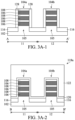
- FIGS. 3 A- 1 to 3 M- 1 illustrate cross-sectional representations of various stages of manufacturing the semiconductor structure 100 a shown along line A-A′ in FIG. 1 E and in FIG. 2 , in accordance with some embodiments.
- FIGS. 3 A- 2 to 3 M- 2 illustrate cross-sectional representations of various stages of manufacturing the semiconductor structure 100 a shown along line B-B′ in FIG. 1 E and in FIG. 2 , in accordance with some embodiments.
- FIGS. 3 A- 3 to 3 M- 3 illustrate cross-sectional representations of various stages of manufacturing the semiconductor structure 100 a shown along line C 1 -C 1 ′ and C 2 -C 2 ′ in FIG. 1 E and in FIG. 2 , in accordance with some embodiments.
- FIG. 3 A- 1 illustrates the cross-sectional representation shown along line A-A′′ in FIG. 1 E and FIG. 2 .
- FIG. 3 A- 2 illustrates the cross-sectional representation shown along line B-B′ in FIG. 1 E and FIG. 2 in accordance with some embodiments.
- FIG. 3 A- 3 illustrates the cross-sectional representation shown along line C 1 -C 1 ′ and C 2 -C 2 ′ in FIG. 1 E and in FIG. 2 .
- the source/drain (S/D) regions of the fin structure 104 are recessed to form source/drain (S/D) recesses 130 , as shown in in accordance with some embodiments. More specifically, the first semiconductor material layers 106 and the second semiconductor material layers 108 not covered by the dummy gate structures 118 and the gate spacer layers 126 are removed, in accordance with some embodiments. In addition, some portions of the base fin structure 105 are also recessed to form curved top surfaces, as shown in FIG. 3 B- 1 in accordance with some embodiments.
- the first fin structure 104 a and the second fin structure 104 b are recessed by performing an etching process.
- the etching process may be an anisotropic etching process, such as dry plasma etching, and the first dummy gate structure 118 a , the second dummy gate structure 118 b and the gate spacer layers 126 are used as etching masks during the etching process.
- the fin spacer layers 128 are also recessed to form lowered fin spacer layers 128 ′.
- the first semiconductor material layers 106 exposed by the source/drain recesses 130 are laterally recessed to form notches 132 , in accordance with some embodiments.
- an etching process is performed on the semiconductor structure 100 a to laterally recess the first semiconductor material layers 106 of the fin structure 104 from the source/drain recesses 130 .
- the first semiconductor material layers 106 have a greater etching rate (or etching amount) than the second semiconductor material layers 108 , thereby forming notches 132 between adjacent second semiconductor material layers 108 .
- the etching process is an isotropic etching such as dry chemical etching, remote plasma etching, wet chemical etching, another suitable technique, and/or a combination thereof.
- inner spacers 134 are formed in the notches 132 between the second semiconductor material layers 108 , in accordance with some embodiments.
- the inner spacers 134 are configured to separate the source/drain (S/D) structures and the gate structures formed in subsequent manufacturing processes in accordance with some embodiments.
- the inner spacers 134 are made of a dielectric material, such as silicon oxide (SiO 2 ), silicon nitride (SiN), silicon carbide (SiC), silicon oxynitride (SiON), silicon carbon nitride (SiCN), silicon oxide carbonitride (SiOCN), or a combination thereof.
- the inner spacer layer 134 is formed by a deposition process, such as chemical vapor deposition (CVD) process, atomic layer deposition (ALD) process, another applicable process, or a combination thereof.
- a hard mask layer 129 is formed on the lowered fin spacer layers 128 ′, the first fin structure 104 a , the second fin structure 104 b , and isolation structure 116 , in accordance with some embodiments.
- a photoresist layer 131 is formed over a portion of the hard mask layer 129 .
- the photoresist layer 131 is patterned to form a patterned photoresist layer 131 to transfer the pattern to the hard mask layer 129 .
- the patterned photoresist layer 131 is formed in the second sub-region 12 .
- the lowered fin spacer layers 128 ′ have a high etching selectivity with respect to the hard mask layer 129 .
- the hard mask layer 129 is made of nitride or oxide, such as silicon nitride or aluminum oxide (Al 2 O 3 ) or another applicable material.
- the hard mask layer 129 is formed by chemical vapor deposition (CVD), atomic vapor deposition (ALD), physical vapor deposition (PVD), another suitable method, or a combination thereof.
- a portion of the hard mask layer 129 in the first sub-region 11 which is not coved by the photoresist layer 131 is removed to expose the first S/D recess 130 , and then the photoresist layer 131 is removed, and a first source/drain (S/D) structure 136 a is formed in the S/D recesses 130 , in accordance with some embodiments.
- S/D source/drain
- the first source/drain (S/D) structure 136 a is formed using an epitaxial growth process, such as Molecular beam epitaxy (MBE), Metal-organic Chemical Vapor Deposition (MOCVD), Vapor-Phase Epitaxy (VPE), other applicable epitaxial growth process, or a combination thereof.
- MBE Molecular beam epitaxy
- MOCVD Metal-organic Chemical Vapor Deposition
- VPE Vapor-Phase Epitaxy
- the first source/drain (S/D) structure 136 a is made of any applicable material, such as Ge, Si, GaAs, AlGaAs, SiGe, GaAsP, SiP, SiC, SiCP, or a combination thereof.
- the first source/drain (S/D) structure 136 a is in-situ doped during the epitaxial growth process.
- the first source/drain (S/D) structure 136 a may be the epitaxially grown SiGe doped with boron (B).
- the first source/drain (S/D) structure 136 a may be the epitaxially grown Si doped with carbon to form silicon:carbon (Si:C) source/drain features, phosphorous to form silicon:phosphor (Si:P) source/drain features, or both carbon and phosphorous to form silicon carbon phosphor (SiCP) source/drain features.
- the first source/drain (S/D) structure 136 a is doped in one or more implantation processes after the epitaxial growth process.
- the hard mask layer 129 is again formed on the lowered fin spacer layers 128 ′, the isolation structure 116 and the first S/D structure 136 a , in accordance with some embodiments.
- the photoresist layer 131 is formed over a portion of the hard mask layer 129 in the first sub-region 11 , and the photoresist layer 131 is patterned to form a patterned photoresist layer 131 .
- the patterned photoresist layer 131 is in the first sub-region 11 .
- the hard mask layer 129 is removed to expose the second S/D recess 130 in the second sub-region 12 .
- the remaining hard mask layer 129 is used to protect the first S/D structure 136 a .
- the photoresist layer 131 is removed.
- a second S/D structure 136 b is formed in the second S/D recess 130 in the second sub-region 12 .
- the hard mask layer 129 is removed after the second S/D structure 136 b is formed.
- the second S/D structures 136 b is made of any applicable material, such as Ge, Si, GaAs, AlGaAs, SiGe, GaAsP, SiP, SiC, SiCP, or a combination thereof.
- the second S/D structure 136 b is formed using an epitaxial growth process, such as Molecular beam epitaxy (MBE), Metal-organic Chemical Vapor Deposition (MOCVD), Vapor-Phase Epitaxy (VPE), other applicable epitaxial growth process, or a combination thereof.
- MBE Molecular beam epitaxy
- MOCVD Metal-organic Chemical Vapor Deposition
- VPE Vapor-Phase Epitaxy
- the second S/D structure 136 b is in-situ doped during the epitaxial growth process.
- the second S/D structure 136 b may be the epitaxially grown SiGe doped with boron (B).
- the second S/D structure 136 b may be the epitaxially grown Si doped with carbon to form silicon:carbon (Si:C) source/drain features, phosphorous to form silicon:phosphor (Si:P) source/drain features, or both carbon and phosphorous to form silicon carbon phosphor (SiCP) source/drain features.
- the second S/D structures 136 b are doped in one or more implantation processes after the epitaxial growth process.
- a contact etch stop layer (CESL) 138 is conformally formed to cover the first S/D structures 136 a , the second S/D structure 136 b and an interlayer dielectric (ILD) layer 140 is formed over the contact etch stop layers 138 , in accordance with some embodiments.
- the contact etch stop layer 138 is made of a dielectric materials, such as silicon nitride, silicon oxide, silicon oxynitride, another suitable dielectric material, or a combination thereof.
- the dielectric material for the contact etch stop layers 138 may be conformally deposited over the semiconductor structure by performing chemical vapor deposition (CVD), ALD, other application methods, or a combination thereof.
- the ILD layer 140 may include multilayers made of multiple dielectric materials, such as silicon oxide, silicon nitride, silicon oxynitride, phosphosilicate glass (PSG), borophosphosilicate glass (BPSG), and/or other applicable low-k dielectric materials.
- the ILD layer 140 may be formed by chemical vapor deposition (CVD), physical vapor deposition, (PVD), atomic layer deposition (ALD), or other applicable processes.
- a planarization process such as CMP or an etch-back process may be performed until the gate electrode layers 120 of the dummy gate structures 118 are exposed, as shown in FIG. 3 I- 3 in accordance with some embodiments.
- the first dummy gate structure 118 a and the second dummy gate structure 118 b are removed to form a trench 141 , in accordance with some embodiments.
- the first fin structure 104 a and the second fin structure 104 b are exposed by the trench 141 .
- the removal process may include one or more etching processes.
- a wet etchant such as a tetramethylammonium hydroxide (TMAH) solution may be used to selectively remove the dummy gate electrode layer 122 .
- TMAH tetramethylammonium hydroxide
- the dummy gate dielectric layer 120 may be removed using a plasma dry etching, a dry chemical etching, and/or a wet etching.
- the first semiconductor material layers 106 are removed to form nanostructures 108 ′ (or channel layers 108 ′) with the second semiconductor material layers 108 , in accordance with some embodiments.
- a number of processes in FIG. 4 A- 4 C are performed on the nanostructures 108 ′.
- FIGS. 4 A to 4 C illustrate cross-sectional representations of various stages of manufacturing the semiconductor structure 100 a after the first semiconductor material layers 106 are removed, in accordance with some embodiments.
- the nanostructures 108 ′ (or channel layers 108 ′) in the first sub-region 11 and the second sub-region 12 are covered by a mask layer 133 .
- the top portion of the mask layer 133 is removed to expose the topmost nanostructures 108 ′ in the first sub-region 11 .
- the exposed topmost nanostructures 108 ′ in the first sub-region 11 is removed.
- the first S/D structure 136 a and the second S/D structure 136 b are attached to the nanostructures 108 ′.
- the first fin structure 104 a and the second fin structure 104 b include the nanostructures 108 ′.
- the first semiconductor material layers 106 may be removed by performing a selective wet etching process, such as APM (e.g., ammonia hydroxide-hydrogen peroxide-water mixture) etching process.
- APM e.g., ammonia hydroxide-hydrogen peroxide-water mixture
- the wet etching process uses etchants such as ammonium hydroxide (NH 4 OH), TMAH, ethylenediamine pyrocatechol (EDP), and/or potassium hydroxide (KOH) solutions.
- a first gate structure 142 a and a second gate structure 142 b are formed to surround the nanostructures 108 ′ and over the isolation structure 116 , in accordance with some embodiments.
- the first gate structure 142 a and the second gate structure 142 b are formed wrapped around the nanostructures 108 ′.
- the first gate structure 142 a and the second gate structure 142 b wrap around the nanostructures 108 ′ to form gate-all-around transistor structures in accordance with some embodiments.
- the first gate structure 142 a includes an interfacial layer 144 , a gate dielectric layer 146 , and a first gate electrode layer 148 a .
- the second gate structure 142 b includes an interfacial layer 144 , a gate dielectric layer 146 , and a second gate electrode layer 148 b.
- the interfacial layers 144 are oxide layers formed around the nanostructures 108 ′ and on the top of the base fin structure 105 . In some embodiments, the interfacial layers 144 are formed by performing a thermal process.
- the gate dielectric layers 146 are formed over the interfacial layers 144 , so that the nanostructures 108 ′ are surrounded (e.g. wrapped) by the gate dielectric layers 146 .
- the gate dielectric layers 146 also cover the sidewalls of the gate spacers 126 and the inner spacers 134 in accordance with some embodiments.
- the gate dielectric layers 146 are made of one or more layers of dielectric materials, such as HfO 2 , HfSiO, HfSiON, HfTaO, HfTiO, HfZrO, zirconium oxide, aluminum oxide, titanium oxide, hafnium dioxide-alumina (HfO 2 —Al 2 O 3 ) alloy, another suitable high-k dielectric material, or a combination thereof.
- the gate dielectric layers 146 are formed using chemical vapor deposition (CVD), atomic layer deposition (ALD), another applicable method, or a combination thereof.
- the first gate structure 142 a and the second gate structure 142 b are formed on the gate dielectric layer 146 .
- the first gate structure 142 a and the second gate structure 142 b are made of one or more layers of conductive material, such as aluminum, copper, titanium, tantalum, tungsten, cobalt, molybdenum, tantalum nitride, nickel silicide, cobalt silicide, TiN, WN, TiAl, TiAlN, TaCN, TaC, TaSiN, metal alloys, another suitable material, or a combination thereof.
- the first gate structure 142 a and the second gate structure 142 b are formed using chemical vapor deposition (CVD), atomic layer deposition (ALD), electroplating, another applicable method, or a combination thereof.
- CVD chemical vapor deposition
- ALD atomic layer deposition
- electroplating another applicable method, or a combination thereof.
- Other conductive layers, such as work function metal layers, may also be formed in the first gate structure 142 a and the second gate structure 142 b , although they are not shown in the figures.
- the n-work function layer includes tungsten (W), copper (Cu), titanium (Ti), silver (Ag), aluminum (Al), titanium nitride (TiN), tantalum nitride (TaN), tantalum carbide (TaC), titanium aluminum alloy (TiAl), titanium aluminum nitride (TiAlN), tantalum carbon nitride (TaCN), tantalum silicon nitride (TaSiN), manganese (Mn), zirconium (Zr) or a combination thereof.
- the p-work function layer includes titanium (Ti), titanium nitride (TiN), tantalum nitride (TaN), tantalum carbide (TaC), molybdenum nitride, tungsten nitride (WN), ruthenium (Ru) or a combination thereof.
- a planarization process such as CMP or an etch-back process may be performed until the ILD layer 140 is exposed.
- an etch stop layer 150 is formed over the gate structure 142 , and a dielectric layer 152 is formed over the etch stop layer 150 , in accordance with some embodiments.
- the etch stop layer 150 is made of a dielectric materials, such as silicon nitride, silicon oxide, silicon oxynitride, another suitable dielectric material, or a combination thereof.
- the dielectric material for the etch stop layers 150 may be conformally deposited over the semiconductor structure by performing chemical vapor deposition (CVD), ALD, other application methods, or a combination thereof.
- the dielectric layer 152 may include multilayers made of multiple dielectric materials, such as silicon oxide, silicon nitride, silicon oxynitride, phosphosilicate glass (PSG), borophosphosilicate glass (BPSG), and/or other applicable low-k dielectric materials.
- the dielectric layer 152 may be formed by chemical vapor deposition (CVD), physical vapor deposition, (PVD), atomic layer deposition (ALD), or other applicable processes.
- a silicide layer 154 and an S/D contact structure 156 are formed over the first S/D structure 136 a and the second S/D structure 136 b , in accordance with some embodiments.
- the contact openings may be formed through the contact etch stop layer 138 , the interlayer dielectric layer 140 , the etch stop layer 150 and the dielectric layer 152 to expose the top surfaces of the first S/D structures 136 a and the second S/D structure 136 b , and then the silicide layers 154 and the S/D contact structure 156 may be formed in the contact openings.
- the contact openings may be formed using a photolithography process and an etching process.
- some portions of the first S/D structure 136 a and second S/D structure 136 b exposed by the contact openings may also be etched during the etching process.
- the silicide layers 154 may be formed by forming a metal layer over the top surfaces of the first S/D structure 136 a and the second S/D structure 136 b and annealing the metal layer so the metal layer reacts with the first S/D structure 136 a and the second S/D structure 136 b to form the silicide layers 154 .
- the unreacted metal layer may be removed after the silicide layers 154 are formed.
- the S/D contact structure 156 may include a barrier layer and a conductive layer. In some other embodiments, the S/D contact structure 156 does not include a barrier layer.
- the barrier layer is made of titanium (Ti), titanium nitride (TiN), tantalum (Ta), tantalum nitride (TaN), or another applicable material.
- the barrier layer is formed by using a process such as chemical vapor deposition (CVD), physical vapor deposition (PVD), plasma enhanced CVD (PECVD), plasma enhanced physical vapor deposition (PEPVD), atomic layer deposition (ALD), or any other applicable deposition processes.
- the conductive layer is made of tungsten (W), ruthenium (Ru), molybdenum (Mo), or the like.
- the conductive layer is formed by performing a deposition process, such as chemical vapor deposition (CVD), physical vapor deposition, (PVD), atomic layer deposition (ALD), or other applicable processes.
- CVD chemical vapor deposition
- PVD physical vapor deposition
- ALD atomic layer deposition
- an etch stop layer 162 is formed over the S/D contact structure 156 , and a dielectric layer 164 is formed over the etch stop layer 162 , in accordance with some embodiments.
- an S/D conductive via 166 is formed over the S/D contact structure 156 , and a gate conductive plug 168 is formed over the first gate structure 142 a and the second gate structure 142 b.
- the etch stop layer 162 is made of a dielectric materials, such as silicon nitride, silicon oxide, silicon oxynitride, another suitable dielectric material, or a combination thereof.
- the dielectric material for the contact etch stop layers 162 may be conformally deposited over the semiconductor structure by performing chemical vapor deposition (CVD), atomic layer deposition (ALD), other application methods, or a combination thereof.
- the dielectric layer 164 may include multilayers made of multiple dielectric materials, such as silicon oxide, silicon nitride, silicon oxynitride, phosphosilicate glass (PSG), borophosphosilicate glass (BPSG), and/or other applicable low-k dielectric materials.
- the dielectric layer 164 may be formed by chemical vapor deposition (CVD), physical vapor deposition, (PVD), atomic layer deposition (ALD), or other applicable processes.
- the S/D conductive via 166 is made of conductive material, such as tungsten (W), ruthenium (Ru), molybdenum (Mo), or the like.
- the S/D conductive via 166 is formed by performing a deposition process, such as chemical vapor deposition (CVD), physical vapor deposition, (PVD), atomic layer deposition (ALD), or other applicable processes.
- CVD chemical vapor deposition
- PVD physical vapor deposition
- ALD atomic layer deposition
- the gate conductive plug 168 is made of conductive material, such as tungsten (W), ruthenium (Ru), molybdenum (Mo), or the like.
- the gate conductive plug 168 is formed by performing a deposition process, such as chemical vapor deposition (CVD), physical vapor deposition, (PVD), atomic layer deposition (ALD), or other applicable processes.
- CVD chemical vapor deposition
- PVD physical vapor deposition
- ALD atomic layer deposition
- the number of nanostructures 108 ′ (or channel layers 108 ′) directly below in the second gate structure 142 b - 1 in first sub-region 11 become two, and the number of nanostructures 108 ′ (or channel layers 108 ′) directly below the second gate structure 142 b - 2 in the second sub-region 12 is still three. More specifically, the number of nanostructures 108 ′ (or channel layers 108 ′) directly below the second gate structure 142 b - 1 in the first sub-region 11 is two, and the number of nanostructures 108 ′ (or channel layers 108 ′) directly below the gate spacer layer 126 in the first sub-region 11 is three.
- the number of nanostructures 108 ′ (or channel layers 108 ′) directly below in the second gate structure 142 b - 2 in second sub-region 12 is three. Therefore, the number of nanostructures 108 ′ (or channel layers 108 ′) directly below the second gate structure 142 b - 1 in the first sub-region 11 is smaller than the number of nanostructures 108 ′ (or channel layers 108 ′) directly below in the second gate structure 142 b - 2 in second sub-region 12 .
- the second gate structure 142 b - 1 has a continuous sidewall surface in direct contact with the gate spacer layer 126 , and the bottom surface of the continuous sidewall surface of the second gate structure 142 b - 1 is lower than the bottom surface of the gate spacer layer 126 .
- the continuous sidewall surface of the second gate structure 142 b - 1 is in direct contact with the topmost nanostructure 108 a′.
- the topmost nanostructure is divided into two portions by the second gate structure 142 b - 1 , and the two portions of the first gate structure 142 a are in direct contact with the gate spacer layer 126 .
- More nanostructures can provide large effective width (W eff ) of the channel layer.
- the large effective width (W eff ) of channel layer can provide high speed of the semiconductor structure 100 a .
- the larger effective width of the channel layer consumes more power.
- larger effective width (W eff ) is formed by having more nanostructures.
- a smaller effective width (W eff ) is formed by having fewer nanostructures.
- the second gate structure 142 b - 1 in the first sub-region 11 is formed for power efficiency
- the second gate structure 142 b - 2 in the second sub-region 12 is formed for high speed performance.
- the second gate structure 142 b - 1 and second gate structure 142 b - 2 co-exist to achieve multi-nanostructures for speed performance and power efficiency.
- the second area of the S/D contact structure 156 in the second sub-region 12 is greater than the first area of the S/D contact structure 156 in the first sub-region 11 .
- the area ratio of the second area of the S/D contact structure 156 to the first area of the S/D contact structure 156 is in a range from about 1.1 to about 2.5.
- the second area of the S/D conductive via structure 166 in the second sub-region 12 is greater than the first area of the S/D conductive via structure 166 in the first sub-region 11 .
- the area ratio of the second area of the S/D conductive via structure 166 to the first area of the S/D conductive via structure 166 is in a range from about 1.1 to about 2.5.
- FIG. 5 illustrates a cross-sectional view of a semiconductor structure 100 b , in accordance with some embodiments.
- the semiconductor structure 100 b of FIG. 5 includes elements that are similar to, or the same as, elements of the semiconductor structure 100 a of FIG. 3 M- 3 .
- the difference between FIG. 5 and FIG. 3 M- 3 is that there is a bottom isolation layer 135 below the first source/drain (S/D) structure 136 a and the second S/D structure 136 b .
- the bottom isolation layer 135 is used to reduce leakage from the semiconductor structure 100 a.
- the bottom isolation layer 135 includes un-doped Si, un-doped SiGe or a combination thereof.
- the bottom isolation layer 135 is formed by an epitaxy or epitaxial (epi) process.
- the epi process may include a selective epitaxial growth (SEG) process, CVD deposition techniques (e.g., vapor-phase epitaxy (VPE) and/or ultra-high vacuum CVD (UHV-CVD)), molecular beam epitaxy, or other suitable epi processes.
- SEG selective epitaxial growth
- CVD deposition techniques e.g., vapor-phase epitaxy (VPE) and/or ultra-high vacuum CVD (UHV-CVD)
- molecular beam epitaxy or other suitable epi processes.
- FIG. 6 shows a top-view representation of a semiconductor structure 100 c , in accordance with some embodiments.
- the substrate 102 includes the first region 10 , a second region 20 , a third region 30 and a fourth region 40 .
- the first region 10 includes the first sub-region 11 and a second sub-region 12 (shown in FIG. 2 ).
- the third region 30 is between the second region 20 and the fourth region 40 , and the third region 30 is adjacent to the first region 10 .
- a third fin structure 104 c is formed along the first direction (e.g. X-axis).
- the first fin structure 104 a , the second fin structure 104 b and the third fin structure 104 c are parallel to each other.
- the third fin structure 104 c is adjacent to the second fin structure 104 b , and the second fin structure 104 b is between the first fin structure 104 a and the third fin structure 104 c .
- the third fin structure 104 c has different widths in different regions along the second direction (e.g. y-axis).
- the third fin structure 104 c has a first width W 1 in the second region 20 , a second width W 2 in the third region 30 and a third width W 3 in the fourth region 40 .
- the first width W 1 is smaller than the second width W 2
- the second width W 2 is smaller than the third width W 3 .
- a third gate structure 142 c is formed across the third fin structure 104 c .
- the first gate structure 142 a and the second gate structure 142 b are formed across the third fin structure 104 c .
- the fourth gate structure 142 d is formed across the third fin structure 104 c.
- a first dielectric structure 145 a is formed between the second region 20 and the third region 30
- a second dielectric structure 145 b is formed between the third region 30 and the fourth region 40 .
- the first dielectric structure 145 a is in parallel to the third gate structure 142 c .
- the second dielectric structure 145 b is also in parallel to the third gate structure 142 c .
- the first dielectric structure 145 a and the second dielectric structure 145 b are used to reduce leakage from two adjacent semiconductor devices.
- FIGS. 7 A to 7 C illustrate cross-sectional representations of various stages of manufacturing the semiconductor structure 100 c shown along line B 1 -B 1 ′, B 2 -B 2 ′ and B 3 -B 3 ′ in FIG. 6 , in accordance with some embodiments.
- the semiconductor structure 100 c of FIGS. 7 A- 7 C includes elements that are similar to, or the same as, elements of the semiconductor structure 100 a of FIGS. 3 A- 1 to 3 M- 1 , 3 A- 2 to 3 M- 2 and 3 A- 3 to 3 M- 3 .
- FIG. 7 A there are two nanostructures 108 ′ (or channel layers 108 ′) in the second region 20 , there are three nanostructures 108 ′ in the third region 30 and there are fourth nanostructures 108 ′′ in the fourth region 40 .
- the formation of the nanostructures 108 ′ (or channel layers 108 ′) is described in FIGS. 3 A- 2 to 3 M- 2 , and the detail is not described again for brevity.
- the numbers of the nanostructures 108 ′ in the second region 20 , that in the third region 30 and that in the fourth region 40 are the same in original design, but after the processes (e.g. FIGS. 4 A- 4 C ), the number of nanostructures 108 ′ in the second region 20 becomes two and the number of nanostructures 108 ′ in the third region 30 become three.
- the number of nanostructures 108 ′ (or channel layers 108 ′) in the second region 20 is smaller than the number of nanostructures 108 ′ (or channel layers 108 ′) in the third region 30 .
- the number of nanostructures 108 ′ (or channel layers 108 ′) in the third region 30 is smaller than the nanostructures 108 ′ (or channel layers 108 ′) in the fourth region 40 .
- the nanostructures 108 ′ (or channel layers 108 ′) has the first width W 1 .
- the nanostructures 108 ′ (or channel layers 108 ′) has the second width W 2 .
- the nanostructures 108 ′ (or channel layers 108 ′) has the third width W 3 .
- the first width W 1 is smaller than the second width W 2
- the second width W 2 is smaller than the third width W 3 .
- the third gate structure 142 c is formed to surround the nanostructures 108 ′ (or channel layers 108 ′) in the second region 20 , in accordance with some embodiments.
- the first gate structure 142 a and the second gate structure 142 b is formed to surround the nanostructures 108 ′ (or channel layers 108 ′) in the third region 30
- the fourth gate structure 142 d is formed to surround the nanostructures 108 ′ (or channel layers 108 ′) in the fourth region 40 .
- the first width W 1 of the nanostructures 108 ′ (or channel layers 108 ′) directly below the third gate structure 142 c in the second region 20 is smaller than the second width W 2 of the nanostructures 108 ′ (or channel layers 108 ′) directly below the second gate structure 142 b in the third region 30 .
- the second width W 2 of the nanostructures 108 ′ (or channel layers 108 ′) directly below the first gate structure 142 a in the third region 30 is smaller than third width W 3 of the fourth gate structure 142 d in the fourth region 40 .
- the etching stop layer 150 and the dielectric layer 152 is formed over the third gate structure 142 c , the first gate structure 142 a , the second gate structure 142 b and the fourth gate structure 142 d.
- the etching stop layer 162 and the dielectric layer 164 are formed over the dielectric layer 152 .
- the S/D conductive via structure 166 (not shown) is formed through the dielectric layer 164 and the etching stop layer 162 .
- the gate contact structure 168 is formed through the dielectric layer 164 , the etching stop layer 162 , the dielectric layer 152 and the etching stop layer 150 .
- the gate contact structure 168 is connected to the third gate structure 142 c in the second region 20 , the first gate structure 142 a in the third region 30 and the fourth gate structure 142 d in the fourth region 40 .
- FIG. 8 illustrates a perspective view of a semiconductor structure 100 d , in accordance with some embodiments.
- the semiconductor structure 100 d of FIG. 8 includes elements that are similar to, or the same as, elements of the semiconductor structure 100 a of FIG. 1 E .
- the difference between FIG. 8 and FIG. 1 E is that there is a third dummy gate structure 118 c between the first dummy gate structure 118 a and the second dummy gate structure 118 b.
- FIG. 9 shows a top-view representation of the semiconductor structure 100 d , in accordance with some embodiments.
- the first fin structure 104 a and the second fin structure 104 b are parallel to each other, and the first dummy gate structure 118 a , the second dummy gate structure 118 b and the third dummy gate structure 118 c are formed across the first fin structure 104 a and the second fin structure 104 b .
- the third dummy gate structure 118 c will be replaced by the dielectric structure 145 (shown in FIG. 10 E- 3 ).
- the dielectric structure 145 is an isolation structure to reduce the leakage.
- the first fin structure 104 a has a fourth width W 4 on the left side of the third dummy gate structure 118 c and a fifth width W 5 on the right side of the third dummy gate structure 118 c .
- the fourth width W 4 and the fifth width W 5 are along the second direction (e.g. y-direction). In some embodiments, the fourth width W 4 is smaller than the fifth width W 5 .
- FIGS. 10 A- 1 to 10 F- 1 illustrate cross-sectional representations of various stages of manufacturing the semiconductor structure 100 d shown along line A-A′ in FIG. 8 and in FIG. 9 , in accordance with some embodiments.
- FIGS. 10 A- 2 to 10 D- 2 illustrate cross-sectional representations of various stages of manufacturing the semiconductor structure 100 d shown along line B-B′ in FIG. 8 and in FIG. 9 , in accordance with some embodiments.
- FIGS. 10 E- 2 to 10 F- 2 illustrate cross-sectional representations of various stages of manufacturing the semiconductor structure 100 d shown along line B-B′ and F-F′ in FIG. 8 and in FIG. 9 , in accordance with some embodiments.
- FIGS. 10 A- 3 to 10 B- 3 illustrate cross-sectional representations of various stages of manufacturing the semiconductor structure 100 d shown along line D 1 -D 1 ′ in FIG. 8 and in FIG. 9 , in accordance with some embodiments.
- FIGS. 10 C- 3 to 10 D- 3 illustrate cross-sectional representations of various stages of manufacturing the semiconductor structure 100 d shown along line D 2 -D 2 ′ in FIG. 8 and in FIG. 9 , in accordance with some embodiments.
- FIGS. 10 E- 3 to 10 F- 3 illustrate cross-sectional representations of various stages of manufacturing the semiconductor structure 100 d shown along line C-C′, D 1 -D 1 ′ and E-E′ in FIG. 8 and in FIG. 9 , in accordance with some embodiments.
- the semiconductor structure 100 d of FIGS. 10 A- 1 to 10 F- 1 , 10 A- 2 to 10 F- 2 , and 10 A- 3 to 10 F- 3 includes elements that are similar to, or the same as, elements of the semiconductor structure 100 a of FIGS. 3 A- 1 to 3 M- 1 , 3 A- 2 to 3 M- 2 and 3 A- 3 to 3 M- 3 .
- the first S/D structure 136 a - 1 is formed in the S/D recesses 130 , in accordance with some embodiments.
- the first S/D structure 136 a - 1 is formed on right side of the third dummy gate structure 118 c , and a mask layer 137 is formed on the left side of the third dummy gate structure 118 c.
- the first source/drain (S/D) structure 136 a - 1 is formed using an epitaxial growth process, such as Molecular beam epitaxy (MBE), Metal-organic Chemical Vapor Deposition (MOCVD), Vapor-Phase Epitaxy (VPE), other applicable epitaxial growth process, or a combination thereof.
- the first source/drain (S/D) structure 136 a - 1 is made of any applicable material, such as Ge, Si, GaAs, AlGaAs, SiGe, GaAsP, SiP, SiC, SiCP, or a combination thereof.
- the mask layer 137 is removed, and the first S/D structure 136 a - 2 is formed in the S/D recess 130 at the left side of the third dummy gate structure 118 c , in accordance with some embodiments.
- the top surface of the first S/D structure 136 a - 2 at the left side of the third dummy gate structure 118 c is lower than the top surface of the first S/D structure 136 a - 1 at the right side of the third dummy gate structure 118 c .
- the top surface of the first S/D structure 136 a - 2 is lower than the topmost second semiconductor material layer 108 .
- the second S/D structure 136 b - 1 is formed adjacent to the first S/D structure 136 a - 1 , in accordance with some embodiments.
- the second S/D structure 136 b - 1 is formed on right side of the third dummy gate structure 118 c
- the mask layer 137 is formed on the left side of the third dummy gate structure 118 c .
- the second S/D structure 136 b - 1 and the first S/D structure 136 a - 1 are made of different materials.
- the second source/drain (S/D) structure 136 b - 1 is formed using an epitaxial growth process, such as Molecular beam epitaxy (MBE), Metal-organic Chemical Vapor Deposition (MOCVD), Vapor-Phase Epitaxy (VPE), other applicable epitaxial growth process, or a combination thereof.
- the second source/drain (S/D) structure 136 b - 1 is made of any applicable material, such as Ge, Si, GaAs, AlGaAs, SiGe, GaAsP, SiP, SiC, SiCP, or a combination thereof.
- the mask layer 137 is removed, and the second S/D structure 136 b - 2 is formed in the S/D recess 130 at the left side of the third dummy gate structure 118 c , in accordance with some embodiments.
- the top surface of the second S/D structure 136 b - 2 at the left side of the third dummy gate structure 118 c is lower than the top surface of the second S/D structure 136 b - 1 at the right side of the third dummy gate structure 118 c .
- the top surface of the second S/D structure 136 b - 2 is lower than the topmost second semiconductor material layer 108 .
- the first gate structure 142 a , the dielectric structure 145 and the second gate structure 142 b are formed across the first fin structure 104 a and the second fin structure 104 b , in accordance with some embodiments.
- the dielectric structure 145 is between the first gate structure 142 a and the second gate structure 142 b.
- the dielectric structure 145 is formed by following processes.
- the third dummy gate structure 118 c , and the first semiconductor material layers 106 and the second semiconductor material layer 108 are removed to form a trench and a dielectric material is filled into the trench to form the dielectric structure 145 .
- the bottom surface of the dielectric structure 145 is lower than the bottom surface of first S/D structure 136 a - 1 and 136 a - 2 .
- the dielectric structure 145 is in direct contact with the inner spacer layer 134 and the gate spacer layer 126 .
- FIG. 10 E- 2 illustrate cross-sectional representation of the semiconductor structure 100 d shown along line B-B′ and F-F′ in FIG. 8 and in FIG. 9 , in accordance with some embodiments.
- the fourth width W 4 of the nanostructures 108 ′ along the second direction (e.g. y-axis) directly below the first gate structure 142 a is smaller than the fifth width W 5 of the nanostructures 108 ′ along the second direction (e.g. y-axis) directly below the second gate structure 142 b.
- FIG. 10 E- 3 illustrate cross-sectional representation of the semiconductor structure 100 d shown along line C-C′, D 1 -D 1 ′ and E-E′ in FIG. 8 and in FIG. 9 , in accordance with some embodiments.
- the first dummy gate structure 118 a is replaced with the first gate structure 142 a
- the third dummy gate structure 118 c is replaced with the dielectric structure 145
- the second dummy gate structure 118 b is replaced with the second gate structure 142 b.
- the first S/D structure 136 a - 2 is one the left side of the first gate structure 142 a and the first S/D structure 136 a - 2 is on the right side of the first gate structure 142 a.
- the first S/D structure 136 a - 2 is one the left side of the first gate structure 142 a and the first S/D structure 136 a - 1 is on the right side of the dielectric structure 145 .
- first S/D structure 136 a - 1 is one the left side of the second gate structure 142 b and the first S/D structure 136 a - 1 is on the right side of the second gate structure 142 b .
- the top surface of first S/D structure 136 a - 1 is higher than the top surface of first S/D structure 136 a - 2 .
- the first S/D structure 136 a - 1 has a third depth D 3
- the first S/D structure 136 a - 2 has a fourth depth D 4 .
- the third depth D 3 is greater than the fourth depth D 4 .
- the topmost nanostructure 108 ′ is divided into two portions by the first gate structure 142 a , and the two portions of the first gate structure 142 a are in direct contact with the gate spacer layer 126 .
- the first gate structure 142 a has a continuous sidewall surface in direct contact with the gate spacer layer 126 , and the continuous sidewall surface of the first gate structure 142 a is in direct contact with the topmost nanostructure 108 ′.
- the etching stop layer 150 and the dielectric layer 152 are formed over the first gate structure 142 a , the dielectric structure 145 and the second gate structure 142 b .
- the S/D contact structure 156 is formed through the dielectric layer 152 , the etching stop layer 150 and the dielectric layer 140 .
- the etching stop layer 162 and the dielectric layer 164 are formed over the dielectric layer 152 .
- the S/D conductive via structure 166 is formed through the dielectric layer 164 and the etching stop layer 162 .
- the gate contact structure 168 is formed through the dielectric layer 164 , the etching stop layer 162 , the dielectric layer 152 and the etching stop layer 150 .
- the gate contact structure 168 is connected to the first gate structure 142 a and the second gate structure 142 b.
- the number of nanostructures 108 ′ directly below the first gate structure 142 a is smaller than the number of nanostructures 108 ′ directly below the second gate structure 142 b.
- the topmost surface of the inner spacer layer 134 is higher than the top surface of the first S/D structure 136 a - 2 .
- the topmost surface of the inner spacer layer 134 is higher than the bottom surface of S/D contact structure 156 .
- the top surface of the first S/D structure 136 a - 2 is lower than the top surface of the topmost nanostructures 108 ′ (channel layer 108 ′).
- the top surface of the first S/D structure 136 a - 1 in direct contact with three nanostructures 108 ′ is higher than the top surface of the first S/D structure 136 a - 2 in direct contact with two nanostructures 108 ′.
- FIG. 11 illustrates a cross-sectional view of a semiconductor structure 100 e , in accordance with some embodiments.
- the semiconductor structure 100 e of FIG. 11 includes elements that are similar to, or the same as, elements of the semiconductor structure 100 d of FIG. 10 F- 3 .
- the difference between FIG. 11 and FIG. 10 F- 3 is that there is a bottom isolation layer 135 below the first source/drain (S/D) structure 136 a - 1 and the first S/D structure 136 a - 2 .
- the bottom isolation layer 135 is used to reduce leakage from the semiconductor structure 100 a.
- the bottom isolation layer 135 includes un-doped Si, un-doped SiGe or a combination thereof.
- the bottom isolation layer 135 is formed by an epitaxy or epitaxial (epi) process.
- the epi process may include a selective epitaxial growth (SEG) process, CVD deposition techniques (e.g., vapor-phase epitaxy (VPE) and/or ultra-high vacuum CVD (UHV-CVD)), molecular beam epitaxy, or other suitable epi processes.
- SEG selective epitaxial growth
- CVD deposition techniques e.g., vapor-phase epitaxy (VPE) and/or ultra-high vacuum CVD (UHV-CVD)
- molecular beam epitaxy or other suitable epi processes.
- FIGS. 12 A- 1 to 12 B- 1 illustrate cross-sectional representations of various stages of manufacturing a semiconductor structure 100 f shown along line A-A′ in FIG. 8 and in FIG. 9 , in accordance with some embodiments.
- FIGS. 12 A- 2 to 12 B- 2 illustrate cross-sectional representations of various stages of manufacturing the semiconductor structure 100 f shown along line B-B′ in FIG. 8 and in FIG. 9 , in accordance with some embodiments.
- FIGS. 12 A- 3 to 12 B- 3 illustrate cross-sectional representations of various stages of manufacturing the semiconductor structure 100 f shown along line C-C′ and E-E′ in FIG. 8 and in FIG. 9 , in accordance with some embodiments.
- FIGS. 12 A- 1 and 12 A- 2 includes elements that are similar to, or the same as, elements of the semiconductor structure 100 a of FIGS. 3 L- 1 and 3 L- 2 .
- the top surface of the second gate structure 142 b is substantially leveled with the top surface of the gate spacer layer 126 shown along line E-E′ in FIG. 8 and in FIG. 9 .
- the top surface of the first gate structure 142 a is lower than the top surface of the gate spacer layer 126 shown along line C-C′ in FIG. 8 and in FIG. 9 .
- the top surface of the first gate structure 142 a is lower than the top surface of the second gate structure 142 b .
- the top portion of the first gate structure 142 a which is in direct contact with the gate spacer layer 126 has a first height H 1 .
- the top portion of the second gate structure 142 b which is in direct contact with the gate spacer layer 126 has a second height H 2 .
- the first height H 1 is smaller than the second height H 2 .
- the top portion of the first gate structure 142 a is removed to form a recess (not shown), and the mask layer 143 is filled into the recess. Note that the number of nanostructures 108 ′ (or channel layers) directly below the first gate structure 142 a is smaller than the number of nanostructures 108 ′ (or channel layers) directly below the second gate structure 142 b.
- FIG. 13 illustrates a cross-sectional view of a semiconductor structure 100 g , in accordance with some embodiments.
- the semiconductor structure 100 g of FIG. 13 includes elements that are similar to, or the same as, elements of the semiconductor structure 100 f of FIG. 12 B- 3 .
- the difference between FIG. 13 and FIG. 12 B- 3 is that there is a bottom isolation layer 135 below the first source/drain (S/D) structure 136 a .
- the bottom isolation layer 135 is used to reduce leakage from the semiconductor structure 100 a.
- the bottom isolation layer 135 includes un-doped Si, un-doped SiGe or a combination thereof.
- the bottom isolation layer 135 is formed by an epitaxy or epitaxial (epi) process.
- the epi process may include a selective epitaxial growth (SEG) process, CVD deposition techniques (e.g., vapor-phase epitaxy (VPE) and/or ultra-high vacuum CVD (UHV-CVD)), molecular beam epitaxy, or other suitable epi processes.
- SEG selective epitaxial growth
- CVD deposition techniques e.g., vapor-phase epitaxy (VPE) and/or ultra-high vacuum CVD (UHV-CVD)
- molecular beam epitaxy or other suitable epi processes.
- semiconductor structures 100 a to 100 g having different number of nanostructures 108 ′ (or channel layers) in different regions for performing different functions described above may also be applied to FinFET structures, although this is not shown in the figures.
- FIGS. 1 A to 13 may be designated by the same numerals and may include similar or the same materials and may be formed by similar or the same processes; therefore such redundant details are omitted in the interest of brevity.
- FIGS. 1 A to 13 are described in relation to the method, it will be appreciated that the structures disclosed in FIGS. 1 A to 13 are not limited to the method but may stand alone as structures independent of the method. Similarly, although the methods shown in FIGS. 1 A to 13 are not limited to the disclosed structures but may stand alone independent of the structures.
- the nanostructures described above may include nanowires, nanosheets, or other applicable nanostructures in accordance with some embodiments.
- Embodiments for forming semiconductor structures may be provided.
- the semiconductor structure includes a first fin structure and a second fin structure formed over a substrate.
- the first fin structure includes first nanostructures
- the second fin structure includes second nanostructures along a first direction (e.g. x-axis).
- a first gate structure formed over the first nanostructures and a first S/D structure adjacent to the first gate structure.
- a second gate structure formed over the second nanostructures along the second direction (e.g. y-axis).
- a gate spacer layer is adjacent to the gate structure. A portion of the topmost nanostructures is removed, and therefore the number of nanostructures directly below and surrounded by the gate structure is reduced.
- the first width of the first nanostructures along the second direction is smaller than the second width of the second nanostructures along the second direction.
- the first gate structure is formed for power efficiency
- the second gate structure is formed for high speed performance.
- the first gate structure and second gate structure co-exist to achieve multi-nanostructures for speed performance and power efficiency. Therefore, the performance of the semiconductor structure is improved.
- a semiconductor structure in some embodiments, includes first nanostructures formed over a substrate along a first direction, and a first gate structure formed over the first nanostructures along a second direction.
- the semiconductor structure includes a gate spacer layer formed adjacent to the first gate structure, and a first number of the first nanostructures directly below the gate spacer layer is greater than a second number of the nanostructures directly below the first gate structure.
- a semiconductor structure in some embodiments, includes first channel layers formed over a first region of a substrate along a first direction.
- the semiconductor structure includes second channel layers adjacent to the first channel layers and over a second region of the substrate.
- the semiconductor structure includes a first gate structure formed over the first fin structure along a second direction, and a topmost first channel layer is divided into two portions by the first gate structure.
- the semiconductor structure includes a second gate structure formed over the second fin structure along the second direction, and a first number of the first channel layers directly below the first gate structure is smaller than a second number of the second channel layers directly below the second gate structure.
- a method for forming a semiconductor structure includes forming a first fin structure and a second fin structure over a first region and a second region of a substrate, respectively, and the first fin structure includes first semiconductor material layers and second semiconductor material layers alternately stacked, and the second fin structure includes first semiconductor material layers and second semiconductor material layers alternately stacked.
- the method includes forming a first dummy gate structure and a second dummy gate structure over the first fin structure and the second fin structure, and forming a first gate spacer layer adjacent to the first dummy gate structure.
- the method also includes removing the first dummy gate structure and the second dummy gate structure to expose the first fin structure and the second fin structure.
- the method further includes removing all of the second semiconductor material layers to expose the first semiconductor material layers.
- the method includes removing a portion of a topmost first semiconductor material layer in the first region directly below the first dummy gate structure, and another portion of the topmost first semiconductor material layer in the first region directly below the first gate spacer layer is not removed, wherein a first number of the first semiconductor material layers directly below the first gate spacer layer is greater than a second number of the first semiconductor material layers directly below the first gate structure.
Landscapes
- Insulated Gate Type Field-Effect Transistor (AREA)
Abstract
Description
- The electronics industry is experiencing ever-increasing demand for smaller and faster electronic devices that are able to perform a greater number of increasingly complex and sophisticated functions. Accordingly, there is a continuing trend in the semiconductor industry to manufacture low-cost, high-performance, and low-power integrated circuits (ICs). So far, these goals have been achieved in large part by scaling down semiconductor IC dimensions (e.g., minimum feature size) and thereby improving production efficiency and lowering associated costs. However, such miniaturization has introduced greater complexity into the semiconductor manufacturing process. Thus, the realization of continued advances in semiconductor ICs and devices calls for similar advances in semiconductor manufacturing processes and technology.
- Recently, multi-gate devices have been introduced in an effort to improve gate control by increasing gate-channel coupling, reduce OFF-state current, and reduce short-channel effects (SCEs). However, integration of fabrication of the multi-gate devices can be challenging.
- Aspects of the present disclosure are best understood from the following detailed description when read with the accompanying Figures. It should be noted that, in accordance with the standard practice in the industry, various features are not drawn to scale. In fact, the dimensions of the various features may be arbitrarily increased or reduced for clarity of discussion.
-
FIGS. 1A to 1E illustrate perspective views of intermediate stages of manufacturing a semiconductor structure in accordance with some embodiments. -
FIG. 2 shows a top-view representation of the semiconductor structure, in accordance with some embodiments. -
FIGS. 3A-1 to 3M-1 illustrate cross-sectional representations of various stages of manufacturing the semiconductor structure shown along line A-A′ inFIG. 1E and inFIG. 2 , in accordance with some embodiments. -
FIGS. 3A-2 to 3M-2 illustrate cross-sectional representations of various stages of manufacturing the semiconductor structure shown along line B-B′ inFIG. 1E and inFIG. 2 , in accordance with some embodiments. -
FIGS. 3A-3 to 3M-3 illustrate cross-sectional representations of various stages of manufacturing the semiconductor structure shown along line C1-C1′ and C2-C2′ inFIG. 1E and inFIG. 2 , in accordance with some embodiments. -
FIGS. 4A to 4C illustrate cross-sectional representations of various stages of manufacturing the semiconductor structure after the first semiconductor material layers are removed, in accordance with some embodiments. -
FIG. 5 illustrates a cross-sectional view of a semiconductor structure, in accordance with some embodiments. -
FIG. 6 shows a top-view representation of a semiconductor structure, in accordance with some embodiments. -
FIGS. 7A to 7C illustrate cross-sectional representations of various stages of manufacturing the semiconductor structure shown along line B1-B1′, B2-B2′ and B3-B3′ inFIG. 6 , in accordance with some embodiments. -
FIG. 8 illustrates a perspective view of a semiconductor structure, in accordance with some embodiments -
FIG. 9 shows a top-view representation of the semiconductor structure, in accordance with some embodiments. -
FIGS. 10A-1 to 10F-1 illustrate cross-sectional representations of various stages of manufacturing thesemiconductor structure 100 d shown along line A-A′ inFIG. 8 and inFIG. 9 , in accordance with some embodiments. -
FIGS. 10A-2 to 10D-2 illustrate cross-sectional representations of various stages of manufacturing thesemiconductor structure 100 d shown along line B-B′ inFIG. 8 and inFIG. 9 , in accordance with some embodiments. -
FIGS. 10E-2 to 10F-2 illustrate cross-sectional representations of various stages of manufacturing thesemiconductor structure 100 d shown along line B-B′ and F-F′ inFIG. 8 and inFIG. 9 , in accordance with some embodiments. -
FIGS. 10A-3 to 10B-3 illustrate cross-sectional representations of various stages of manufacturing the semiconductor structure shown along line D1-D1′ inFIG. 8 and inFIG. 9 , in accordance with some embodiments. -
FIGS. 10C-3 to 10D-3 illustrate cross-sectional representations of various stages of manufacturing the semiconductor structure shown along line D2-D2′ inFIG. 8 and inFIG. 9 , in accordance with some embodiments. -
FIGS. 10E-3 to 10F-3 illustrate cross-sectional representations of various stages of manufacturing the semiconductor structure shown along line C-C′, D1-D1′ and E-E′ inFIG. 8 and inFIG. 9 , in accordance with some embodiments. -
FIG. 11 illustrates a cross-sectional view of a semiconductor structure, in accordance with some embodiments. -
FIGS. 12A-1 to 12B-1 illustrate cross-sectional representations of various stages of manufacturing a semiconductor structure shown along line A-A′ inFIG. 8 and inFIG. 9 , in accordance with some embodiments. -
FIGS. 12A-2 to 12B-2 illustrate cross-sectional representations of various stages of manufacturing the semiconductor structure shown along line B-B′ inFIG. 8 and inFIG. 9 , in accordance with some embodiments. -
FIGS. 12A-3 to 12B-3 illustrate cross-sectional representations of various stages of manufacturing the semiconductor structure shown along line C-C′ and E-E′ inFIG. 8 and inFIG. 9 , in accordance with some embodiments. -
FIG. 13 illustrates a cross-sectional view of a semiconductor structure, in accordance with some embodiments. - The following disclosure provides many different embodiments, or examples, for implementing different features of the subject matter provided. Specific examples of components and arrangements are described below to simplify the present disclosure. These are, of course, merely examples and are not intended to be limiting. For example, the formation of a first feature over or on a second feature in the description that follows may include embodiments in which the first and second features are formed in direct contact, and may also include embodiments in which additional features may be formed between the first and second features, such that the first and second features may not be in direct contact. In addition, the present disclosure may repeat reference numerals and/or letters in the various examples. This repetition is for the purpose of simplicity and clarity and does not in itself dictate a relationship between the various embodiments and/or configurations discussed.
- Some variations of the embodiments are described. Throughout the various views and illustrative embodiments, like reference numerals are used to designate like elements. It should be understood that additional operations can be provided before, during, and after the method, and some of the operations described can be replaced or eliminated for other embodiments of the method.
- The gate all around (GAA) transistor structures described below may be patterned by any suitable method. For example, the structures may be patterned using one or more photolithography processes, including double-patterning or multi-patterning processes. Generally, double-patterning or multi-patterning processes combine photolithography and self-aligned processes, allowing patterns to be created that have, for example, smaller pitches than what is otherwise obtainable using a single, direct photolithography process. For example, in one embodiment, a sacrificial layer is formed over a substrate and patterned using a photolithography process. Spacers are formed alongside the patterned sacrificial layer using a self-aligned process. The sacrificial layer is then removed, and the remaining spacers may then be used to pattern the GAA structure.
- The fins described below may be patterned by any suitable method. For example, the fins may be patterned using one or more photolithography processes, including double-patterning or multi-patterning processes. Generally, double-patterning or multi-patterning processes combine photolithography and self-aligned processes, allowing patterns to be created that have, for example, pitches smaller than what is otherwise obtainable using a single, direct photolithography process. For example, in one embodiment, a sacrificial layer is formed over a substrate and patterned using a photolithography process. Spacers are formed alongside the patterned sacrificial layer using a self-aligned process. The sacrificial layer is then removed, and the remaining spacers may then be used to pattern the fins.
- Embodiments of semiconductor structures and methods for forming the same are provided. The semiconductor structures may include a first fin structure and a second fin structure formed over a substrate. The first fin structure includes first nanostructures, and the second fin structure includes second nanostructures along a first direction (e.g. x-axis). A first gate structure formed over the first nanostructures and a first S/D structure adjacent to the first gate structure. A second gate structure formed over the second nanostructures along the second direction (e.g. y-axis). A gate spacer layer is adjacent to the gate structure. A portion of the topmost nanostructures is removed, and therefore the number of nanostructures directly below the gate structure is reduced. In addition, the first width of the first nanostructures along the second direction is smaller than the second width of the second nanostructures along the second direction. In order to fulfill different needs in a region, the first gate structure is formed for power efficiency, and the second gate structure is formed for high speed performance. The first gate structure and second gate structure co-exist to achieve multi-nanostructures for speed performance and power efficiency. Therefore, the performance of the semiconductor structure is improved. The source/drain (S/D) structure or region(s) may refer to a source or a drain, individually or collectively dependent upon the context.
-
FIGS. 1A to 1E illustrate perspective views of intermediate stages of manufacturing asemiconductor structure 100 a, in accordance with some embodiments. As shown inFIG. 1A , first semiconductor material layers 106 and second semiconductor material layers 108 are formed over asubstrate 102. - The
substrate 102 may be a semiconductor wafer such as a silicon wafer. Alternatively or additionally, thesubstrate 102 may include elementary semiconductor materials, compound semiconductor materials, and/or alloy semiconductor materials. Elementary semiconductor materials may include, but are not limited to, crystal silicon, polycrystalline silicon, amorphous silicon, germanium, and/or diamond. Compound semiconductor materials may include, but are not limited to, silicon carbide, gallium arsenic, gallium phosphide, indium phosphide, indium arsenide, and/or indium antimonide. Alloy semiconductor materials may include, but are not limited to, SiGe, GaAsP, AlInAs, AlGaAs, GaInAs, GaInP, and/or GaInAsP. - In some embodiments, the first semiconductor material layers 106 and the second semiconductor material layers 108 are alternately stacked over the
substrate 102. In some embodiment, the first semiconductor material layers 106 and the second semiconductor material layers 108 are made of different semiconductor materials. In some embodiments, the first semiconductor material layers 106 are made of SiGe, and the second semiconductor material layers 108 are made of silicon. It should be noted that although three first semiconductor material layers 106 and three second semiconductor material layers 108 are formed, the semiconductor structure may include more or fewer first semiconductor material layers 106 and second semiconductor material layers 108. For example, the semiconductor structure may include two to five of the first semiconductor material layers 106 and the second semiconductor material layers. - The first semiconductor material layers 106 and the second semiconductor material layers 108 may be formed by using low-pressure chemical vapor deposition (LPCVD), epitaxial growth process, another suitable method, or a combination thereof. In some embodiments, the epitaxial growth process includes molecular beam epitaxy (MBE), metal organic chemical vapor deposition (MOCVD), or vapor phase epitaxy (VPE).
- Afterwards, as shown in
FIG. 1B , after the first semiconductor material layers 106 and the second semiconductor material layers 108 are formed as a semiconductor material stack over thesubstrate 102, the semiconductor material stack is patterned to form afirst fin structure 104 a and asecond fin structure 104 b, in accordance with some embodiments. In some embodiments, each of thefirst fin structure 104 a and asecond fin structure 104 b includes abase fin structure 105 and the semiconductor material stack of the first semiconductor material layers 106 and the second semiconductor material layers 108. - In some embodiments, the patterning process includes forming a
mask structure 110 over the semiconductor material stack, and etching the semiconductor material stack and theunderlying substrate 102 through themask structure 110. In some embodiments, themask structure 110 is a multilayer structure including apad oxide layer 112 and anitride layer 114 formed over thepad oxide layer 112. Thepad oxide layer 112 may be made of silicon oxide, which is formed by thermal oxidation or chemical vapor deposition (CVD), and thenitride layer 114 may be made of silicon nitride, which is formed by chemical vapor deposition (CVD), such as low-temperature chemical vapor deposition (LPCVD) or plasma-enhanced CVD (PECVD). - Next, as shown in
FIG. 1C , after thefirst fin structure 104 a and thesecond fin structure 104 b is formed, anisolation structure 116 is formed aroundfirst fin structure 104 a and thesecond fin structure 104 b, and themask structure 110 is removed, in accordance with some embodiments. Theisolation structure 116 is configured to electrically isolate active regions (e.g. thefirst fin structure 104 a and thesecond fin structure 104 b) of thesemiconductor structure 100 a and is also referred to as shallow trench isolation (STI) feature in accordance with some embodiments. - The
isolation structure 116 may be formed by depositing an insulating layer over thesubstrate 102 and recessing the insulating layer so that thefirst fin structure 104 a and thesecond fin structure 104 b is protruded from theisolation structure 116. In some embodiments, theisolation structure 116 is made of silicon oxide, silicon nitride, silicon oxynitride (SiON), another suitable insulating material, or a combination thereof. In some embodiments, a dielectric liner (not shown) is formed before theisolation structure 116 is formed, and the dielectric liner is made of silicon nitride and the isolation structure formed over the dielectric liner is made of silicon oxide. - Afterwards, as shown in
FIG. 1D , after theisolation structure 116 is formed, firstdummy gate structures 118 a and seconddummy gate structures 118 b are formed across thefirst fin structure 104 a and thesecond fin structure 104 b and extend over theisolation structure 116, in accordance with some embodiments. The firstdummy gate structures 118 a and the seconddummy gate structures 118 b may be used to define the source/drain (S/D) regions and the channel regions of the resultingsemiconductor structure 100 a. - In some embodiments, each of the first
dummy gate structures 118 a and each of the seconddummy gate structures 118 b includes dummy gatedielectric layers 120 and dummy gate electrode layers 122. In some embodiments, the dummy gatedielectric layers 120 are made of one or more dielectric materials, such as silicon oxide, silicon nitride, silicon oxynitride (SiON), HfO2, HfZrO, HfSiO, HfTiO, HfAlO, or a combination thereof. In some embodiments, the dummy gatedielectric layers 120 are formed using thermal oxidation, chemical vapor deposition (CVD), atomic vapor deposition (ALD), physical vapor deposition (PVD), another suitable method, or a combination thereof. - In some embodiments, the conductive material includes polycrystalline-silicon (poly-Si), poly-crystalline silicon-germanium (poly-SiGe), metallic nitrides, metallic silicides, metals, or a combination thereof. In some embodiments, the dummy gate electrode layers 122 are formed using chemical vapor deposition (CVD), physical vapor deposition (PVD), or a combination thereof.
- In some embodiments, hard mask layers 124 are formed over the dummy gate structures 118. In some embodiments, the hard mask layers 124 include multiple layers, such as an oxide layer and a nitride layer. In some embodiments, the oxide layer is silicon oxide, and the nitride layer is silicon nitride.
- The formation of the dummy gate structures 118 may include conformally forming a dielectric material as the dummy gate dielectric layers 120. Afterwards, a conductive material may be formed over the dielectric material as the dummy gate electrode layers 122, and the
hard mask layer 124 may be formed over the conductive material. Next, the dielectric material and the conductive material may be patterned through thehard mask layer 124 to form the dummy gate structures 118. - Next, as shown in
FIG. 1E , after the dummy gate structures 118 are formed, gate spacer layers 126 are formed along and covering opposite sidewalls of the dummy gate structure 118 and fin spacer layers 128 are formed along and covering opposite sidewalls of the source/drain regions of the fin structure 104, in accordance with some embodiments. - The gate spacer layers 126 may be configured to separate source/drain (S/D) structures from the first
dummy gate structure 118 a, the seconddummy gate structures 118 b and support the firstdummy gate structure 118 a, the seconddummy gate structures 118 b, and the fin space layers 128 may be configured to constrain a lateral growth of subsequently formed source/drain structure and support thefirst fin structure 104 a and thesecond fin structure 104 b. - In some embodiments, the gate spacer layers 126 and the fin spacer layers 128 are made of a dielectric material, such as silicon oxide (SiO2), silicon nitride (SiN), silicon carbide (SiC), silicon oxynitride (SiON), silicon carbon nitride (SiCN), silicon oxide carbonitride (SiOCN), and/or a combination thereof. The formation of the gate spacer layers 126 and the fin spacer layers 128 may include conformally depositing a dielectric material covering the first
dummy gate structure 118 a, the seconddummy gate structure 118 b, thefirst fin structure 104 a, thesecond fin structure 104 b and theisolation structure 116 over thesubstrate 102, and performing an anisotropic etching process, such as dry plasma etching, to remove the dielectric layer covering the top surfaces of the firstdummy gate structure 118 a, the seconddummy gate structure 118 b, thefirst fin structure 104 a, thesecond fin structure 104 b, and portions of theisolation structure 116. -
FIG. 2 shows a top-view representation of thesemiconductor structure 100 a, in accordance with some embodiments. As shown inFIG. 2 , thesubstrate 102 includes afirst region 10, and thefirst region 10 includes afirst sub-region 11 and asecond sub-region 12. Thefirst fin structure 104 a is formed in thefirst sub-region 11 along a first direction (e.g. X-axis), and thesecond fin structure 104 b is formed in thesecond sub-region 12 along the first direction (e.g. X-axis). A firstdummy gate structure 118 a and a seconddummy gate structure 118 b are formed along a second direction (e.g. Y-axis). The firstdummy gate structure 118 a and the seconddummy gate structure 118 b are formed across thefirst fin structure 104 a and thesecond fin structure 104 b. -
FIGS. 3A-1 to 3M-1 illustrate cross-sectional representations of various stages of manufacturing thesemiconductor structure 100 a shown along line A-A′ inFIG. 1E and inFIG. 2 , in accordance with some embodiments.FIGS. 3A-2 to 3M-2 illustrate cross-sectional representations of various stages of manufacturing thesemiconductor structure 100 a shown along line B-B′ inFIG. 1E and inFIG. 2 , in accordance with some embodiments.FIGS. 3A-3 to 3M-3 illustrate cross-sectional representations of various stages of manufacturing thesemiconductor structure 100 a shown along line C1-C1′ and C2-C2′ inFIG. 1E and inFIG. 2 , in accordance with some embodiments. - More specifically,
FIG. 3A-1 illustrates the cross-sectional representation shown along line A-A″ inFIG. 1E andFIG. 2 .FIG. 3A-2 illustrates the cross-sectional representation shown along line B-B′ inFIG. 1E andFIG. 2 in accordance with some embodiments.FIG. 3A-3 illustrates the cross-sectional representation shown along line C1-C1′ and C2-C2′ inFIG. 1E and inFIG. 2 . - Next, as shown in
FIGS. 3B-1, 3B-2 and 3B-3 , after the gate spacer layers 126 and the fin spacer layers 128 are formed, the source/drain (S/D) regions of the fin structure 104 are recessed to form source/drain (S/D) recesses 130, as shown in in accordance with some embodiments. More specifically, the first semiconductor material layers 106 and the second semiconductor material layers 108 not covered by the dummy gate structures 118 and the gate spacer layers 126 are removed, in accordance with some embodiments. In addition, some portions of thebase fin structure 105 are also recessed to form curved top surfaces, as shown inFIG. 3B-1 in accordance with some embodiments. - In some embodiments, the
first fin structure 104 a and thesecond fin structure 104 b are recessed by performing an etching process. The etching process may be an anisotropic etching process, such as dry plasma etching, and the firstdummy gate structure 118 a, the seconddummy gate structure 118 b and the gate spacer layers 126 are used as etching masks during the etching process. In some embodiments, the fin spacer layers 128 are also recessed to form lowered fin spacer layers 128′. - Afterwards, as shown in
FIGS. 3C-1, 3C-2 and 3C-3 , after the source/drain (S/D) recesses 130 are formed, the first semiconductor material layers 106 exposed by the source/drain recesses 130 are laterally recessed to formnotches 132, in accordance with some embodiments. - In some embodiments, an etching process is performed on the
semiconductor structure 100 a to laterally recess the first semiconductor material layers 106 of the fin structure 104 from the source/drain recesses 130. In some embodiments, during the etching process, the first semiconductor material layers 106 have a greater etching rate (or etching amount) than the second semiconductor material layers 108, thereby formingnotches 132 between adjacent second semiconductor material layers 108. In some embodiments, the etching process is an isotropic etching such as dry chemical etching, remote plasma etching, wet chemical etching, another suitable technique, and/or a combination thereof. - Next, as shown in
FIGS. 3D-1, 3D-2 and 3D-3 ,inner spacers 134 are formed in thenotches 132 between the second semiconductor material layers 108, in accordance with some embodiments. Theinner spacers 134 are configured to separate the source/drain (S/D) structures and the gate structures formed in subsequent manufacturing processes in accordance with some embodiments. In some embodiments, theinner spacers 134 are made of a dielectric material, such as silicon oxide (SiO2), silicon nitride (SiN), silicon carbide (SiC), silicon oxynitride (SiON), silicon carbon nitride (SiCN), silicon oxide carbonitride (SiOCN), or a combination thereof. In some embodiments, theinner spacer layer 134 is formed by a deposition process, such as chemical vapor deposition (CVD) process, atomic layer deposition (ALD) process, another applicable process, or a combination thereof. - Afterwards, as shown in
FIGS. 3E-1, 3E-2 and 3E-3 , after theinner spacers 134 are formed, ahard mask layer 129 is formed on the lowered fin spacer layers 128′, thefirst fin structure 104 a, thesecond fin structure 104 b, andisolation structure 116, in accordance with some embodiments. Next, aphotoresist layer 131 is formed over a portion of thehard mask layer 129. Thephotoresist layer 131 is patterned to form a patternedphotoresist layer 131 to transfer the pattern to thehard mask layer 129. The patternedphotoresist layer 131 is formed in thesecond sub-region 12. - The lowered fin spacer layers 128′ have a high etching selectivity with respect to the
hard mask layer 129. When thehard mask layer 129 is removed, the lowered fin spacer layers 128′ are rarely removed. In some embodiments, thehard mask layer 129 is made of nitride or oxide, such as silicon nitride or aluminum oxide (Al2O3) or another applicable material. In some embodiments, thehard mask layer 129 is formed by chemical vapor deposition (CVD), atomic vapor deposition (ALD), physical vapor deposition (PVD), another suitable method, or a combination thereof. - Afterwards, as shown in
FIGS. 3F-1, 3F-2 and 3F-3 , a portion of thehard mask layer 129 in thefirst sub-region 11 which is not coved by thephotoresist layer 131 is removed to expose the first S/D recess 130, and then thephotoresist layer 131 is removed, and a first source/drain (S/D)structure 136 a is formed in the S/D recesses 130, in accordance with some embodiments. - In some embodiments, the first source/drain (S/D)
structure 136 a is formed using an epitaxial growth process, such as Molecular beam epitaxy (MBE), Metal-organic Chemical Vapor Deposition (MOCVD), Vapor-Phase Epitaxy (VPE), other applicable epitaxial growth process, or a combination thereof. In some embodiments, the first source/drain (S/D)structure 136 a is made of any applicable material, such as Ge, Si, GaAs, AlGaAs, SiGe, GaAsP, SiP, SiC, SiCP, or a combination thereof. - In some embodiments, the first source/drain (S/D)
structure 136 a is in-situ doped during the epitaxial growth process. For example, the first source/drain (S/D)structure 136 a may be the epitaxially grown SiGe doped with boron (B). For example, the first source/drain (S/D)structure 136 a may be the epitaxially grown Si doped with carbon to form silicon:carbon (Si:C) source/drain features, phosphorous to form silicon:phosphor (Si:P) source/drain features, or both carbon and phosphorous to form silicon carbon phosphor (SiCP) source/drain features. In some embodiments, the first source/drain (S/D)structure 136 a is doped in one or more implantation processes after the epitaxial growth process. - Next, as shown in
FIGS. 3G-1, 3G-2 and 3G-3 , after the first source/drain (S/D)structure 136 a formed, thehard mask layer 129 is again formed on the lowered fin spacer layers 128′, theisolation structure 116 and the first S/D structure 136 a, in accordance with some embodiments. Next, thephotoresist layer 131 is formed over a portion of thehard mask layer 129 in thefirst sub-region 11, and thephotoresist layer 131 is patterned to form a patternedphotoresist layer 131. The patternedphotoresist layer 131 is in thefirst sub-region 11. - Next, a portion of the
hard mask layer 129 is removed to expose the second S/D recess 130 in thesecond sub-region 12. The remaininghard mask layer 129 is used to protect the first S/D structure 136 a. Next, thephotoresist layer 131 is removed. - Afterwards, as shown in
FIGS. 3H-1, 3H-2 and 3H-3 , a second S/D structure 136 b is formed in the second S/D recess 130 in thesecond sub-region 12. Next, thehard mask layer 129 is removed after the second S/D structure 136 b is formed. - In some embodiments, the second S/
D structures 136 b is made of any applicable material, such as Ge, Si, GaAs, AlGaAs, SiGe, GaAsP, SiP, SiC, SiCP, or a combination thereof. In some embodiments, the second S/D structure 136 b is formed using an epitaxial growth process, such as Molecular beam epitaxy (MBE), Metal-organic Chemical Vapor Deposition (MOCVD), Vapor-Phase Epitaxy (VPE), other applicable epitaxial growth process, or a combination thereof. - In some embodiments, the second S/
D structure 136 b is in-situ doped during the epitaxial growth process. For example, the second S/D structure 136 b may be the epitaxially grown SiGe doped with boron (B). For example, the second S/D structure 136 b may be the epitaxially grown Si doped with carbon to form silicon:carbon (Si:C) source/drain features, phosphorous to form silicon:phosphor (Si:P) source/drain features, or both carbon and phosphorous to form silicon carbon phosphor (SiCP) source/drain features. In some embodiments, the second S/D structures 136 b are doped in one or more implantation processes after the epitaxial growth process. - Afterwards, as shown in
FIGS. 3I-1, 3I-2 and 3I-3 , a contact etch stop layer (CESL) 138 is conformally formed to cover the first S/D structures 136 a, the second S/D structure 136 b and an interlayer dielectric (ILD)layer 140 is formed over the contact etch stop layers 138, in accordance with some embodiments. - In some embodiments, the contact
etch stop layer 138 is made of a dielectric materials, such as silicon nitride, silicon oxide, silicon oxynitride, another suitable dielectric material, or a combination thereof. The dielectric material for the contact etch stop layers 138 may be conformally deposited over the semiconductor structure by performing chemical vapor deposition (CVD), ALD, other application methods, or a combination thereof. - The
ILD layer 140 may include multilayers made of multiple dielectric materials, such as silicon oxide, silicon nitride, silicon oxynitride, phosphosilicate glass (PSG), borophosphosilicate glass (BPSG), and/or other applicable low-k dielectric materials. TheILD layer 140 may be formed by chemical vapor deposition (CVD), physical vapor deposition, (PVD), atomic layer deposition (ALD), or other applicable processes. - After the contact
etch stop layer 138 and theILD layer 140 are deposited, a planarization process such as CMP or an etch-back process may be performed until the gate electrode layers 120 of the dummy gate structures 118 are exposed, as shown inFIG. 3I-3 in accordance with some embodiments. - Afterwards, as shown in
FIGS. 3J-1, 3J-2 and 3J-3 , the firstdummy gate structure 118 a and the seconddummy gate structure 118 b are removed to form atrench 141, in accordance with some embodiments. As a result, thefirst fin structure 104 a and thesecond fin structure 104 b are exposed by thetrench 141. - The removal process may include one or more etching processes. For example, when the dummy
gate electrode layer 122 is polysilicon, a wet etchant such as a tetramethylammonium hydroxide (TMAH) solution may be used to selectively remove the dummygate electrode layer 122. Afterwards, the dummygate dielectric layer 120 may be removed using a plasma dry etching, a dry chemical etching, and/or a wet etching. - Next, as shown in
FIGS. 3K-1, 3K-2 and 3K-3 , the first semiconductor material layers 106 are removed to formnanostructures 108′ (orchannel layers 108′) with the second semiconductor material layers 108, in accordance with some embodiments. Next, a number of processes inFIG. 4A-4C are performed on thenanostructures 108′. -
FIGS. 4A to 4C illustrate cross-sectional representations of various stages of manufacturing thesemiconductor structure 100 a after the first semiconductor material layers 106 are removed, in accordance with some embodiments. - As shown in
FIG. 4A , thenanostructures 108′ (orchannel layers 108′) in thefirst sub-region 11 and thesecond sub-region 12 are covered by amask layer 133. The top portion of themask layer 133 is removed to expose thetopmost nanostructures 108′ in thefirst sub-region 11. - Next, as shown in
FIG. 4B , the exposedtopmost nanostructures 108′ in thefirst sub-region 11 is removed. - Afterwards, as shown in
FIG. 4C , all of themask layer 133 is removed. As a result, the number ofnanostructures 108′ (orchannel layers 108′) in thefirst sub-region 11 become two, and the number ofnanostructures 108′ (orchannel layers 108′) in thesecond sub-region 12 is still three. All of thenanostructures 108′ or the first semiconductor material layers 108 in thesecond sub-region 12 is not removed and is protected by themask layer 133. - The portion of the
nanostructures 108′ directly below and surrounded by the firstdummy gate structure 118 a in thefirst sub-region 11 original have three layers, and after the processes inFIG. 4A-4C , the number ofnanostructures 108′ in thefirst sub-region 11 become two layers. It should be noted that a portion of thetopmost nanostructures 108′ or topmost firstsemiconductor material layer 108 is removed, but another portion of thetopmost nanostructures 108′ or topmost firstsemiconductor material layer 108 directly below the gate spacer layer 142 is not removed. Therefore, the number ofnanostructures 108′ directly below thegate spacer layer 126 is still three. - The first S/D structure 136 a and the second S/
D structure 136 b are attached to thenanostructures 108′. Thefirst fin structure 104 a and thesecond fin structure 104 b include thenanostructures 108′. - The first semiconductor material layers 106 may be removed by performing a selective wet etching process, such as APM (e.g., ammonia hydroxide-hydrogen peroxide-water mixture) etching process. For example, the wet etching process uses etchants such as ammonium hydroxide (NH4OH), TMAH, ethylenediamine pyrocatechol (EDP), and/or potassium hydroxide (KOH) solutions.
- Next, as shown in
FIGS. 3L-1, 3L-2 and 3L-3 , after thenanostructures 108′ are formed, afirst gate structure 142 a and asecond gate structure 142 b are formed to surround thenanostructures 108′ and over theisolation structure 116, in accordance with some embodiments. - After the
nanostructures 108′ are formed, thefirst gate structure 142 a and thesecond gate structure 142 b are formed wrapped around thenanostructures 108′. Thefirst gate structure 142 a and thesecond gate structure 142 b wrap around thenanostructures 108′ to form gate-all-around transistor structures in accordance with some embodiments. In some embodiments, thefirst gate structure 142 a includes aninterfacial layer 144, agate dielectric layer 146, and a firstgate electrode layer 148 a. In some embodiments, thesecond gate structure 142 b includes aninterfacial layer 144, agate dielectric layer 146, and a secondgate electrode layer 148 b. - In some embodiments, the
interfacial layers 144 are oxide layers formed around thenanostructures 108′ and on the top of thebase fin structure 105. In some embodiments, theinterfacial layers 144 are formed by performing a thermal process. - In some embodiments, the gate
dielectric layers 146 are formed over theinterfacial layers 144, so that thenanostructures 108′ are surrounded (e.g. wrapped) by the gate dielectric layers 146. In addition, the gatedielectric layers 146 also cover the sidewalls of thegate spacers 126 and theinner spacers 134 in accordance with some embodiments. In some embodiments, the gatedielectric layers 146 are made of one or more layers of dielectric materials, such as HfO2, HfSiO, HfSiON, HfTaO, HfTiO, HfZrO, zirconium oxide, aluminum oxide, titanium oxide, hafnium dioxide-alumina (HfO2—Al2O3) alloy, another suitable high-k dielectric material, or a combination thereof. In some embodiments, the gatedielectric layers 146 are formed using chemical vapor deposition (CVD), atomic layer deposition (ALD), another applicable method, or a combination thereof. - In some embodiments, the
first gate structure 142 a and thesecond gate structure 142 b are formed on thegate dielectric layer 146. In some embodiments, thefirst gate structure 142 a and thesecond gate structure 142 b are made of one or more layers of conductive material, such as aluminum, copper, titanium, tantalum, tungsten, cobalt, molybdenum, tantalum nitride, nickel silicide, cobalt silicide, TiN, WN, TiAl, TiAlN, TaCN, TaC, TaSiN, metal alloys, another suitable material, or a combination thereof. In some embodiments, thefirst gate structure 142 a and thesecond gate structure 142 b are formed using chemical vapor deposition (CVD), atomic layer deposition (ALD), electroplating, another applicable method, or a combination thereof. Other conductive layers, such as work function metal layers, may also be formed in thefirst gate structure 142 a and thesecond gate structure 142 b, although they are not shown in the figures. In some embodiments, the n-work function layer includes tungsten (W), copper (Cu), titanium (Ti), silver (Ag), aluminum (Al), titanium nitride (TiN), tantalum nitride (TaN), tantalum carbide (TaC), titanium aluminum alloy (TiAl), titanium aluminum nitride (TiAlN), tantalum carbon nitride (TaCN), tantalum silicon nitride (TaSiN), manganese (Mn), zirconium (Zr) or a combination thereof. In some embodiments, the p-work function layer includes titanium (Ti), titanium nitride (TiN), tantalum nitride (TaN), tantalum carbide (TaC), molybdenum nitride, tungsten nitride (WN), ruthenium (Ru) or a combination thereof. - After the
interfacial layers 144, the gate dielectric layers 146, andfirst gate structure 142 a and thesecond gate structure 142 b are formed, a planarization process such as CMP or an etch-back process may be performed until theILD layer 140 is exposed. - Afterwards, as shown in
FIGS. 3M-1, 3M-2 and 3M-3 , anetch stop layer 150 is formed over the gate structure 142, and adielectric layer 152 is formed over theetch stop layer 150, in accordance with some embodiments. - In some embodiments, the
etch stop layer 150 is made of a dielectric materials, such as silicon nitride, silicon oxide, silicon oxynitride, another suitable dielectric material, or a combination thereof. The dielectric material for the etch stop layers 150 may be conformally deposited over the semiconductor structure by performing chemical vapor deposition (CVD), ALD, other application methods, or a combination thereof. - The
dielectric layer 152 may include multilayers made of multiple dielectric materials, such as silicon oxide, silicon nitride, silicon oxynitride, phosphosilicate glass (PSG), borophosphosilicate glass (BPSG), and/or other applicable low-k dielectric materials. Thedielectric layer 152 may be formed by chemical vapor deposition (CVD), physical vapor deposition, (PVD), atomic layer deposition (ALD), or other applicable processes. - Next, a
silicide layer 154 and an S/D contact structure 156 are formed over the first S/D structure 136 a and the second S/D structure 136 b, in accordance with some embodiments. - In some embodiments, the contact openings may be formed through the contact
etch stop layer 138, theinterlayer dielectric layer 140, theetch stop layer 150 and thedielectric layer 152 to expose the top surfaces of the first S/D structures 136 a and the second S/D structure 136 b, and then the silicide layers 154 and the S/D contact structure 156 may be formed in the contact openings. The contact openings may be formed using a photolithography process and an etching process. In addition, some portions of the first S/D structure 136 a and second S/D structure 136 b exposed by the contact openings may also be etched during the etching process. - The silicide layers 154 may be formed by forming a metal layer over the top surfaces of the first S/D structure 136 a and the second S/
D structure 136 b and annealing the metal layer so the metal layer reacts with the first S/D structure 136 a and the second S/D structure 136 b to form the silicide layers 154. The unreacted metal layer may be removed after the silicide layers 154 are formed. - The S/
D contact structure 156 may include a barrier layer and a conductive layer. In some other embodiments, the S/D contact structure 156 does not include a barrier layer. In some embodiments, the barrier layer is made of titanium (Ti), titanium nitride (TiN), tantalum (Ta), tantalum nitride (TaN), or another applicable material. In some embodiments, the barrier layer is formed by using a process such as chemical vapor deposition (CVD), physical vapor deposition (PVD), plasma enhanced CVD (PECVD), plasma enhanced physical vapor deposition (PEPVD), atomic layer deposition (ALD), or any other applicable deposition processes. In some embodiments, the conductive layer is made of tungsten (W), ruthenium (Ru), molybdenum (Mo), or the like. In some embodiments, the conductive layer is formed by performing a deposition process, such as chemical vapor deposition (CVD), physical vapor deposition, (PVD), atomic layer deposition (ALD), or other applicable processes. - After the S/
D contact structure 156 are formed, anetch stop layer 162 is formed over the S/D contact structure 156, and adielectric layer 164 is formed over theetch stop layer 162, in accordance with some embodiments. Next, an S/D conductive via 166 is formed over the S/D contact structure 156, and a gateconductive plug 168 is formed over thefirst gate structure 142 a and thesecond gate structure 142 b. - In some embodiments, the
etch stop layer 162 is made of a dielectric materials, such as silicon nitride, silicon oxide, silicon oxynitride, another suitable dielectric material, or a combination thereof. The dielectric material for the contact etch stop layers 162 may be conformally deposited over the semiconductor structure by performing chemical vapor deposition (CVD), atomic layer deposition (ALD), other application methods, or a combination thereof. - The
dielectric layer 164 may include multilayers made of multiple dielectric materials, such as silicon oxide, silicon nitride, silicon oxynitride, phosphosilicate glass (PSG), borophosphosilicate glass (BPSG), and/or other applicable low-k dielectric materials. Thedielectric layer 164 may be formed by chemical vapor deposition (CVD), physical vapor deposition, (PVD), atomic layer deposition (ALD), or other applicable processes. - In some embodiments, the S/D conductive via 166 is made of conductive material, such as tungsten (W), ruthenium (Ru), molybdenum (Mo), or the like. In some embodiments, the S/D conductive via 166 is formed by performing a deposition process, such as chemical vapor deposition (CVD), physical vapor deposition, (PVD), atomic layer deposition (ALD), or other applicable processes.
- In some embodiments, the gate
conductive plug 168 is made of conductive material, such as tungsten (W), ruthenium (Ru), molybdenum (Mo), or the like. In some embodiments, the gateconductive plug 168 is formed by performing a deposition process, such as chemical vapor deposition (CVD), physical vapor deposition, (PVD), atomic layer deposition (ALD), or other applicable processes. - As shown in
FIG. 3M-3 , the number ofnanostructures 108′ (orchannel layers 108′) directly below in thesecond gate structure 142 b-1 infirst sub-region 11 become two, and the number ofnanostructures 108′ (orchannel layers 108′) directly below thesecond gate structure 142 b-2 in thesecond sub-region 12 is still three. More specifically, the number ofnanostructures 108′ (orchannel layers 108′) directly below thesecond gate structure 142 b-1 in thefirst sub-region 11 is two, and the number ofnanostructures 108′ (orchannel layers 108′) directly below thegate spacer layer 126 in thefirst sub-region 11 is three. Furthermore, the number ofnanostructures 108′ (orchannel layers 108′) directly below in thesecond gate structure 142 b-2 insecond sub-region 12 is three. Therefore, the number ofnanostructures 108′ (orchannel layers 108′) directly below thesecond gate structure 142 b-1 in thefirst sub-region 11 is smaller than the number ofnanostructures 108′ (orchannel layers 108′) directly below in thesecond gate structure 142 b-2 insecond sub-region 12. - In the
first sub-region 11, thesecond gate structure 142 b-1 has a continuous sidewall surface in direct contact with thegate spacer layer 126, and the bottom surface of the continuous sidewall surface of thesecond gate structure 142 b-1 is lower than the bottom surface of thegate spacer layer 126. In addition, the continuous sidewall surface of thesecond gate structure 142 b-1 is in direct contact with the topmost nanostructure 108 a′. - It should be noted that the topmost nanostructure is divided into two portions by the
second gate structure 142 b-1, and the two portions of thefirst gate structure 142 a are in direct contact with thegate spacer layer 126. - More nanostructures (e.g. three
nanostructures 108′ directly below thesecond gate structure 142 b-2 in the second sub-region 12) can provide large effective width (Weff) of the channel layer. The large effective width (Weff) of channel layer can provide high speed of thesemiconductor structure 100 a. However, the larger effective width of the channel layer consumes more power. For high speed performance consideration, larger effective width (Weff) is formed by having more nanostructures. For power efficiency, a smaller effective width (Weff) is formed by having fewer nanostructures. - In order to fulfill different needs in a region, the
second gate structure 142 b-1 in thefirst sub-region 11 is formed for power efficiency, and thesecond gate structure 142 b-2 in thesecond sub-region 12 is formed for high speed performance. Thesecond gate structure 142 b-1 andsecond gate structure 142 b-2 co-exist to achieve multi-nanostructures for speed performance and power efficiency. - In some embodiments, the second area of the S/
D contact structure 156 in thesecond sub-region 12 is greater than the first area of the S/D contact structure 156 in thefirst sub-region 11. In some embodiments, the area ratio of the second area of the S/D contact structure 156 to the first area of the S/D contact structure 156 is in a range from about 1.1 to about 2.5. - In some embodiments, the second area of the S/D conductive via
structure 166 in thesecond sub-region 12 is greater than the first area of the S/D conductive viastructure 166 in thefirst sub-region 11. In some embodiments, the area ratio of the second area of the S/D conductive viastructure 166 to the first area of the S/D conductive viastructure 166 is in a range from about 1.1 to about 2.5. -
FIG. 5 illustrates a cross-sectional view of asemiconductor structure 100 b, in accordance with some embodiments. Thesemiconductor structure 100 b ofFIG. 5 includes elements that are similar to, or the same as, elements of thesemiconductor structure 100 a ofFIG. 3M-3 . The difference betweenFIG. 5 andFIG. 3M-3 is that there is abottom isolation layer 135 below the first source/drain (S/D)structure 136 a and the second S/D structure 136 b. Thebottom isolation layer 135 is used to reduce leakage from thesemiconductor structure 100 a. - In some embodiments, the
bottom isolation layer 135 includes un-doped Si, un-doped SiGe or a combination thereof. In some embodiments, thebottom isolation layer 135 is formed by an epitaxy or epitaxial (epi) process. The epi process may include a selective epitaxial growth (SEG) process, CVD deposition techniques (e.g., vapor-phase epitaxy (VPE) and/or ultra-high vacuum CVD (UHV-CVD)), molecular beam epitaxy, or other suitable epi processes. -
FIG. 6 shows a top-view representation of asemiconductor structure 100 c, in accordance with some embodiments. As shown inFIG. 6 , thesubstrate 102 includes thefirst region 10, asecond region 20, athird region 30 and afourth region 40. Thefirst region 10 includes thefirst sub-region 11 and a second sub-region 12 (shown inFIG. 2 ). Thethird region 30 is between thesecond region 20 and thefourth region 40, and thethird region 30 is adjacent to thefirst region 10. Athird fin structure 104 c is formed along the first direction (e.g. X-axis). Thefirst fin structure 104 a, thesecond fin structure 104 b and thethird fin structure 104 c are parallel to each other. - The
third fin structure 104 c is adjacent to thesecond fin structure 104 b, and thesecond fin structure 104 b is between thefirst fin structure 104 a and thethird fin structure 104 c. Thethird fin structure 104 c has different widths in different regions along the second direction (e.g. y-axis). Thethird fin structure 104 c has a first width W1 in thesecond region 20, a second width W2 in thethird region 30 and a third width W3 in thefourth region 40. In some embodiments, the first width W1 is smaller than the second width W2, and the second width W2 is smaller than the third width W3. - In the
second region 20, athird gate structure 142 c is formed across thethird fin structure 104 c. In thethird region 30, thefirst gate structure 142 a and thesecond gate structure 142 b are formed across thethird fin structure 104 c. In thefourth region 40, thefourth gate structure 142 d is formed across thethird fin structure 104 c. - A
first dielectric structure 145 a is formed between thesecond region 20 and thethird region 30, and asecond dielectric structure 145 b is formed between thethird region 30 and thefourth region 40. Thefirst dielectric structure 145 a is in parallel to thethird gate structure 142 c. Thesecond dielectric structure 145 b is also in parallel to thethird gate structure 142 c. Thefirst dielectric structure 145 a and thesecond dielectric structure 145 b are used to reduce leakage from two adjacent semiconductor devices. -
FIGS. 7A to 7C illustrate cross-sectional representations of various stages of manufacturing thesemiconductor structure 100 c shown along line B1-B1′, B2-B2′ and B3-B3′ inFIG. 6 , in accordance with some embodiments. Thesemiconductor structure 100 c ofFIGS. 7A-7C includes elements that are similar to, or the same as, elements of thesemiconductor structure 100 a ofFIGS. 3A-1 to 3M-1, 3A-2 to 3M-2 and 3A-3 to 3M-3 . - As shown in
FIG. 7A , there are twonanostructures 108′ (orchannel layers 108′) in thesecond region 20, there are threenanostructures 108′ in thethird region 30 and there arefourth nanostructures 108″ in thefourth region 40. The formation of thenanostructures 108′ (orchannel layers 108′) is described inFIGS. 3A-2 to 3M-2 , and the detail is not described again for brevity. The numbers of thenanostructures 108′ in thesecond region 20, that in thethird region 30 and that in thefourth region 40 are the same in original design, but after the processes (e.g.FIGS. 4A-4C ), the number ofnanostructures 108′ in thesecond region 20 becomes two and the number ofnanostructures 108′ in thethird region 30 become three. - The number of
nanostructures 108′ (orchannel layers 108′) in thesecond region 20 is smaller than the number ofnanostructures 108′ (orchannel layers 108′) in thethird region 30. The number ofnanostructures 108′ (orchannel layers 108′) in thethird region 30 is smaller than thenanostructures 108′ (orchannel layers 108′) in thefourth region 40. - In the
second region 20, thenanostructures 108′ (orchannel layers 108′) has the first width W1. In thethird region 30, thenanostructures 108′ (orchannel layers 108′) has the second width W2. In thefourth region 40, thenanostructures 108′ (orchannel layers 108′) has the third width W3. The first width W1 is smaller than the second width W2, and the second width W2 is smaller than the third width W3. - Next, as shown in
FIG. 7B , thethird gate structure 142 c is formed to surround thenanostructures 108′ (orchannel layers 108′) in thesecond region 20, in accordance with some embodiments. In addition, thefirst gate structure 142 a and thesecond gate structure 142 b is formed to surround thenanostructures 108′ (orchannel layers 108′) in thethird region 30, and thefourth gate structure 142 d is formed to surround thenanostructures 108′ (orchannel layers 108′) in thefourth region 40. - The first width W1 of the
nanostructures 108′ (orchannel layers 108′) directly below thethird gate structure 142 c in thesecond region 20 is smaller than the second width W2 of thenanostructures 108′ (orchannel layers 108′) directly below thesecond gate structure 142 b in thethird region 30. In addition, the second width W2 of thenanostructures 108′ (orchannel layers 108′) directly below thefirst gate structure 142 a in thethird region 30 is smaller than third width W3 of thefourth gate structure 142 d in thefourth region 40. - Afterwards, the
etching stop layer 150 and thedielectric layer 152 is formed over thethird gate structure 142 c, thefirst gate structure 142 a, thesecond gate structure 142 b and thefourth gate structure 142 d. - Next, the
etching stop layer 162 and thedielectric layer 164 are formed over thedielectric layer 152. Afterwards, the S/D conductive via structure 166 (not shown) is formed through thedielectric layer 164 and theetching stop layer 162. Thegate contact structure 168 is formed through thedielectric layer 164, theetching stop layer 162, thedielectric layer 152 and theetching stop layer 150. Thegate contact structure 168 is connected to thethird gate structure 142 c in thesecond region 20, thefirst gate structure 142 a in thethird region 30 and thefourth gate structure 142 d in thefourth region 40. -
FIG. 8 illustrates a perspective view of asemiconductor structure 100 d, in accordance with some embodiments. Thesemiconductor structure 100 d ofFIG. 8 includes elements that are similar to, or the same as, elements of thesemiconductor structure 100 a ofFIG. 1E . The difference betweenFIG. 8 andFIG. 1E is that there is a thirddummy gate structure 118 c between the firstdummy gate structure 118 a and the seconddummy gate structure 118 b. -
FIG. 9 shows a top-view representation of thesemiconductor structure 100 d, in accordance with some embodiments. Thefirst fin structure 104 a and thesecond fin structure 104 b are parallel to each other, and the firstdummy gate structure 118 a, the seconddummy gate structure 118 b and the thirddummy gate structure 118 c are formed across thefirst fin structure 104 a and thesecond fin structure 104 b. The thirddummy gate structure 118 c will be replaced by the dielectric structure 145 (shown inFIG. 10E-3 ). Thedielectric structure 145 is an isolation structure to reduce the leakage. - The
first fin structure 104 a has a fourth width W4 on the left side of the thirddummy gate structure 118 c and a fifth width W5 on the right side of the thirddummy gate structure 118 c. The fourth width W4 and the fifth width W5 are along the second direction (e.g. y-direction). In some embodiments, the fourth width W4 is smaller than the fifth width W5. -
FIGS. 10A-1 to 10F-1 illustrate cross-sectional representations of various stages of manufacturing thesemiconductor structure 100 d shown along line A-A′ inFIG. 8 and inFIG. 9 , in accordance with some embodiments.FIGS. 10A-2 to 10D-2 illustrate cross-sectional representations of various stages of manufacturing thesemiconductor structure 100 d shown along line B-B′ inFIG. 8 and inFIG. 9 , in accordance with some embodiments.FIGS. 10E-2 to 10F-2 illustrate cross-sectional representations of various stages of manufacturing thesemiconductor structure 100 d shown along line B-B′ and F-F′ inFIG. 8 and inFIG. 9 , in accordance with some embodiments. -
FIGS. 10A-3 to 10B-3 illustrate cross-sectional representations of various stages of manufacturing thesemiconductor structure 100 d shown along line D1-D1′ inFIG. 8 and inFIG. 9 , in accordance with some embodiments.FIGS. 10C-3 to 10D-3 illustrate cross-sectional representations of various stages of manufacturing thesemiconductor structure 100 d shown along line D2-D2′ inFIG. 8 and inFIG. 9 , in accordance with some embodiments. -
FIGS. 10E-3 to 10F-3 illustrate cross-sectional representations of various stages of manufacturing thesemiconductor structure 100 d shown along line C-C′, D1-D1′ and E-E′ inFIG. 8 and inFIG. 9 , in accordance with some embodiments. Thesemiconductor structure 100 d ofFIGS. 10A-1 to 10F-1, 10A-2 to 10F-2, and 10A-3 to 10F-3 includes elements that are similar to, or the same as, elements of thesemiconductor structure 100 a ofFIGS. 3A-1 to 3M-1, 3A-2 to 3M-2 and 3A-3 to 3M-3 . - As shown in
FIGS. 10A-1, 10A-2 and 10A-3 , the first S/D structure 136 a-1 is formed in the S/D recesses 130, in accordance with some embodiments. In addition, as shown inFIG. 10A-3 , the first S/D structure 136 a-1 is formed on right side of the thirddummy gate structure 118 c, and amask layer 137 is formed on the left side of the thirddummy gate structure 118 c. - In some embodiments, the first source/drain (S/D) structure 136 a-1 is formed using an epitaxial growth process, such as Molecular beam epitaxy (MBE), Metal-organic Chemical Vapor Deposition (MOCVD), Vapor-Phase Epitaxy (VPE), other applicable epitaxial growth process, or a combination thereof. In some embodiments, the first source/drain (S/D) structure 136 a-1 is made of any applicable material, such as Ge, Si, GaAs, AlGaAs, SiGe, GaAsP, SiP, SiC, SiCP, or a combination thereof.
- Afterwards, as shown in
FIGS. 10B-1, 10B-2 and 10B-3 , themask layer 137 is removed, and the first S/D structure 136 a-2 is formed in the S/D recess 130 at the left side of the thirddummy gate structure 118 c, in accordance with some embodiments. - The top surface of the first S/D structure 136 a-2 at the left side of the third
dummy gate structure 118 c is lower than the top surface of the first S/D structure 136 a-1 at the right side of the thirddummy gate structure 118 c. The top surface of the first S/D structure 136 a-2 is lower than the topmost secondsemiconductor material layer 108. - Next, as shown in
FIGS. 10C-1, 10C-2 and 10C-3 , the second S/D structure 136 b-1 is formed adjacent to the first S/D structure 136 a-1, in accordance with some embodiments. As shown inFIG. 10C-3 , the second S/D structure 136 b-1 is formed on right side of the thirddummy gate structure 118 c, and themask layer 137 is formed on the left side of the thirddummy gate structure 118 c. The second S/D structure 136 b-1 and the first S/D structure 136 a-1 are made of different materials. - In some embodiments, the second source/drain (S/D)
structure 136 b-1 is formed using an epitaxial growth process, such as Molecular beam epitaxy (MBE), Metal-organic Chemical Vapor Deposition (MOCVD), Vapor-Phase Epitaxy (VPE), other applicable epitaxial growth process, or a combination thereof. In some embodiments, the second source/drain (S/D)structure 136 b-1 is made of any applicable material, such as Ge, Si, GaAs, AlGaAs, SiGe, GaAsP, SiP, SiC, SiCP, or a combination thereof. - Afterwards, as shown in
FIGS. 10D-1, 10D-2 and 10D-3 , themask layer 137 is removed, and the second S/D structure 136 b-2 is formed in the S/D recess 130 at the left side of the thirddummy gate structure 118 c, in accordance with some embodiments. - As shown in
FIG. 10D-3 , the top surface of the second S/D structure 136 b-2 at the left side of the thirddummy gate structure 118 c is lower than the top surface of the second S/D structure 136 b-1 at the right side of the thirddummy gate structure 118 c. The top surface of the second S/D structure 136 b-2 is lower than the topmost secondsemiconductor material layer 108. - Next, as shown in
FIGS. 10E-1, 10E-2 and 10E-3 , thefirst gate structure 142 a, thedielectric structure 145 and thesecond gate structure 142 b are formed across thefirst fin structure 104 a and thesecond fin structure 104 b, in accordance with some embodiments. Thedielectric structure 145 is between thefirst gate structure 142 a and thesecond gate structure 142 b. - The
dielectric structure 145 is formed by following processes. The thirddummy gate structure 118 c, and the first semiconductor material layers 106 and the secondsemiconductor material layer 108 are removed to form a trench and a dielectric material is filled into the trench to form thedielectric structure 145. The bottom surface of thedielectric structure 145 is lower than the bottom surface of first S/D structure 136 a-1 and 136 a-2. In addition, thedielectric structure 145 is in direct contact with theinner spacer layer 134 and thegate spacer layer 126. -
FIG. 10E-2 illustrate cross-sectional representation of thesemiconductor structure 100 d shown along line B-B′ and F-F′ inFIG. 8 and inFIG. 9 , in accordance with some embodiments. - In the cross-sectional representation taken along line B-B′ in
FIG. 8 and inFIG. 9 , there are twonanostructures 108′ directly below and surrounded by thefirst gate structure 142 a. In the cross-sectional representation taken along line F-F′ inFIG. 8 and inFIG. 9 , there are threenanostructures 108′ directly below and surrounded by thesecond gate structure 142 b. Therefore, the number ofnanostructures 108′ directly below thefirst gate structure 142 a is smaller than the number ofnanostructures 108′ directly below thesecond gate structure 142 b. - In addition, the fourth width W4 of the
nanostructures 108′ along the second direction (e.g. y-axis) directly below thefirst gate structure 142 a is smaller than the fifth width W5 of thenanostructures 108′ along the second direction (e.g. y-axis) directly below thesecond gate structure 142 b. -
FIG. 10E-3 illustrate cross-sectional representation of thesemiconductor structure 100 d shown along line C-C′, D1-D1′ and E-E′ inFIG. 8 and inFIG. 9 , in accordance with some embodiments. The firstdummy gate structure 118 a is replaced with thefirst gate structure 142 a, the thirddummy gate structure 118 c is replaced with thedielectric structure 145, and the seconddummy gate structure 118 b is replaced with thesecond gate structure 142 b. - In the cross-sectional representation taken along line C-C′ in
FIG. 8 and inFIG. 9 , the first S/D structure 136 a-2 is one the left side of thefirst gate structure 142 a and the first S/D structure 136 a-2 is on the right side of thefirst gate structure 142 a. - In the cross-sectional representation taken along line D1-D1′ in
FIG. 8 and inFIG. 9 , the first S/D structure 136 a-2 is one the left side of thefirst gate structure 142 a and the first S/D structure 136 a-1 is on the right side of thedielectric structure 145. - In the cross-sectional representation taken along line E-E′ in
FIG. 8 and inFIG. 9 , the first S/D structure 136 a-1 is one the left side of thesecond gate structure 142 b and the first S/D structure 136 a-1 is on the right side of thesecond gate structure 142 b. Note that, in the cross-sectional representation taken along line D1-D1′ inFIG. 8 and inFIG. 9 , the top surface of first S/D structure 136 a-1 is higher than the top surface of first S/D structure 136 a-2. - The first S/D structure 136 a-1 has a third depth D3, and the first S/D structure 136 a-2 has a fourth depth D4. In some embodiments, the third depth D3 is greater than the fourth depth D4. In some embodiments, there is a difference of about 5 nm to about 50 nm between the third depth D3 and the fourth depth D4.
- It should be noted that, in the cross-sectional representation taken along line C-C′ in
FIG. 8 and inFIG. 9 , thetopmost nanostructure 108′ is divided into two portions by thefirst gate structure 142 a, and the two portions of thefirst gate structure 142 a are in direct contact with thegate spacer layer 126. Thefirst gate structure 142 a has a continuous sidewall surface in direct contact with thegate spacer layer 126, and the continuous sidewall surface of thefirst gate structure 142 a is in direct contact with thetopmost nanostructure 108′. - Afterwards, as shown in
FIGS. 10F-1, 10F-2 and 10F-3 , theetching stop layer 150 and thedielectric layer 152 are formed over thefirst gate structure 142 a, thedielectric structure 145 and thesecond gate structure 142 b. Afterwards, the S/D contact structure 156 is formed through thedielectric layer 152, theetching stop layer 150 and thedielectric layer 140. - Next, the
etching stop layer 162 and thedielectric layer 164 are formed over thedielectric layer 152. Afterwards, the S/D conductive viastructure 166 is formed through thedielectric layer 164 and theetching stop layer 162. Thegate contact structure 168 is formed through thedielectric layer 164, theetching stop layer 162, thedielectric layer 152 and theetching stop layer 150. Thegate contact structure 168 is connected to thefirst gate structure 142 a and thesecond gate structure 142 b. - As shown in
FIG. 10F-2 , in the cross-sectional representation taken along line B-B′ and F-F′ inFIG. 8 and inFIG. 9 , the number ofnanostructures 108′ directly below thefirst gate structure 142 a is smaller than the number ofnanostructures 108′ directly below thesecond gate structure 142 b. - As shown in
FIG. 10F-3 , in the cross-sectional representation taken along line E-E′ inFIG. 8 and inFIG. 9 , the topmost surface of theinner spacer layer 134 is higher than the top surface of the first S/D structure 136 a-2. In addition, the topmost surface of theinner spacer layer 134 is higher than the bottom surface of S/D contact structure 156. In other words, the top surface of the first S/D structure 136 a-2 is lower than the top surface of thetopmost nanostructures 108′ (channel layer 108′). - In the cross-sectional representation taken along line C-C′ and E-E′ in
FIG. 8 and inFIG. 9 , the top surface of the first S/D structure 136 a-1 in direct contact with threenanostructures 108′ is higher than the top surface of the first S/D structure 136 a-2 in direct contact with twonanostructures 108′. -
FIG. 11 illustrates a cross-sectional view of asemiconductor structure 100 e, in accordance with some embodiments. Thesemiconductor structure 100 e ofFIG. 11 includes elements that are similar to, or the same as, elements of thesemiconductor structure 100 d ofFIG. 10F-3 . The difference betweenFIG. 11 andFIG. 10F-3 is that there is abottom isolation layer 135 below the first source/drain (S/D) structure 136 a-1 and the first S/D structure 136 a-2. Thebottom isolation layer 135 is used to reduce leakage from thesemiconductor structure 100 a. - In some embodiments, the
bottom isolation layer 135 includes un-doped Si, un-doped SiGe or a combination thereof. In some embodiments, thebottom isolation layer 135 is formed by an epitaxy or epitaxial (epi) process. The epi process may include a selective epitaxial growth (SEG) process, CVD deposition techniques (e.g., vapor-phase epitaxy (VPE) and/or ultra-high vacuum CVD (UHV-CVD)), molecular beam epitaxy, or other suitable epi processes. -
FIGS. 12A-1 to 12B-1 illustrate cross-sectional representations of various stages of manufacturing asemiconductor structure 100 f shown along line A-A′ inFIG. 8 and inFIG. 9 , in accordance with some embodiments.FIGS. 12A-2 to 12B-2 illustrate cross-sectional representations of various stages of manufacturing thesemiconductor structure 100 f shown along line B-B′ inFIG. 8 and inFIG. 9 , in accordance with some embodiments.FIGS. 12A-3 to 12B-3 illustrate cross-sectional representations of various stages of manufacturing thesemiconductor structure 100 f shown along line C-C′ and E-E′ inFIG. 8 and inFIG. 9 , in accordance with some embodiments. -
FIGS. 12A-1 and 12A-2 includes elements that are similar to, or the same as, elements of thesemiconductor structure 100 a ofFIGS. 3L-1 and 3L-2 . - As shown in 12A-3, the top surface of the
second gate structure 142 b is substantially leveled with the top surface of thegate spacer layer 126 shown along line E-E′ inFIG. 8 and inFIG. 9 . However, the top surface of thefirst gate structure 142 a is lower than the top surface of thegate spacer layer 126 shown along line C-C′ inFIG. 8 and inFIG. 9 . The top surface of thefirst gate structure 142 a is lower than the top surface of thesecond gate structure 142 b. The top portion of thefirst gate structure 142 a which is in direct contact with thegate spacer layer 126 has a first height H1. The top portion of thesecond gate structure 142 b which is in direct contact with thegate spacer layer 126 has a second height H2. In some embodiments, the first height H1 is smaller than the second height H2. In some embodiments, there is a height difference of about 5 nm to about 50 nm between the second height H2 and the first height H1. - The top portion of the
first gate structure 142 a is removed to form a recess (not shown), and themask layer 143 is filled into the recess. Note that the number ofnanostructures 108′ (or channel layers) directly below thefirst gate structure 142 a is smaller than the number ofnanostructures 108′ (or channel layers) directly below thesecond gate structure 142 b. -
FIG. 13 illustrates a cross-sectional view of asemiconductor structure 100 g, in accordance with some embodiments. Thesemiconductor structure 100 g ofFIG. 13 includes elements that are similar to, or the same as, elements of thesemiconductor structure 100 f ofFIG. 12B-3 . The difference betweenFIG. 13 andFIG. 12B-3 is that there is abottom isolation layer 135 below the first source/drain (S/D)structure 136 a. Thebottom isolation layer 135 is used to reduce leakage from thesemiconductor structure 100 a. - In some embodiments, the
bottom isolation layer 135 includes un-doped Si, un-doped SiGe or a combination thereof. In some embodiments, thebottom isolation layer 135 is formed by an epitaxy or epitaxial (epi) process. The epi process may include a selective epitaxial growth (SEG) process, CVD deposition techniques (e.g., vapor-phase epitaxy (VPE) and/or ultra-high vacuum CVD (UHV-CVD)), molecular beam epitaxy, or other suitable epi processes. - It should be appreciated that
semiconductor structures 100 a to 100 g having different number ofnanostructures 108′ (or channel layers) in different regions for performing different functions described above may also be applied to FinFET structures, although this is not shown in the figures. - It should be noted that same elements in
FIGS. 1A to 13 may be designated by the same numerals and may include similar or the same materials and may be formed by similar or the same processes; therefore such redundant details are omitted in the interest of brevity. In addition, althoughFIGS. 1A to 13 are described in relation to the method, it will be appreciated that the structures disclosed inFIGS. 1A to 13 are not limited to the method but may stand alone as structures independent of the method. Similarly, although the methods shown inFIGS. 1A to 13 are not limited to the disclosed structures but may stand alone independent of the structures. Furthermore, the nanostructures described above may include nanowires, nanosheets, or other applicable nanostructures in accordance with some embodiments. - Also, while disclosed methods are illustrated and described below as a series of acts or events, it will be appreciated that the illustrated ordering of such acts or events may be altered in some other embodiments. For example, some acts may occur in different orders and/or concurrently with other acts or events apart from those illustrated and/or described above. In addition, not all illustrated acts may be required to implement one or more aspects or embodiments of the description above. Further, one or more of the acts depicted above may be carried out in one or more separate acts and/or phases.
- Furthermore, the terms “approximately,” “substantially,” “substantial” and “about” describe above account for small variations and may be varied in different technologies and be in the deviation range understood by the skilled in the art. For example, when used in conjunction with an event or circumstance, the terms can refer to instances in which the event or circumstance occurs precisely as well as instances in which the event or circumstance occurs to a close approximation.
- Embodiments for forming semiconductor structures may be provided. The semiconductor structure includes a first fin structure and a second fin structure formed over a substrate. The first fin structure includes first nanostructures, and the second fin structure includes second nanostructures along a first direction (e.g. x-axis). A first gate structure formed over the first nanostructures and a first S/D structure adjacent to the first gate structure. A second gate structure formed over the second nanostructures along the second direction (e.g. y-axis). A gate spacer layer is adjacent to the gate structure. A portion of the topmost nanostructures is removed, and therefore the number of nanostructures directly below and surrounded by the gate structure is reduced. In addition, the first width of the first nanostructures along the second direction is smaller than the second width of the second nanostructures along the second direction. In order to fulfill different needs in a region, the first gate structure is formed for power efficiency, and the second gate structure is formed for high speed performance. The first gate structure and second gate structure co-exist to achieve multi-nanostructures for speed performance and power efficiency. Therefore, the performance of the semiconductor structure is improved.
- In some embodiments, a semiconductor structure is provided. The semiconductor structure includes first nanostructures formed over a substrate along a first direction, and a first gate structure formed over the first nanostructures along a second direction. The semiconductor structure includes a gate spacer layer formed adjacent to the first gate structure, and a first number of the first nanostructures directly below the gate spacer layer is greater than a second number of the nanostructures directly below the first gate structure.
- In some embodiments, a semiconductor structure is provided. The semiconductor structure includes first channel layers formed over a first region of a substrate along a first direction. The semiconductor structure includes second channel layers adjacent to the first channel layers and over a second region of the substrate. The semiconductor structure includes a first gate structure formed over the first fin structure along a second direction, and a topmost first channel layer is divided into two portions by the first gate structure. The semiconductor structure includes a second gate structure formed over the second fin structure along the second direction, and a first number of the first channel layers directly below the first gate structure is smaller than a second number of the second channel layers directly below the second gate structure.
- In some embodiments, a method for forming a semiconductor structure is provided. The method includes forming a first fin structure and a second fin structure over a first region and a second region of a substrate, respectively, and the first fin structure includes first semiconductor material layers and second semiconductor material layers alternately stacked, and the second fin structure includes first semiconductor material layers and second semiconductor material layers alternately stacked. The method includes forming a first dummy gate structure and a second dummy gate structure over the first fin structure and the second fin structure, and forming a first gate spacer layer adjacent to the first dummy gate structure. The method also includes removing the first dummy gate structure and the second dummy gate structure to expose the first fin structure and the second fin structure. The method further includes removing all of the second semiconductor material layers to expose the first semiconductor material layers. The method includes removing a portion of a topmost first semiconductor material layer in the first region directly below the first dummy gate structure, and another portion of the topmost first semiconductor material layer in the first region directly below the first gate spacer layer is not removed, wherein a first number of the first semiconductor material layers directly below the first gate spacer layer is greater than a second number of the first semiconductor material layers directly below the first gate structure.
- The foregoing outlines features of several embodiments so that those skilled in the art may better understand the aspects of the present disclosure. Those skilled in the art should appreciate that they may readily use the present disclosure as a basis for designing or modifying other processes and structures for carrying out the same purposes and/or achieving the same advantages of the embodiments introduced herein. Those skilled in the art should also realize that such equivalent constructions do not depart from the spirit and scope of the present disclosure, and that they may make various changes, substitutions, and alterations herein without departing from the spirit and scope of the present disclosure.
Claims (20)
Priority Applications (1)
| Application Number | Priority Date | Filing Date | Title |
|---|---|---|---|
| US18/178,406 US20240297170A1 (en) | 2023-03-03 | 2023-03-03 | Semiconductor structure and method for forming the same |
Applications Claiming Priority (1)
| Application Number | Priority Date | Filing Date | Title |
|---|---|---|---|
| US18/178,406 US20240297170A1 (en) | 2023-03-03 | 2023-03-03 | Semiconductor structure and method for forming the same |
Publications (1)
| Publication Number | Publication Date |
|---|---|
| US20240297170A1 true US20240297170A1 (en) | 2024-09-05 |
Family
ID=92544381
Family Applications (1)
| Application Number | Title | Priority Date | Filing Date |
|---|---|---|---|
| US18/178,406 Pending US20240297170A1 (en) | 2023-03-03 | 2023-03-03 | Semiconductor structure and method for forming the same |
Country Status (1)
| Country | Link |
|---|---|
| US (1) | US20240297170A1 (en) |
-
2023
- 2023-03-03 US US18/178,406 patent/US20240297170A1/en active Pending
Similar Documents
| Publication | Publication Date | Title |
|---|---|---|
| US12057477B2 (en) | Semiconductor structure with hybrid nanostructures | |
| US20220367701A1 (en) | Gate all around structure with additional silicon layer and method for forming the same | |
| US12389646B2 (en) | Semiconductor transistor structure with nanostructures and conductive structure and method for manufacturing the same | |
| US20250311325A1 (en) | Method for forming semiconductor structure with conductive structure | |
| US20240055481A1 (en) | Semiconductor structure and method for forming the same | |
| US12507450B2 (en) | Semiconductor device structure and method for forming the same | |
| US20240266410A1 (en) | Semiconductor structure and method for forming the same | |
| US20240079447A1 (en) | Semiconductor structure and method for forming the same | |
| US20240290863A1 (en) | Semiconductor structure and method for forming the same | |
| US20240297170A1 (en) | Semiconductor structure and method for forming the same | |
| US20240312992A1 (en) | Semiconductor structure and method for forming the same | |
| US20240387525A1 (en) | Semiconductor structure and method for forming the same | |
| US20250133788A1 (en) | Semiconductor structure and method for forming the same | |
| US20250126858A1 (en) | Semiconductor structure and method for forming the same | |
| US20250351446A1 (en) | Semiconductor structure and method for forming the same | |
| US20250142893A1 (en) | Semiconductor structure and method for forming the same | |
| US20250113575A1 (en) | Semiconductor structure and method for forming the same | |
| US20250169106A1 (en) | Semiconductor structure and method for forming the same | |
| US20240079500A1 (en) | Semiconductor structure and method for forming the same | |
| US20240347591A1 (en) | Semiconductor structure and method for forming the same | |
| US20240162310A1 (en) | Semiconductor structure and method for forming the same | |
| US12376354B2 (en) | Semiconductor and method for manufacturing the same | |
| US20250380442A1 (en) | Semiconductor structure with conductive structure and method for manufacturing the same | |
| US20250212479A1 (en) | Semiconductor structure and method for forming the same | |
| US20240162336A1 (en) | Semiconductor structure and method for forming the same |
Legal Events
| Date | Code | Title | Description |
|---|---|---|---|
| AS | Assignment |
Owner name: TAIWAN SEMICONDUCTOR MANUFACTURING COMPANY, LTD., TAIWAN Free format text: ASSIGNMENT OF ASSIGNORS INTEREST;ASSIGNORS:LIN, TA-CHUN;LIAW, JHON-JHY;SIGNING DATES FROM 20230301 TO 20230302;REEL/FRAME:062911/0376 |
|
| STPP | Information on status: patent application and granting procedure in general |
Free format text: DOCKETED NEW CASE - READY FOR EXAMINATION |
|
| STPP | Information on status: patent application and granting procedure in general |
Free format text: NON FINAL ACTION COUNTED, NOT YET MAILED |
|
| STPP | Information on status: patent application and granting procedure in general |
Free format text: NON FINAL ACTION MAILED |
|
| STPP | Information on status: patent application and granting procedure in general |
Free format text: RESPONSE TO NON-FINAL OFFICE ACTION ENTERED AND FORWARDED TO EXAMINER |
|
| STPP | Information on status: patent application and granting procedure in general |
Free format text: NON FINAL ACTION COUNTED, NOT YET MAILED |
|
| STPP | Information on status: patent application and granting procedure in general |
Free format text: NON FINAL ACTION MAILED |
|
| STPP | Information on status: patent application and granting procedure in general |
Free format text: NON FINAL ACTION MAILED |