US20240146292A1 - Bootstrap circuit and communication device including the same - Google Patents
Bootstrap circuit and communication device including the same Download PDFInfo
- Publication number
- US20240146292A1 US20240146292A1 US18/386,122 US202318386122A US2024146292A1 US 20240146292 A1 US20240146292 A1 US 20240146292A1 US 202318386122 A US202318386122 A US 202318386122A US 2024146292 A1 US2024146292 A1 US 2024146292A1
- Authority
- US
- United States
- Prior art keywords
- pmos transistor
- source
- nmos transistor
- drain
- gate
- Prior art date
- Legal status (The legal status is an assumption and is not a legal conclusion. Google has not performed a legal analysis and makes no representation as to the accuracy of the status listed.)
- Pending
Links
Images


Classifications
-
- H—ELECTRICITY
- H03—ELECTRONIC CIRCUITRY
- H03K—PULSE TECHNIQUE
- H03K17/00—Electronic switching or gating, i.e. not by contact-making and –breaking
- H03K17/06—Modifications for ensuring a fully conducting state
- H03K17/063—Modifications for ensuring a fully conducting state in field-effect transistor switches
-
- G—PHYSICS
- G11—INFORMATION STORAGE
- G11C—STATIC STORES
- G11C27/00—Electric analogue stores, e.g. for storing instantaneous values
- G11C27/02—Sample-and-hold arrangements
- G11C27/024—Sample-and-hold arrangements using a capacitive memory element
-
- H—ELECTRICITY
- H03—ELECTRONIC CIRCUITRY
- H03K—PULSE TECHNIQUE
- H03K19/00—Logic circuits, i.e. having at least two inputs acting on one output; Inverting circuits
- H03K19/0175—Coupling arrangements; Interface arrangements
- H03K19/0185—Coupling arrangements; Interface arrangements using field effect transistors only
- H03K19/018507—Interface arrangements
- H03K19/018521—Interface arrangements of complementary type, e.g. CMOS
- H03K19/018528—Interface arrangements of complementary type, e.g. CMOS with at least one differential stage
-
- H—ELECTRICITY
- H03—ELECTRONIC CIRCUITRY
- H03K—PULSE TECHNIQUE
- H03K3/00—Circuits for generating electric pulses; Monostable, bistable or multistable circuits
- H03K3/02—Generators characterised by the type of circuit or by the means used for producing pulses
- H03K3/353—Generators characterised by the type of circuit or by the means used for producing pulses by the use, as active elements, of field-effect transistors with internal or external positive feedback
- H03K3/356—Bistable circuits
- H03K3/356104—Bistable circuits using complementary field-effect transistors
- H03K3/356113—Bistable circuits using complementary field-effect transistors using additional transistors in the input circuit
Definitions
- the disclosure relates to a bootstrap circuit, and more particularly, to a bootstrap circuit for generating an output signal by sampling an input signal that is higher than a power supply voltage, and a communication device including the same.
- a sampling switch is used in various analog circuits such as analog multiplexers and sample-and-hold amplifiers (SHA). To process high-resolution analog signals, it is important to improve linearity of the sampling switch.
- the bootstrap circuit may be used to improve the linearity of the sampling switch.
- the bootstrap circuit receives an analog input signal having a voltage level, which is higher than or equal to a limit of an input voltage of the sampling switch, there are some problems, for example, the sampling switch is destroyed or current leakage occurs.
- a bootstrap circuit capable of stable sampling of an input signal, which is higher than a power supply voltage, and a communication device including the same.
- a bootstrap circuit for generating an output signal through a pre-charge operation and a sample operation includes: a sampler including a sampling switch configured to sample an input signal, a first protection switch connected between an input node and the sampling switch, and a second protection switch connected between the sampling switch and an output node; and a driver configured to drive the sampler based on a power supply voltage and the input signal.
- a bootstrap circuit includes: a sampler including a sampling switch configured to sample an input signal, a first protection switch connected between an input node and the sampling switch, and a second protection switch connected between the sampling switch and an output node; and a driver configured to drive the sampler by adjusting a voltage applied to the sampler based on a logic level of a control signal.
- a communication device includes: a bootstrap circuit; and a control circuit configured to generate a control signal, wherein the bootstrap circuit includes: a sampler including a sampling switch configured to sample an input signal, a first protection switch connected between an input node and the sampling switch, and a second protection switch connected between the sampling switch and an output node; and a driver configured to drive the sampler based on the control signal.
- FIG. 1 is a block diagram illustrating a bootstrap circuit according to an embodiment
- FIG. 2 is a circuit diagram illustrating a bootstrap circuit according to an embodiment
- FIGS. 3 A and 3 B are diagrams illustrating the operation of a bootstrap circuit according to an embodiment
- FIG. 4 is a table showing voltages per node of a bootstrap circuit according to an embodiment
- FIG. 5 is a diagram illustrating signals in a bootstrap circuit according to an embodiment.
- FIG. 6 is a block diagram illustrating an Internet of things (IoT) device according to an embodiment.
- IoT Internet of things
- FIG. 1 is a block diagram illustrating a bootstrap circuit according to an embodiment.
- Bootstrap circuits may be included in or mounted on analog-to-digital converters (ADCs), digital signal processors (DSPs), central processor units (CPUs), graphics processing units (GPUs), micro-controllers, application specific integrated circuits (ASICs), field programmable gate arrays (FPGAs), programmable logic devices, and the like. Also, the bootstrap circuit may receive a power supply voltage from a charge pump. Referring to FIG. 1 , the bootstrap circuit may include a sampler 110 , a driver 120 , and a level shifter 130 .
- the sampler 110 may receive an input signal IN having a voltage higher than the power supply voltage through an input terminal.
- the sampler 110 may generate an output signal OUT having a higher voltage than the power supply voltage V DD by sampling the input signal IN.
- the sampler 110 may perform a pre-charge operation and a sample operation to generate an output signal OUT.
- the sampler 110 may perform the pre-charge operation.
- the sampler 110 may perform the sample operation.
- the sampler 110 may include a sampling switch 111 , a first protection switch 112 , and a second protection switch 113 .
- a protection switch may refer to a switch arranged to prevent a voltage higher than or equal to a voltage limit from being applied to transistors included in a bootstrap circuit.
- the protection switch may include an n-channel metal-oxide semiconductor (NMOS) transistor or a p-channel metal-oxide semiconductor (PMOS) transistor.
- the sampling switch 111 may sample the input signal IN.
- the sampling switch 111 may refer to any switch that samples the input signal IN.
- the sampling switch 111 may include an NMOS transistor.
- the first protection switch 112 and the second protection switch 113 may refer to switches connected to the sampling switch 111 to prevent a voltage higher than or equal to a voltage limit from being applied to the sampling switch 111 .
- a voltage limit may refer to a maximum voltage that a transistor may withstand before being destroyed.
- the voltage limit may be also referred to as a breakdown voltage in this disclosure.
- the first protection switch 112 may be connected between the input node and the sampling switch.
- the second protection switch 113 may be connected between the sampling switch and the output node. In one embodiment, the first protection switch 112 and the second protection switch 113 may be turned on regardless of the pre-charge operation and the sample operation.
- the driver 120 may drive the sampler 110 based on the power voltage V DD and the input signal IN. Specifically, the driver 120 may control voltages applied to a gate of the sampling switch 111 , a gate of the first protection switch 112 , and a gate of the second protection switch 113 during the pre-charge operation and the sample operation. During the pre-charge operation, the driver 120 may turn on the first protection switch 112 and the second protection switch 113 . Also, during the pre-charge operation, the driver 120 may turn off the sampling switch 111 . During the sample operation, the driver 120 may turn on the first protection switch 112 , the second protection switch 113 , and the sampling switch 111 .
- the driver 120 may include a transistor for boosting a voltage of the input signal IN (e.g., a second PMOS transistor of FIG. 2 ).
- the level shifter 130 may control a voltage level of a gate of a transistor for boosting the voltage of the input signal IN. The operation of the level shifter 130 will be described later with reference to FIGS. 2 to 3 B .
- the bootstrap circuit may operate based on a first control signal and a second control signal.
- the driver 120 may receive the first control signal and the second control signal from a control circuit that controls the bootstrap circuit. For example, when the first control signal has a high (H) logic level, the bootstrap circuit may perform a sample operation. On the other hand, when the second control signal has a high logic level, the bootstrap circuit may perform a pre-charge operation.
- the bootstrap circuit may stably sample the input signal IN even if the input signal IN is higher than the power supply voltage V DD .
- the bootstrap circuit may prevent the sampling switch 111 and the transistors of the bootstrap circuit from being destroyed in the process of sampling the input signal IN higher than the power supply voltage V DD
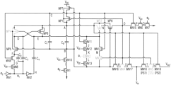
- FIG. 2 is a circuit diagram illustrating a bootstrap circuit according to an embodiment.
- the bootstrap circuit may receive an input signal through an input node and generate an output signal through the pre-charge operation and the sample operation.
- the input signal may have a voltage V IN higher than the power supply voltage V DD .
- a fifth NMOS transistor MN 5 which samples the input signal, may be referred to as a sampling switch SS.
- the bootstrap circuit may operate based on a first control signal ⁇ 1 and a second control signal ⁇ 2 .
- the first control signal ⁇ 1 may control a voltage applied to a gate of a second NMOS transistor MN 2 .
- the second control signal ⁇ 2 may control voltages applied to the gate of a first NMOS transistor MN 1 and the gate of a seventh NMOS transistor MN 7 , and one end of a first inverter INV 1 .
- the first to seventh transistors MN 1 to MN 7 operating based on the first control signal ⁇ 1 and the second control signal ⁇ 2 are turned on or off, whether the remaining transistors are turned on or off may also be determined.
- the first control signal ⁇ 1 and the second control signal ⁇ 2 may have different logic levels based on the pre-charge operation or sample operation of the bootstrap circuit.
- the bootstrap circuit may perform a pre-charge operation.
- the bootstrap switch may perform a sample operation.
- the bootstrap circuit may include a sampler 210 , a driver 220 , and a level shifter 230 .
- the sampler 210 may receive an input signal having a higher voltage than a power supply voltage V DD through an input terminal.
- the sampler 210 may generate an output signal having a higher voltage than the power supply voltage V DD by sampling the input signal.
- the sampler 210 may perform a pre-charge operation and a sample operation to generate an output signal.
- the sampler 210 may include a fifth NMOS transistor MN 5 , an eighteenth NMOS transistor MN 18 , and a nineteenth NMOS transistor MN 19 .
- the fifth NMOS transistor MN 5 which samples the input signal, may be referred to as the sampling switch SS.
- the eighteenth NMOS transistor MN 18 and the nineteenth NMOS transistor MN 19 maintain a turned-on state regardless of the pre-charge operation and the sample operation, thereby preventing a voltage higher than or equal to a voltage limit from being applied to the fifth NMOS transistor MN 5 .
- the eighteenth NMOS transistor MN 18 which is connected between the fifth NMOS transistor MN 5 and the input node, may be referred to as a first protection switch PS 1 .
- the nineteenth NMOS transistor MN 19 which is connected between the fifth NMOS transistor MN 5 and the output node, may be referred to as a second protection switch PS 2 .
- the eighteenth NMOS transistor MN 18 and the nineteenth NMOS transistor MN 19 which are connected to both ends of the fifth NMOS transistor MN 5 (that is the sampling switch SS) may be referred to as a double protection switch of the fifth NMOS transistor MN 5 .
- the eighteenth NMOS transistor MN 18 and the nineteenth NMOS transistor MN 19 may prevent a voltage higher than or equal to the voltage limit from being applied to the fifth NMOS transistor MN 5 .
- the driver 220 may include the first NMOS transistor MN 1 to a fourth NMOS transistor MN 4 , a sixth NMOS transistor MN 6 , the seventh NMOS transistor MN 7 , a tenth NMOS transistor MN 10 to a seventeenth NMOS transistor MN 17 , a first PMOS transistor MP 1 , a second PMOS transistor MP 2 , a seventh PMOS transistor MP 7 , an eighth PMOS transistor MP 8 , and a bootstrap capacitor C B .
- the seventh PMOS transistor MP 7 , the first PMOS transistor MP 1 , the bootstrap capacitor C B , the tenth NMOS transistor MN 10 , and the first NMOS transistor MN 1 may be connected in series.
- a drain of the seventh PMOS transistor MP 7 may be connected to the power supply terminal.
- the first PMOS transistor MP 1 may have a drain connected to a source of the seventh PMOS transistor MP 7 and a body connected to a body of the seventh PMOS transistor MP 7 .
- the bootstrap capacitor C B has one end connected to a source of the first PMOS transistor MP 1 and the other end connected to a drain of the tenth NMOS transistor MN 10 .
- a drain of the first NMOS transistor MN 1 may be connected to a source of the tenth NMOS transistor MN 10 and a source of the first NMOS transistor MN 1 may be connected to a ground terminal.
- the second PMOS transistor MP 2 , the eighth PMOS transistor MP 8 , the fifteenth NMOS transistor MN 15 , the sixth NMOS transistor MN 6 , and the seventh NMOS transistor MN 7 may be connected in series.
- a source and a body of the second PMOS transistor MP 2 may be connected to the source of the first PMOS transistor MP 1 .
- the eighth PMOS transistor MP 8 has a source connected to a drain of the second PMOS transistor MP 2 , a body connected to the body of the second PMOS transistor MP 2 , and a gate connected to the other end of the bootstrap capacitor C B , and a drain of the eighth PMOS transistor MP 8 may be connected to the gate of the fifth NMOS transistor MN 5 .
- a source of the fifteenth NMOS transistor MN 15 may be connected to a gate of the fifth NMOS transistor MN 5 .
- the source of the sixth NMOS transistor MN 6 may be connected to the drain of the fifteenth NMOS transistor MN 15 .
- the seventh NMOS transistor MN 7 may have a source connected to the drain of the sixth NMOS transistor MN 6 and a drain connected to the ground terminal.
- the sixteenth NMOS transistor MN 16 , the fourth NMOS transistor MN 4 , and the seventeenth NMOS transistor MN 17 may be connected in series.
- the source of the sixteenth NMOS transistor MN 16 may be connected to the other end of the bootstrap capacitor C B and the gate may be connected to the source of the first PMOS transistor MP 1 .
- the fourth NMOS transistor MN 4 may have a source connected to the drain of the sixteenth NMOS transistor MN 16 and a gate connected to a gate of the first PMOS transistor MP 1 .
- the seventeenth NMOS transistor MN 17 may have a source connected to a drain of the fourth NMOS transistor MN 4 , a gate connected to the source of the first PMOS transistor MP 1 , and a drain connected to the input node.
- the fourteenth NMOS transistor MN 14 and the third NMOS transistor MN 3 may be connected in series, and the eleventh NMOS transistor MN 11 , the twelfth NMOS transistor MN 12 , the second NMOS transistor MN 2 , and the thirteenth NMOS transistor MN 13 may be connected in series.
- the tenth NMOS transistor MN 10 to the seventeenth NMOS transistor MN 17 , the seventh PMOS transistor MP 7 , and the eighth PMOS transistor MP 8 maintain a turned-on state regardless of the pre-charge operation and the sample operation, so that it is possible to prevent a voltage higher than or equal to the voltage limit from being applied to the remaining transistors.
- the tenth NMOS transistor MN 10 may maintain a turned-on state regardless of the pre-charge operation and the sample operation, and may prevent a voltage higher than or equal to the voltage limit from being applied to the first NMOS transistor MN 1 by being connected in series with the first NMOS transistor MN 1 .
- the eleventh NMOS transistor MN 11 , the twelfth NMOS transistor MN 12 , and the thirteenth NMOS transistor MN 13 may prevent a voltage higher than or equal to the voltage limit from being applied to the second NMOS transistor MN 2
- the fourteenth NMOS transistor MN 14 may prevent a voltage higher than or equal to the voltage limit from being applied to the third NMOS transistor MN 3
- the fifteenth NMOS transistor MN 15 may prevent a voltage higher than or equal to the voltage limit from being applied to the sixth NMOS transistor MN 6
- the seventh PMOS transistor MP 7 may prevent a voltage higher than or equal to the voltage limit from being applied to the first PMOS transistor MP 1
- the eighth PMOS transistor MP 8 may prevent a voltage higher than or equal to the voltage limit from being applied to the second PMOS transistor MP 2 .
- the tenth NMOS transistor MN 10 to the seventeenth NMOS transistor MN 17 , the seventh PMOS transistor MP 7 , and the eighth PMOS transistor MP 8 may be referred to as stacked protection switches of transistors, to which a voltage higher than or equal to the voltage limit is prevented from being applied.
- the level shifter 230 may include the first inverter INV 1 , a second inverter INV 2 , a first capacitor C 1 to a fourth capacitor C 4 , an eighth NMOS transistor MN 8 , a ninth NMOS transistor MN 9 , and a fourth PMOS transistor MP 4 to a sixth PMOS transistor MP 6 .
- the level shifter 230 may control the voltage applied to a gate of the second PMOS transistor MP 2 based on the power supply voltage V DD and the input signal. Specifically, the level shifter 230 controls the power supply voltage V DD to be applied to the gate of the second PMOS transistor MP 2 during the pre-charge operation, so that the second PMOS transistor MP 2 may be turned off. Also, the level shifter 230 controls an input voltage to be applied to the gate of the second PMOS transistor MP 2 during the sample operation so that the second PMOS transistor MP 2 may be turned on.
- the fourth PMOS transistor MP 4 may have a drain and a body connected to the source of the first PMOS transistor MP 1 and a gate connected to the gate of the second PMOS transistor MP 2 .
- the fifth PMOS transistor MP 5 has a drain connected to the source of the fourth PMOS transistor MP 4 , a body connected to the body of the fourth PMOS transistor MP 4 , and a gate connected to the other end of the bootstrap capacitor C B .
- the sixth PMOS transistor MP 6 has a drain and a body connected to the drain of the fourth PMOS transistor MP 4 , a gate connected to the source of the fourth PMOS transistor MP 4 , and a source connected to a gate of the fourth PMOS transistor MP 4 .
- One end of the first capacitor C 1 may be connected to the source of the first PMOS transistor MP 1 and the other end may be connected to the gate of the fifth PMOS transistor MP 5 .
- the second capacitor C 2 has one end connected to a source of the fifth PMOS transistor MP 5 and the other end connected to the other end of the second inverter INV 2 .
- the third capacitor C 3 has one end connected to the gate of the fourth PMOS transistor MP 4 and the other end connected to one end of the second inverter INV 2 .
- the fourth capacitor C 4 may have one end connected to the source of the sixth PMOS transistor MP 6 and the other end connected to the other end of the second inverter INV 2 .
- the eighth NMOS transistor MN 8 may have a drain connected to the source of the ninth NMOS transistor MN 9 and a source connected to one end of the second inverter INV 2 .
- the ninth NMOS transistor MN 9 has a drain connected to the source of the fifth PMOS transistor MP 5 and a gate connected to the drain of the first PMOS transistor MP 1 .
- FIGS. 3 A and 3 B are diagrams illustrating an operation of a bootstrap circuit according to an embodiment
- FIG. 4 is a table showing voltages for each node of the bootstrap circuit according to an embodiment.
- FIG. 3 A may show a pre-charge operation of the bootstrap circuit when the voltage V IN of the input signal is greater than the power supply voltage V DD
- FIG. 3 B may show a sample operation of the bootstrap circuit when the voltage V IN of the input signal is greater than the power supply voltage V DD .
- the first control signal ⁇ 1 may have a low logic level and the second control signal ⁇ 2 may have a high logic level.
- a high logic level may correspond to a power supply voltage V DD
- a low logic level may correspond to a ground voltage.
- the second NMOS transistor MN 2 having a gate to which the first control signal ⁇ 1 is applied may be turned off.
- the first NMOS transistor MN 1 and the seventh NMOS transistor MN 7 having gates to which the second control signal ⁇ 2 is applied may be turned on.
- the bootstrap circuit may receive an input signal having a higher voltage than a power supply voltage V DD .
- the input signal may be a voltage higher than or equal to the voltage limit of transistors included in the bootstrap circuit.
- the power supply voltage V DD may be about 0.7 V
- the voltage limit of transistors may be about 0.95 V
- the voltage V IN of the input signal may be about 1.2 V.
- the sixth NMOS transistor MN 6 , the eighth NMOS transistor MN 8 , the tenth NMOS transistor MN 10 , the twelfth NMOS transistor MN 12 , and the thirteenth NMOS transistor MN 13 having gates to which the power supply voltage V DD is applied may be turned on.
- the third capacitor C 3 and the fourth capacitor C 4 may be in a discharged state. Therefore, a voltage of a node D may be the ground voltage that is a voltage of the first control signal ⁇ 1 . Accordingly, the sixth PMOS transistor MP 6 having a gate connected to the node D may be turned on. A voltage of a node H connected to the output terminal of the second inverter INV 2 may be the power supply voltage V DD , and a voltage of a node E may also be the power supply voltage V DD . Accordingly, the second PMOS transistor MP 2 and the fourth PMOS transistor MP 4 having gates connected to the node E may be turned off.
- a node B may be connected to the ground terminal to have a ground voltage, for example, about 0 V. Accordingly, the fifth PMOS transistor MP 5 , the seventh PMOS transistor MP 7 , and the eighth PMOS transistor MP 8 , the gates of which are connected to the node B, may be turned on.
- a node C may be connected to the power supply terminal, and a voltage of the node C may be the power supply voltage V DD .
- the ninth NMOS transistor MN 9 , the eleventh NMOS transistor MN 11 , the fourteenth NMOS transistor MN 14 , and the fifteenth NMOS transistor MN 15 having gates connected to the node C may be turned on.
- a node O may be connected to the ground terminal. Therefore, a voltage of the node O may be the ground voltage.
- the third NMOS transistor MN 3 to the fifth NMOS transistor MN 5 having gates connected to the node O may be turned off, and the first PMOS transistor MP 1 may be turned on.
- a node A may be connected to the power supply terminal. Therefore, a voltage of the node A may be the power supply voltage V DD .
- the sixteenth NMOS transistor MN 16 to the nineteenth NMOS transistor MN 19 having gates connected to the node A may be turned on.
- the seventh PMOS transistor MP 7 , the first PMOS transistor MP 1 , the tenth NMOS transistor MN 10 , and the first NMOS transistor MN 1 may be turned on, one end of the bootstrap capacitor C B may be connected to the power supply terminal, and the other end of the bootstrap capacitor C B may be connected to the ground terminal. Therefore, during the pre-charge operation, the bootstrap capacitor C B may be charged with the power supply voltage V DD .
- a voltage between a gate and a source of the fifth NMOS transistor MN 5 serving as a sampling switch and a voltage between a drain and a source of the fifth NMOS transistor MN 5 may be less than or equal to the power supply voltage V DD .
- a voltage between a gate and the source of the fourth NMOS transistor MN 4 and a voltage between the drain and the source of the fourth NMOS transistor MN 4 may be less than or equal to the power supply voltage V DD .
- the fifth NMOS transistor MN 5 serving as a sampling switch may not be destroyed.
- the eighteenth NMOS transistor MN 18 and the nineteenth NMOS transistor MN 19 which prevent the fifth NMOS transistor MN 5 from being destroyed, may be referred to as a double protection switch of the fifth NMOS transistor MN 5 .
- the sixteenth NMOS transistor MN 16 and the seventeenth NMOS transistor MN 17 which prevent the fourth NMOS transistor MN 4 from being destroyed, may be referred to as a double protection switch of the fourth NMOS transistor MN 4 .
- the first control signal ⁇ 1 may have a high logic level and the second control signal ⁇ 2 may have a low logic level.
- the second NMOS transistor MN 2 to which the first control signal ⁇ 1 is applied to the gate may be turned on.
- the first NMOS transistor MN 1 and the seventh NMOS transistor MN 7 to which the second control signal ⁇ 2 is applied to gates may be turned off.
- the bootstrap circuit may receive an input signal having a higher voltage than a power supply voltage V DD . Also, the voltage of the input signal may be higher than or equal to the voltage limit of transistors included in the bootstrap circuit.
- the sixth NMOS transistor MN 6 , the eighth NMOS transistor MN 8 , the tenth NMOS transistor MN 10 , the twelfth NMOS transistor MN 12 , and the thirteenth NMOS transistor MN 13 having gates to which the power supply voltage V DD is applied may be turned on.
- the bootstrap capacitor C B may be charged to the power supply voltage V DD during a pre-charge operation and then discharged during a sample operation. Therefore, the voltage of the node A may be higher than a voltage of the node B. Accordingly, the fifth PMOS transistor MP 5 , the seventh PMOS transistor MP 7 , and the eighth PMOS transistor MP 8 , the gates of which are connected to the node B and the bodies of which are connected to the node A, may be turned on. In addition, the sixteenth NMOS transistor MN 16 to the nineteenth NMOS transistor MN 19 having gates connected to the node A may be turned on.
- the voltage between the gate and the source of the sixteenth NMOS transistor MN 16 to the nineteenth NMOS transistor MN 19 may be maintained at the power supply voltage regardless of the voltage of the input signal due to the bootstrap capacitor C B .
- the linearity of the bootstrap capacitor C B may be secured.
- the voltage of the node C may be the power supply voltage V DD . Accordingly, the ninth NMOS transistor MN 9 , the eleventh NMOS transistor MN 11 , the fourteenth NMOS transistor MN 14 , and the fifteenth NMOS transistor MN 15 having gates connected to the node C may be turned on.
- the third capacitor C 3 may pull up the voltage of the node D during the sample operation. Accordingly, the sixth PMOS transistor MP 6 , the gate of which is connected to the node D, may be turned off.
- the fourth capacitor C 4 may pull down the voltage of the node E. Accordingly, the fourth PMOS transistor MP 4 , the gate of which is connected to the node E, may be turned on.
- the fourth capacitor C 4 may pull down the voltage of the node E, the voltage of the node E may be lower than the voltage of the node A. Accordingly, the second PMOS transistor MP 2 having a gate connected to the node E and a body connected to the node A may be turned on.
- the voltage of the node O may be the same as that of the node A.
- the voltage of the node O may be a higher voltage than the voltage of the node B by the voltage charged in the bootstrap capacitor C B .
- the voltages of the node A and the node O may be a voltage obtained by adding the power supply voltage V DD to the voltage V IN of the input signal.
- the first PMOS transistor MP 1 having a gate connected to the node O and a body connected to the node A may be turned off.
- the third NMOS transistor MN 3 to the fifth NMOS transistor MN 5 having gates connected to the node O may be turned on.
- the seventh PMOS transistor MP 7 may be turned on, the voltage between the gate and drain of the first PMOS transistor MP 1 may be less than or equal to the power supply voltage V DD .
- the fifteenth NMOS transistor MN 15 may be turned on, the voltage between the drain and source of the sixth NMOS transistor MN 6 may be less than the power supply voltage V DD .
- the tenth NMOS transistor MN 10 may be turned on, the voltage between the drain and source of the first NMOS transistor MN 1 may be less than or equal to the power supply voltage V DD .
- the bootstrap circuit according to the embodiment receives an input signal having a voltage higher than the power supply voltage V DD during the sample operation, the first PMOS transistor MP 1 , the sixth NMOS transistor MN 6 , and the first NMOS transistor MN 1 may not be destroyed.
- the seventh PMOS transistor MP 7 which prevents the first PMOS transistor MP 1 from being destroyed, may be referred to as a stacked protection switch of the first PMOS transistor MP 1 .
- the stacked protection switch may refer to a switch connected in series with a transistor to prevent a voltage higher than or equal to a voltage limit from being applied to the transistor. Therefore, the fifteenth NMOS transistor MN 15 and the tenth NMOS transistor MN 10 , which prevent the sixth NMOS transistor MN 6 and the first NMOS transistor MN 1 from being destroyed, may be referred to as a stacked protection switch of the sixth NMOS transistor MN 6 and a stacked protection switch of the first NMOS transistor MN 1 , respectively.
- the bootstrap circuit may include an eleventh NMOS transistor MN 11 to a fourteenth NMOS transistor MN 14 and an eighth PMOS transistor MP 8 .
- the eleventh NMOS transistor MN 11 to the thirteenth NMOS transistor MN 13 may be referred to as stacked protection switches of the second NMOS transistor MN 2 .
- the fourteenth NMOS transistor MN 14 may be referred to as a stacked protection switch of the third NMOS transistor MN 3 .
- the eighth PMOS transistor MP 8 may be referred to as a stacked protection switch of the second PMOS transistor MP 2 .
- the stack protection switch may prevent a voltage higher than the voltage limit from being applied to the first PMOS transistor MP 1 , the second PMOS transistor MP 2 , the first NMOS transistor MN 1 , the second NMOS transistor MN 2 , the third NMOS transistor MN 3 , and the sixth NMOS transistor MN 6 .
- transistors may not be destroyed.
- FIG. 5 is a diagram illustrating signals in a bootstrap circuit according to an embodiment.
- FIG. 5 the voltages of the node A and the node B are shown based on the first control signal ⁇ 1 , the second control signal ⁇ 2 , and the input signal.
- FIG. 5 may be described with reference to FIGS. 3 A and 3 B .
- the bootstrap circuit may perform a pre-charge operation.
- the voltage of the node A may be the power supply voltage V DD
- the voltage of the node B may be the ground voltage.
- the bootstrap circuit may perform a sample operation.
- the voltage of the node A may be the voltage obtained by adding the power supply voltage V DD to the voltage of the input signal
- the voltage of the node B may be the voltage of the input signal.
- FIG. 6 is a block diagram illustrating an Internet of things (IoT) device according to an embodiment.
- IoT Internet of things
- IoT may refer to a network between objects using wired/wireless communication.
- IoT devices may include devices that have accessible wired or wireless interfaces and transmit or receive data by communicating with at least one other device through the wired or wireless interface.
- the accessible interface may include a wired Local Area Network (LAN) interface, a Wireless Local Area Network (WLAN) interface, such as Wi-Fi, a Wireless Personal Area Network (WPAN) interface, such as Bluetooth, a Wireless Universal Serial Bus (USB) interface, a Zigbee interface, an NFC interface, a Radio-frequency identification (RFID) interface, a Power Line Communication (PLC) interface, or a modem communication interface capable of accessing a mobile cellular network, such as 3G, 4G, and LTE.
- the Bluetooth interface may support Bluetooth Low Energy (BLE).
- the IoT device 2000 may include a communication interface 2200 for communicating with the outside.
- the communication interface 2200 may be, for example, a LAN interface, a wireless local area communication interface, such as Bluetooth, Wi-Fi, Zigbee, a PLC interface, or a modem communication interface accessible to 3G, LTE, and the like.
- the communication interface 2200 may include a transceiver and/or receiver.
- the IoT device 2000 may transmit and/or receive information from an access point or gateway through the transceiver and/or receiver.
- the IoT device 2000 may transmit and/or receive control information or data of the IoT device 2000 by communicating with a user device or another IoT device.
- the receiver included in the communication interface 2200 may include a bootstrap circuit, and the bootstrap circuit may be implemented according to the above description with reference to FIGS. 1 to 5 .
- the bootstrap circuit may be implemented with the sampler 110 , driver 120 , and level shifter 130 of FIG. 1 .
- the bootstrap circuit may be implemented with the sampler 210 , the driver 220 , and the level shifter 230 of FIG. 2 .
- a receiver included in the communication interface 2200 may include a bootstrap circuit.
- the communication interface 2200 may further include a control circuit that controls the bootstrap circuit. The control circuit may generate a first control signal and a second control signal, and the bootstrap circuit may operate based on the first control signal and the second control signal, as described above with reference to FIGS. 1 to 5 .
- the IoT device 2000 may further include a processor or access point (AP) 2100 that performs calculations.
- the IoT device 2000 may further include a built-in battery for internal power supply or a power supply unit receiving external power.
- the IoT device 2000 may include a display 2400 for displaying an internal state or data.
- a user may control the IoT device 2000 through a user interface (UI) of the display 2400 of the IoT device 2000 .
- the IoT device 2000 may transmit an internal state and/or data to the outside through the transceiver and receive a control command and/or data from the outside through the receiver.
- UI user interface
- the memory 2300 may store control command codes for controlling the IoT device 2000 , control data, or user data.
- the memory 2300 may include at least one of volatile memory and non-volatile memory.
- the non-volatile memory may include at least one of various memories, such as read only memory (ROM), programmable ROM (PROM), electrically programmable ROM (EPROM), electrically erasable and programmable ROM (EEPROM), flash memory, phase-change RAM (PRAM), magnetic RAM (MRAM), Resistive RAM (ReRAM), and Ferroelectric RAM (FRAM).
- the volatile memory may include at least one of various memories, such as dynamic RAM (DRAM), static RAM (SRAM), and synchronous DRAM (SDRAM).
- the IoT device 2000 may further include a storage device.
- the storage device may be a nonvolatile medium, such as a hard disk (HDD), a solid state disk (SSD), an embedded multimedia card (eMMC), or a universal flash storage (UFS).
- the storage device may store user information provided through an input/output (I/O) 2500 and sensing information collected through a sensor 2600 .
- I/O input/output
Landscapes
- Engineering & Computer Science (AREA)
- Computer Hardware Design (AREA)
- Physics & Mathematics (AREA)
- Computing Systems (AREA)
- General Engineering & Computer Science (AREA)
- Mathematical Physics (AREA)
- Electronic Switches (AREA)
- Transmitters (AREA)
Abstract
Description
- This application is based on and claims priority under 35 U.S.C. § 119 to Korean Patent Application Nos. 10-2022-0144654, filed on Nov. 2, 2022, and 10-2023-0006317, filed on Jan. 16, 2023, in the Korean Intellectual Property Office, the disclosure of which is incorporated by reference herein in its entirety.
- The disclosure relates to a bootstrap circuit, and more particularly, to a bootstrap circuit for generating an output signal by sampling an input signal that is higher than a power supply voltage, and a communication device including the same.
- A sampling switch is used in various analog circuits such as analog multiplexers and sample-and-hold amplifiers (SHA). To process high-resolution analog signals, it is important to improve linearity of the sampling switch.
- The bootstrap circuit may be used to improve the linearity of the sampling switch. However, when the bootstrap circuit receives an analog input signal having a voltage level, which is higher than or equal to a limit of an input voltage of the sampling switch, there are some problems, for example, the sampling switch is destroyed or current leakage occurs.
- Provided are a bootstrap circuit capable of stable sampling of an input signal, which is higher than a power supply voltage, and a communication device including the same.
- According to an aspect of the disclosure, a bootstrap circuit for generating an output signal through a pre-charge operation and a sample operation, includes: a sampler including a sampling switch configured to sample an input signal, a first protection switch connected between an input node and the sampling switch, and a second protection switch connected between the sampling switch and an output node; and a driver configured to drive the sampler based on a power supply voltage and the input signal.
- According to another aspect of the disclosure, a bootstrap circuit includes: a sampler including a sampling switch configured to sample an input signal, a first protection switch connected between an input node and the sampling switch, and a second protection switch connected between the sampling switch and an output node; and a driver configured to drive the sampler by adjusting a voltage applied to the sampler based on a logic level of a control signal.
- According to another aspect of the disclosure, a communication device includes: a bootstrap circuit; and a control circuit configured to generate a control signal, wherein the bootstrap circuit includes: a sampler including a sampling switch configured to sample an input signal, a first protection switch connected between an input node and the sampling switch, and a second protection switch connected between the sampling switch and an output node; and a driver configured to drive the sampler based on the control signal.
- Embodiments will be more clearly understood from the following detailed description taken in conjunction with the accompanying drawings in which:
-
FIG. 1 is a block diagram illustrating a bootstrap circuit according to an embodiment; -
FIG. 2 is a circuit diagram illustrating a bootstrap circuit according to an embodiment; -
FIGS. 3A and 3B are diagrams illustrating the operation of a bootstrap circuit according to an embodiment; -
FIG. 4 is a table showing voltages per node of a bootstrap circuit according to an embodiment; -
FIG. 5 is a diagram illustrating signals in a bootstrap circuit according to an embodiment; and -
FIG. 6 is a block diagram illustrating an Internet of things (IoT) device according to an embodiment. - Hereinafter, one or more embodiments of the disclosure will be described with reference to the accompanying drawings.
-
FIG. 1 is a block diagram illustrating a bootstrap circuit according to an embodiment. - Bootstrap circuits may be included in or mounted on analog-to-digital converters (ADCs), digital signal processors (DSPs), central processor units (CPUs), graphics processing units (GPUs), micro-controllers, application specific integrated circuits (ASICs), field programmable gate arrays (FPGAs), programmable logic devices, and the like. Also, the bootstrap circuit may receive a power supply voltage from a charge pump. Referring to
FIG. 1 , the bootstrap circuit may include asampler 110, adriver 120, and alevel shifter 130. - In one embodiment, the
sampler 110 may receive an input signal IN having a voltage higher than the power supply voltage through an input terminal. Thesampler 110 may generate an output signal OUT having a higher voltage than the power supply voltage VDD by sampling the input signal IN. Thesampler 110 may perform a pre-charge operation and a sample operation to generate an output signal OUT. In one embodiment, when a first control signal has a low (L) logic level and a second control signal has a high (H) logic level, thesampler 110 may perform the pre-charge operation. On the other hand, when the first control signal has a high (H) logic level and the second control signal has a low (L) logic level, thesampler 110 may perform the sample operation. - The
sampler 110 may include asampling switch 111, afirst protection switch 112, and asecond protection switch 113. In the disclosure, a protection switch may refer to a switch arranged to prevent a voltage higher than or equal to a voltage limit from being applied to transistors included in a bootstrap circuit. For example, the protection switch may include an n-channel metal-oxide semiconductor (NMOS) transistor or a p-channel metal-oxide semiconductor (PMOS) transistor. - The
sampling switch 111 may sample the input signal IN. In the disclosure, thesampling switch 111 may refer to any switch that samples the input signal IN. For example, thesampling switch 111 may include an NMOS transistor. - In one embodiment, the
first protection switch 112 and thesecond protection switch 113 may refer to switches connected to thesampling switch 111 to prevent a voltage higher than or equal to a voltage limit from being applied to thesampling switch 111. - In the disclosure, a voltage limit may refer to a maximum voltage that a transistor may withstand before being destroyed. The voltage limit may be also referred to as a breakdown voltage in this disclosure.
- In one embodiment, the
first protection switch 112 may be connected between the input node and the sampling switch. Also, thesecond protection switch 113 may be connected between the sampling switch and the output node. In one embodiment, thefirst protection switch 112 and thesecond protection switch 113 may be turned on regardless of the pre-charge operation and the sample operation. - In one embodiment, the
driver 120 may drive thesampler 110 based on the power voltage VDD and the input signal IN. Specifically, thedriver 120 may control voltages applied to a gate of thesampling switch 111, a gate of thefirst protection switch 112, and a gate of thesecond protection switch 113 during the pre-charge operation and the sample operation. During the pre-charge operation, thedriver 120 may turn on thefirst protection switch 112 and thesecond protection switch 113. Also, during the pre-charge operation, thedriver 120 may turn off thesampling switch 111. During the sample operation, thedriver 120 may turn on thefirst protection switch 112, thesecond protection switch 113, and thesampling switch 111. Thedriver 120 may include a transistor for boosting a voltage of the input signal IN (e.g., a second PMOS transistor ofFIG. 2 ). - In one embodiment, the
level shifter 130 may control a voltage level of a gate of a transistor for boosting the voltage of the input signal IN. The operation of thelevel shifter 130 will be described later with reference toFIGS. 2 to 3B . - In some embodiments, the bootstrap circuit may operate based on a first control signal and a second control signal. The
driver 120 may receive the first control signal and the second control signal from a control circuit that controls the bootstrap circuit. For example, when the first control signal has a high (H) logic level, the bootstrap circuit may perform a sample operation. On the other hand, when the second control signal has a high logic level, the bootstrap circuit may perform a pre-charge operation. - In an embodiment of the disclosure, unlike in the related art, the bootstrap circuit may stably sample the input signal IN even if the input signal IN is higher than the power supply voltage VDD. In one embodiment, the bootstrap circuit may prevent the
sampling switch 111 and the transistors of the bootstrap circuit from being destroyed in the process of sampling the input signal IN higher than the power supply voltage VDD, andFIG. 2 is a circuit diagram illustrating a bootstrap circuit according to an embodiment. - Referring to
FIG. 2 , the bootstrap circuit may receive an input signal through an input node and generate an output signal through the pre-charge operation and the sample operation. The input signal may have a voltage VIN higher than the power supply voltage VDD. A fifth NMOS transistor MN5, which samples the input signal, may be referred to as a sampling switch SS. - Also, the bootstrap circuit may operate based on a first control signal Φ1 and a second control signal Φ2. Specifically, the first control signal Φ1 may control a voltage applied to a gate of a second NMOS transistor MN2. Also, the second control signal Φ2 may control voltages applied to the gate of a first NMOS transistor MN1 and the gate of a seventh NMOS transistor MN7, and one end of a first inverter INV1. As the first to seventh transistors MN1 to MN7 operating based on the first control signal Φ1 and the second control signal Φ2 are turned on or off, whether the remaining transistors are turned on or off may also be determined.
- The first control signal Φ1 and the second control signal Φ2 may have different logic levels based on the pre-charge operation or sample operation of the bootstrap circuit. When the first control signal Φ1 has a low (L) logic level and the second control signal Φ2 has a high (H) logic level, the bootstrap circuit may perform a pre-charge operation. On the other hand, when the first control signal Φ1 has a high (H) logic level and the second control signal Φ2 has a low (L) logic level, the bootstrap switch may perform a sample operation.
- Referring to
FIG. 2 , the bootstrap circuit may include asampler 210, adriver 220, and alevel shifter 230. - The
sampler 210 may receive an input signal having a higher voltage than a power supply voltage VDD through an input terminal. Thesampler 210 may generate an output signal having a higher voltage than the power supply voltage VDD by sampling the input signal. Thesampler 210 may perform a pre-charge operation and a sample operation to generate an output signal. - The
sampler 210 may include a fifth NMOS transistor MN5, an eighteenth NMOS transistor MN18, and a nineteenth NMOS transistor MN19. Here, the fifth NMOS transistor MN5, which samples the input signal, may be referred to as the sampling switch SS. The eighteenth NMOS transistor MN18 and the nineteenth NMOS transistor MN19 maintain a turned-on state regardless of the pre-charge operation and the sample operation, thereby preventing a voltage higher than or equal to a voltage limit from being applied to the fifth NMOS transistor MN5. - The eighteenth NMOS transistor MN18, which is connected between the fifth NMOS transistor MN5 and the input node, may be referred to as a first protection switch PS1. Also, the nineteenth NMOS transistor MN19, which is connected between the fifth NMOS transistor MN5 and the output node, may be referred to as a second protection switch PS2. The eighteenth NMOS transistor MN18 and the nineteenth NMOS transistor MN19, which are connected to both ends of the fifth NMOS transistor MN5 (that is the sampling switch SS) may be referred to as a double protection switch of the fifth NMOS transistor MN5. The eighteenth NMOS transistor MN18 and the nineteenth NMOS transistor MN19 may prevent a voltage higher than or equal to the voltage limit from being applied to the fifth NMOS transistor MN5.
- The
driver 220 may include the first NMOS transistor MN1 to a fourth NMOS transistor MN4, a sixth NMOS transistor MN6, the seventh NMOS transistor MN7, a tenth NMOS transistor MN10 to a seventeenth NMOS transistor MN17, a first PMOS transistor MP1, a second PMOS transistor MP2, a seventh PMOS transistor MP7, an eighth PMOS transistor MP8, and a bootstrap capacitor CB. - In one embodiment, as shown in
FIG. 2 , the seventh PMOS transistor MP7, the first PMOS transistor MP1, the bootstrap capacitor CB, the tenth NMOS transistor MN10, and the first NMOS transistor MN1 may be connected in series. - Specifically, a drain of the seventh PMOS transistor MP7 may be connected to the power supply terminal. The first PMOS transistor MP1 may have a drain connected to a source of the seventh PMOS transistor MP7 and a body connected to a body of the seventh PMOS transistor MP7. The bootstrap capacitor CB has one end connected to a source of the first PMOS transistor MP1 and the other end connected to a drain of the tenth NMOS transistor MN10. A drain of the first NMOS transistor MN1 may be connected to a source of the tenth NMOS transistor MN10 and a source of the first NMOS transistor MN1 may be connected to a ground terminal.
- The second PMOS transistor MP2, the eighth PMOS transistor MP8, the fifteenth NMOS transistor MN15, the sixth NMOS transistor MN6, and the seventh NMOS transistor MN7 may be connected in series.
- Specifically, a source and a body of the second PMOS transistor MP2 may be connected to the source of the first PMOS transistor MP1. The eighth PMOS transistor MP8 has a source connected to a drain of the second PMOS transistor MP2, a body connected to the body of the second PMOS transistor MP2, and a gate connected to the other end of the bootstrap capacitor CB, and a drain of the eighth PMOS transistor MP8 may be connected to the gate of the fifth NMOS transistor MN5.
- A source of the fifteenth NMOS transistor MN15 may be connected to a gate of the fifth NMOS transistor MN5. The source of the sixth NMOS transistor MN6 may be connected to the drain of the fifteenth NMOS transistor MN15. The seventh NMOS transistor MN7 may have a source connected to the drain of the sixth NMOS transistor MN6 and a drain connected to the ground terminal.
- The sixteenth NMOS transistor MN16, the fourth NMOS transistor MN4, and the seventeenth NMOS transistor MN17 may be connected in series.
- Specifically, the source of the sixteenth NMOS transistor MN16 may be connected to the other end of the bootstrap capacitor CB and the gate may be connected to the source of the first PMOS transistor MP1. The fourth NMOS transistor MN4 may have a source connected to the drain of the sixteenth NMOS transistor MN16 and a gate connected to a gate of the first PMOS transistor MP1.
- The seventeenth NMOS transistor MN17 may have a source connected to a drain of the fourth NMOS transistor MN4, a gate connected to the source of the first PMOS transistor MP1, and a drain connected to the input node.
- In addition, the fourteenth NMOS transistor MN14 and the third NMOS transistor MN3 may be connected in series, and the eleventh NMOS transistor MN11, the twelfth NMOS transistor MN12, the second NMOS transistor MN2, and the thirteenth NMOS transistor MN13 may be connected in series.
- The tenth NMOS transistor MN10 to the seventeenth NMOS transistor MN17, the seventh PMOS transistor MP7, and the eighth PMOS transistor MP8 maintain a turned-on state regardless of the pre-charge operation and the sample operation, so that it is possible to prevent a voltage higher than or equal to the voltage limit from being applied to the remaining transistors.
- Specifically, the tenth NMOS transistor MN10 may maintain a turned-on state regardless of the pre-charge operation and the sample operation, and may prevent a voltage higher than or equal to the voltage limit from being applied to the first NMOS transistor MN1 by being connected in series with the first NMOS transistor MN1.
- Similarly, the eleventh NMOS transistor MN11, the twelfth NMOS transistor MN12, and the thirteenth NMOS transistor MN13 may prevent a voltage higher than or equal to the voltage limit from being applied to the second NMOS transistor MN2, and the fourteenth NMOS transistor MN14 may prevent a voltage higher than or equal to the voltage limit from being applied to the third NMOS transistor MN3. In addition, the fifteenth NMOS transistor MN15 may prevent a voltage higher than or equal to the voltage limit from being applied to the sixth NMOS transistor MN6, and the seventh PMOS transistor MP7 may prevent a voltage higher than or equal to the voltage limit from being applied to the first PMOS transistor MP1. The eighth PMOS transistor MP8 may prevent a voltage higher than or equal to the voltage limit from being applied to the second PMOS transistor MP2.
- The tenth NMOS transistor MN10 to the seventeenth NMOS transistor MN17, the seventh PMOS transistor MP7, and the eighth PMOS transistor MP8 may be referred to as stacked protection switches of transistors, to which a voltage higher than or equal to the voltage limit is prevented from being applied.
- The
level shifter 230 may include the first inverter INV1, a second inverter INV2, a first capacitor C1 to a fourth capacitor C4, an eighth NMOS transistor MN8, a ninth NMOS transistor MN9, and a fourth PMOS transistor MP4 to a sixth PMOS transistor MP6. - The
level shifter 230 may control the voltage applied to a gate of the second PMOS transistor MP2 based on the power supply voltage VDD and the input signal. Specifically, thelevel shifter 230 controls the power supply voltage VDD to be applied to the gate of the second PMOS transistor MP2 during the pre-charge operation, so that the second PMOS transistor MP2 may be turned off. Also, thelevel shifter 230 controls an input voltage to be applied to the gate of the second PMOS transistor MP2 during the sample operation so that the second PMOS transistor MP2 may be turned on. - The fourth PMOS transistor MP4 may have a drain and a body connected to the source of the first PMOS transistor MP1 and a gate connected to the gate of the second PMOS transistor MP2.
- The fifth PMOS transistor MP5 has a drain connected to the source of the fourth PMOS transistor MP4, a body connected to the body of the fourth PMOS transistor MP4, and a gate connected to the other end of the bootstrap capacitor CB.
- The sixth PMOS transistor MP6 has a drain and a body connected to the drain of the fourth PMOS transistor MP4, a gate connected to the source of the fourth PMOS transistor MP4, and a source connected to a gate of the fourth PMOS transistor MP4.
- One end of the first capacitor C1 may be connected to the source of the first PMOS transistor MP1 and the other end may be connected to the gate of the fifth PMOS transistor MP5.
- The second capacitor C2 has one end connected to a source of the fifth PMOS transistor MP5 and the other end connected to the other end of the second inverter INV2.
- The third capacitor C3 has one end connected to the gate of the fourth PMOS transistor MP4 and the other end connected to one end of the second inverter INV2. The fourth capacitor C4 may have one end connected to the source of the sixth PMOS transistor MP6 and the other end connected to the other end of the second inverter INV2.
- The eighth NMOS transistor MN8 may have a drain connected to the source of the ninth NMOS transistor MN9 and a source connected to one end of the second inverter INV2.
- The ninth NMOS transistor MN9 has a drain connected to the source of the fifth PMOS transistor MP5 and a gate connected to the drain of the first PMOS transistor MP1.
-
FIGS. 3A and 3B are diagrams illustrating an operation of a bootstrap circuit according to an embodiment, andFIG. 4 is a table showing voltages for each node of the bootstrap circuit according to an embodiment.FIG. 3A may show a pre-charge operation of the bootstrap circuit when the voltage VIN of the input signal is greater than the power supply voltage VDD, andFIG. 3B may show a sample operation of the bootstrap circuit when the voltage VIN of the input signal is greater than the power supply voltage VDD. - Referring to
FIGS. 3A and 4 together, during the pre-charge operation, the first control signal Φ1 may have a low logic level and the second control signal Φ2 may have a high logic level. In the disclosure, a high logic level may correspond to a power supply voltage VDD, and a low logic level may correspond to a ground voltage. The second NMOS transistor MN2 having a gate to which the first control signal Φ1 is applied may be turned off. Also, the first NMOS transistor MN1 and the seventh NMOS transistor MN7 having gates to which the second control signal Φ2 is applied may be turned on. - The bootstrap circuit may receive an input signal having a higher voltage than a power supply voltage VDD. Also, the input signal may be a voltage higher than or equal to the voltage limit of transistors included in the bootstrap circuit. For example, the power supply voltage VDD may be about 0.7 V, the voltage limit of transistors may be about 0.95 V, and the voltage VIN of the input signal may be about 1.2 V.
- The sixth NMOS transistor MN6, the eighth NMOS transistor MN8, the tenth NMOS transistor MN10, the twelfth NMOS transistor MN12, and the thirteenth NMOS transistor MN13 having gates to which the power supply voltage VDD is applied may be turned on.
- The third capacitor C3 and the fourth capacitor C4 may be in a discharged state. Therefore, a voltage of a node D may be the ground voltage that is a voltage of the first control signal Φ1. Accordingly, the sixth PMOS transistor MP6 having a gate connected to the node D may be turned on. A voltage of a node H connected to the output terminal of the second inverter INV2 may be the power supply voltage VDD, and a voltage of a node E may also be the power supply voltage VDD. Accordingly, the second PMOS transistor MP2 and the fourth PMOS transistor MP4 having gates connected to the node E may be turned off.
- Since the tenth NMOS transistor MN10 and the first NMOS transistor MN1 may be turned on, a node B may be connected to the ground terminal to have a ground voltage, for example, about 0 V. Accordingly, the fifth PMOS transistor MP5, the seventh PMOS transistor MP7, and the eighth PMOS transistor MP8, the gates of which are connected to the node B, may be turned on.
- Since the seventh PMOS transistor MP7 may be turned on, a node C may be connected to the power supply terminal, and a voltage of the node C may be the power supply voltage VDD. Thus, the ninth NMOS transistor MN9, the eleventh NMOS transistor MN11, the fourteenth NMOS transistor MN14, and the fifteenth NMOS transistor MN15 having gates connected to the node C may be turned on.
- Since the fifteenth NMOS transistor MN15, the sixth NMOS transistor MN6, and the seventh NMOS transistor MN7 may be turned on, a node O may be connected to the ground terminal. Therefore, a voltage of the node O may be the ground voltage. The third NMOS transistor MN3 to the fifth NMOS transistor MN5 having gates connected to the node O may be turned off, and the first PMOS transistor MP1 may be turned on.
- Since the first PMOS transistor MP1 and the seventh PMOS transistor MP7 may be turned on, a node A may be connected to the power supply terminal. Therefore, a voltage of the node A may be the power supply voltage VDD. The sixteenth NMOS transistor MN16 to the nineteenth NMOS transistor MN19 having gates connected to the node A may be turned on.
- Since the seventh PMOS transistor MP7, the first PMOS transistor MP1, the tenth NMOS transistor MN10, and the first NMOS transistor MN1 may be turned on, one end of the bootstrap capacitor CB may be connected to the power supply terminal, and the other end of the bootstrap capacitor CB may be connected to the ground terminal. Therefore, during the pre-charge operation, the bootstrap capacitor CB may be charged with the power supply voltage VDD.
- Since the eighteenth NMOS transistor MN18 and the nineteenth NMOS transistor MN19 may be turned on, a voltage between a gate and a source of the fifth NMOS transistor MN5 serving as a sampling switch and a voltage between a drain and a source of the fifth NMOS transistor MN5 may be less than or equal to the power supply voltage VDD.
- Similarly, since the sixteenth NMOS transistor MN16 and the seventeenth NMOS transistor MN17 may be turned on, a voltage between a gate and the source of the fourth NMOS transistor MN4 and a voltage between the drain and the source of the fourth NMOS transistor MN4 may be less than or equal to the power supply voltage VDD.
- Therefore, even if the bootstrap circuit according to the embodiment receives an input signal having a voltage higher than the power supply voltage VDD during a pre-charge operation, the fifth NMOS transistor MN5 serving as a sampling switch may not be destroyed. Here, the eighteenth NMOS transistor MN18 and the nineteenth NMOS transistor MN19, which prevent the fifth NMOS transistor MN5 from being destroyed, may be referred to as a double protection switch of the fifth NMOS transistor MN5. Also, the sixteenth NMOS transistor MN16 and the seventeenth NMOS transistor MN17, which prevent the fourth NMOS transistor MN4 from being destroyed, may be referred to as a double protection switch of the fourth NMOS transistor MN4.
- Referring to
FIGS. 3B and 4 together, during a sample operation, the first control signal Φ1 may have a high logic level and the second control signal Φ2 may have a low logic level. The second NMOS transistor MN2 to which the first control signal Φ1 is applied to the gate may be turned on. Also, the first NMOS transistor MN1 and the seventh NMOS transistor MN7 to which the second control signal Φ2 is applied to gates may be turned off. - The bootstrap circuit may receive an input signal having a higher voltage than a power supply voltage VDD. Also, the voltage of the input signal may be higher than or equal to the voltage limit of transistors included in the bootstrap circuit.
- The sixth NMOS transistor MN6, the eighth NMOS transistor MN8, the tenth NMOS transistor MN10, the twelfth NMOS transistor MN12, and the thirteenth NMOS transistor MN13 having gates to which the power supply voltage VDD is applied may be turned on.
- The bootstrap capacitor CB may be charged to the power supply voltage VDD during a pre-charge operation and then discharged during a sample operation. Therefore, the voltage of the node A may be higher than a voltage of the node B. Accordingly, the fifth PMOS transistor MP5, the seventh PMOS transistor MP7, and the eighth PMOS transistor MP8, the gates of which are connected to the node B and the bodies of which are connected to the node A, may be turned on. In addition, the sixteenth NMOS transistor MN16 to the nineteenth NMOS transistor MN19 having gates connected to the node A may be turned on. In other words, the voltage between the gate and the source of the sixteenth NMOS transistor MN16 to the nineteenth NMOS transistor MN19 may be maintained at the power supply voltage regardless of the voltage of the input signal due to the bootstrap capacitor CB. Through this, the linearity of the bootstrap capacitor CB may be secured.
- Since the seventh PMOS transistor MP7 may be turned on, the voltage of the node C may be the power supply voltage VDD. Accordingly, the ninth NMOS transistor MN9, the eleventh NMOS transistor MN11, the fourteenth NMOS transistor MN14, and the fifteenth NMOS transistor MN15 having gates connected to the node C may be turned on.
- The third capacitor C3 may pull up the voltage of the node D during the sample operation. Accordingly, the sixth PMOS transistor MP6, the gate of which is connected to the node D, may be turned off. The fourth capacitor C4 may pull down the voltage of the node E. Accordingly, the fourth PMOS transistor MP4, the gate of which is connected to the node E, may be turned on.
- Since the fourth capacitor C4 may pull down the voltage of the node E, the voltage of the node E may be lower than the voltage of the node A. Accordingly, the second PMOS transistor MP2 having a gate connected to the node E and a body connected to the node A may be turned on.
- Since the second PMOS transistor MP2 and the eighth PMOS transistor MP8 may be turned on, the voltage of the node O may be the same as that of the node A. In other words, the voltage of the node O may be a higher voltage than the voltage of the node B by the voltage charged in the bootstrap capacitor CB. Specifically, the voltages of the node A and the node O may be a voltage obtained by adding the power supply voltage VDD to the voltage VIN of the input signal. Accordingly, the first PMOS transistor MP1 having a gate connected to the node O and a body connected to the node A may be turned off. Also, the third NMOS transistor MN3 to the fifth NMOS transistor MN5 having gates connected to the node O may be turned on.
- Since the seventh PMOS transistor MP7 may be turned on, the voltage between the gate and drain of the first PMOS transistor MP1 may be less than or equal to the power supply voltage VDD. Similarly, since the fifteenth NMOS transistor MN15 may be turned on, the voltage between the drain and source of the sixth NMOS transistor MN6 may be less than the power supply voltage VDD. Also, since the tenth NMOS transistor MN10 may be turned on, the voltage between the drain and source of the first NMOS transistor MN1 may be less than or equal to the power supply voltage VDD.
- Therefore, even if the bootstrap circuit according to the embodiment receives an input signal having a voltage higher than the power supply voltage VDD during the sample operation, the first PMOS transistor MP1, the sixth NMOS transistor MN6, and the first NMOS transistor MN1 may not be destroyed.
- Here, the seventh PMOS transistor MP7, which prevents the first PMOS transistor MP1 from being destroyed, may be referred to as a stacked protection switch of the first PMOS transistor MP1. Here, the stacked protection switch may refer to a switch connected in series with a transistor to prevent a voltage higher than or equal to a voltage limit from being applied to the transistor. Therefore, the fifteenth NMOS transistor MN15 and the tenth NMOS transistor MN10, which prevent the sixth NMOS transistor MN6 and the first NMOS transistor MN1 from being destroyed, may be referred to as a stacked protection switch of the sixth NMOS transistor MN6 and a stacked protection switch of the first NMOS transistor MN1, respectively.
- When switching from pre-charge operation to sample operation or from sample operation to pre-charge operation, a voltage greater than or equal to the voltage limit may be momentarily applied to the second NMOS transistor MN2, the third NMOS transistor MN3, and the second PMOS transistor MP2. To prevent this, the bootstrap circuit may include an eleventh NMOS transistor MN11 to a fourteenth NMOS transistor MN14 and an eighth PMOS transistor MP8.
- The eleventh NMOS transistor MN11 to the thirteenth NMOS transistor MN13 may be referred to as stacked protection switches of the second NMOS transistor MN2. The fourteenth NMOS transistor MN14 may be referred to as a stacked protection switch of the third NMOS transistor MN3. The eighth PMOS transistor MP8 may be referred to as a stacked protection switch of the second PMOS transistor MP2.
- When an input signal higher than the power supply voltage VDD is applied, the stack protection switch may prevent a voltage higher than the voltage limit from being applied to the first PMOS transistor MP1, the second PMOS transistor MP2, the first NMOS transistor MN1, the second NMOS transistor MN2, the third NMOS transistor MN3, and the sixth NMOS transistor MN6.
- Thus, in a bootstrap circuit according to an embodiment, during the sample operation, since a voltage higher than or equal to the voltage limit may not be applied to the first NMOS transistor MN1 to the seventh NMOS transistor MN7, the first PMOS transistor MP1, and the second PMOS transistor MP2, transistors may not be destroyed.
-
FIG. 5 is a diagram illustrating signals in a bootstrap circuit according to an embodiment. - Referring to
FIG. 5 , the voltages of the node A and the node B are shown based on the first control signal Φ1, the second control signal Φ2, and the input signal.FIG. 5 may be described with reference toFIGS. 3A and 3B . - When the first control signal Φ1 has a low logic level and the second control signal Φ2 has a high logic level, the bootstrap circuit may perform a pre-charge operation. At this time, the voltage of the node A may be the power supply voltage VDD, and the voltage of the node B may be the ground voltage.
- When the first control signal Φ1 is at a high logic level and the second control signal Φ2 is at a low logic level, the bootstrap circuit may perform a sample operation. At this time, the voltage of the node A may be the voltage obtained by adding the power supply voltage VDD to the voltage of the input signal, and the voltage of the node B may be the voltage of the input signal.
-
FIG. 6 is a block diagram illustrating an Internet of things (IoT) device according to an embodiment. - Referring to
FIG. 6 , a bootstrap circuit according to embodiments of the disclosure may be included in anIoT device 2000. IoT may refer to a network between objects using wired/wireless communication. IoT devices may include devices that have accessible wired or wireless interfaces and transmit or receive data by communicating with at least one other device through the wired or wireless interface. The accessible interface may include a wired Local Area Network (LAN) interface, a Wireless Local Area Network (WLAN) interface, such as Wi-Fi, a Wireless Personal Area Network (WPAN) interface, such as Bluetooth, a Wireless Universal Serial Bus (USB) interface, a Zigbee interface, an NFC interface, a Radio-frequency identification (RFID) interface, a Power Line Communication (PLC) interface, or a modem communication interface capable of accessing a mobile cellular network, such as 3G, 4G, and LTE. The Bluetooth interface may support Bluetooth Low Energy (BLE). - Specifically, the
IoT device 2000 may include acommunication interface 2200 for communicating with the outside. Thecommunication interface 2200 may be, for example, a LAN interface, a wireless local area communication interface, such as Bluetooth, Wi-Fi, Zigbee, a PLC interface, or a modem communication interface accessible to 3G, LTE, and the like. Thecommunication interface 2200 may include a transceiver and/or receiver. TheIoT device 2000 may transmit and/or receive information from an access point or gateway through the transceiver and/or receiver. In addition, theIoT device 2000 may transmit and/or receive control information or data of theIoT device 2000 by communicating with a user device or another IoT device. - In this embodiment, the receiver included in the
communication interface 2200 may include a bootstrap circuit, and the bootstrap circuit may be implemented according to the above description with reference toFIGS. 1 to 5 . For example, the bootstrap circuit may be implemented with thesampler 110,driver 120, andlevel shifter 130 ofFIG. 1 . In addition, the bootstrap circuit may be implemented with thesampler 210, thedriver 220, and thelevel shifter 230 ofFIG. 2 . Specifically, a receiver included in thecommunication interface 2200 may include a bootstrap circuit. Also, thecommunication interface 2200 may further include a control circuit that controls the bootstrap circuit. The control circuit may generate a first control signal and a second control signal, and the bootstrap circuit may operate based on the first control signal and the second control signal, as described above with reference toFIGS. 1 to 5 . - The
IoT device 2000 may further include a processor or access point (AP) 2100 that performs calculations. TheIoT device 2000 may further include a built-in battery for internal power supply or a power supply unit receiving external power. In addition, theIoT device 2000 may include adisplay 2400 for displaying an internal state or data. A user may control theIoT device 2000 through a user interface (UI) of thedisplay 2400 of theIoT device 2000. TheIoT device 2000 may transmit an internal state and/or data to the outside through the transceiver and receive a control command and/or data from the outside through the receiver. - The
memory 2300 may store control command codes for controlling theIoT device 2000, control data, or user data. Thememory 2300 may include at least one of volatile memory and non-volatile memory. The non-volatile memory may include at least one of various memories, such as read only memory (ROM), programmable ROM (PROM), electrically programmable ROM (EPROM), electrically erasable and programmable ROM (EEPROM), flash memory, phase-change RAM (PRAM), magnetic RAM (MRAM), Resistive RAM (ReRAM), and Ferroelectric RAM (FRAM). The volatile memory may include at least one of various memories, such as dynamic RAM (DRAM), static RAM (SRAM), and synchronous DRAM (SDRAM). - The
IoT device 2000 may further include a storage device. The storage device may be a nonvolatile medium, such as a hard disk (HDD), a solid state disk (SSD), an embedded multimedia card (eMMC), or a universal flash storage (UFS). The storage device may store user information provided through an input/output (I/O) 2500 and sensing information collected through asensor 2600. - While the disclosure has been particularly shown and described with reference to embodiments thereof, it will be understood that various changes in form and details may be made therein without departing from the spirit and scope of the following claims.
Claims (20)
Applications Claiming Priority (4)
| Application Number | Priority Date | Filing Date | Title |
|---|---|---|---|
| KR20220144654 | 2022-11-02 | ||
| KR10-2022-0144654 | 2022-11-02 | ||
| KR1020230006317A KR20240062871A (en) | 2022-11-02 | 2023-01-16 | Bootstrap circuit and communication device including the same |
| KR10-2023-0006317 | 2023-01-16 |
Publications (1)
| Publication Number | Publication Date |
|---|---|
| US20240146292A1 true US20240146292A1 (en) | 2024-05-02 |
Family
ID=88647493
Family Applications (1)
| Application Number | Title | Priority Date | Filing Date |
|---|---|---|---|
| US18/386,122 Pending US20240146292A1 (en) | 2022-11-02 | 2023-11-01 | Bootstrap circuit and communication device including the same |
Country Status (3)
| Country | Link |
|---|---|
| US (1) | US20240146292A1 (en) |
| EP (1) | EP4365903B1 (en) |
| TW (1) | TW202429809A (en) |
Cited By (3)
| Publication number | Priority date | Publication date | Assignee | Title |
|---|---|---|---|---|
| US20250015791A1 (en) * | 2023-07-05 | 2025-01-09 | Stmicroelectronics International N.V. | Half-bridge circuit for two-wire buses |
| CN121461996A (en) * | 2026-01-05 | 2026-02-03 | 成都纳川微电子科技有限公司 | Bootstrap sampling switch circuit with precharge and analog-to-digital converter |
| US12620983B2 (en) * | 2023-07-05 | 2026-05-05 | Stmicroelectronics International N.V. | Half-bridge circuit for two-wire buses |
Family Cites Families (2)
| Publication number | Priority date | Publication date | Assignee | Title |
|---|---|---|---|---|
| US9325312B1 (en) * | 2014-12-11 | 2016-04-26 | Freescale Semiconductor, Inc. | Input control circuit for analog device |
| US9484905B1 (en) * | 2016-01-22 | 2016-11-01 | Freescale Semiconductor, Inc. | Voltage sampling switch and method therefor |
-
2023
- 2023-11-01 EP EP23207302.3A patent/EP4365903B1/en active Active
- 2023-11-01 US US18/386,122 patent/US20240146292A1/en active Pending
- 2023-11-01 TW TW112142095A patent/TW202429809A/en unknown
Cited By (3)
| Publication number | Priority date | Publication date | Assignee | Title |
|---|---|---|---|---|
| US20250015791A1 (en) * | 2023-07-05 | 2025-01-09 | Stmicroelectronics International N.V. | Half-bridge circuit for two-wire buses |
| US12620983B2 (en) * | 2023-07-05 | 2026-05-05 | Stmicroelectronics International N.V. | Half-bridge circuit for two-wire buses |
| CN121461996A (en) * | 2026-01-05 | 2026-02-03 | 成都纳川微电子科技有限公司 | Bootstrap sampling switch circuit with precharge and analog-to-digital converter |
Also Published As
| Publication number | Publication date |
|---|---|
| EP4365903B1 (en) | 2026-01-28 |
| EP4365903A1 (en) | 2024-05-08 |
| TW202429809A (en) | 2024-07-16 |
Similar Documents
| Publication | Publication Date | Title |
|---|---|---|
| US9893738B2 (en) | Analog-to-digital converter and communication device including the same | |
| KR101875577B1 (en) | Apparatus for low power write and read operations for resistive memory | |
| US10547322B2 (en) | Analog-digital converter having multiple feedback, and communication device including the analog-digital converter | |
| US9330747B2 (en) | Non-volatile latch using spin-transfer torque memory device | |
| CN106981312B (en) | Electronic device and driving method thereof | |
| US20250182805A1 (en) | Read operations based on a dynamic reference | |
| US11495321B2 (en) | Method for setting a reference voltage for read operations | |
| US20240146292A1 (en) | Bootstrap circuit and communication device including the same | |
| US20080158986A1 (en) | Flash memory and associated methods | |
| US20220020415A1 (en) | Arbitrated sense amplifier | |
| US7869252B2 (en) | Ferroelectric memory device, method for driving ferroelectric memory device, and electronic equipment | |
| US20200144910A1 (en) | Electronic circuit including charge pump for converting voltage | |
| US20230084481A1 (en) | Read algorithm for memory device | |
| KR101604933B1 (en) | Tile-level snapback detection through coupling capacitor in a cross point array | |
| US7151682B2 (en) | Method and apparatus to read information from a content addressable memory (CAM) cell | |
| US8634258B2 (en) | Reduced signal interface memory device, system, and method | |
| US6552942B2 (en) | Data line precharging circuit of a semiconductor memory device | |
| CN117997318A (en) | Bootstrap circuit and communication device including the same | |
| CN102298967A (en) | Row decoding circuit of double-dissociation grid flash memory array and driving method thereof | |
| KR20240062871A (en) | Bootstrap circuit and communication device including the same | |
| CN106575525A (en) | Semiconductor storage device | |
| US12437787B2 (en) | Threshold compensated detector for memory sense | |
| US12567845B2 (en) | Amplifier and electronic system including the same | |
| KR100221801B1 (en) | Semiconductor memory device | |
| EP4521405B1 (en) | A non-volatile memory, related integrated circuit, electronic system and method |
Legal Events
| Date | Code | Title | Description |
|---|---|---|---|
| AS | Assignment |
Owner name: SAMSUNG ELECTRONICS CO., LTD., KOREA, REPUBLIC OF Free format text: ASSIGNMENT OF ASSIGNORS INTEREST;ASSIGNORS:LEE, SANGHEON;LEE, JUNGHO;CHO, YOUNGJAE;AND OTHERS;REEL/FRAME:065424/0243 Effective date: 20230620 |
|
| STPP | Information on status: patent application and granting procedure in general |
Free format text: DOCKETED NEW CASE - READY FOR EXAMINATION |
|
| STPP | Information on status: patent application and granting procedure in general |
Free format text: NON FINAL ACTION MAILED |
|
| STPP | Information on status: patent application and granting procedure in general |
Free format text: FINAL REJECTION MAILED |
|
| STPP | Information on status: patent application and granting procedure in general |
Free format text: RESPONSE AFTER FINAL ACTION FORWARDED TO EXAMINER |
|
| STPP | Information on status: patent application and granting procedure in general |
Free format text: ADVISORY ACTION COUNTED, NOT YET MAILED |
|
| STPP | Information on status: patent application and granting procedure in general |
Free format text: ADVISORY ACTION MAILED |
|
| STPP | Information on status: patent application and granting procedure in general |
Free format text: DOCKETED NEW CASE - READY FOR EXAMINATION |
|
| STPP | Information on status: patent application and granting procedure in general |
Free format text: NON FINAL ACTION COUNTED, NOT YET MAILED |
|
| STPP | Information on status: patent application and granting procedure in general |
Free format text: NON FINAL ACTION MAILED |
|
| STPP | Information on status: patent application and granting procedure in general |
Free format text: NON FINAL ACTION MAILED |
|
| STPP | Information on status: patent application and granting procedure in general |
Free format text: RESPONSE TO NON-FINAL OFFICE ACTION ENTERED AND FORWARDED TO EXAMINER |
|
| STPP | Information on status: patent application and granting procedure in general |
Free format text: ALLOWED -- NOTICE OF ALLOWANCE NOT YET MAILED |
|
| STPP | Information on status: patent application and granting procedure in general |
Free format text: NOTICE OF ALLOWANCE MAILED -- APPLICATION RECEIVED IN OFFICE OF PUBLICATIONS |