US20220108994A1 - Manufacturing method of semiconductor memory device - Google Patents
Manufacturing method of semiconductor memory device Download PDFInfo
- Publication number
- US20220108994A1 US20220108994A1 US17/223,448 US202117223448A US2022108994A1 US 20220108994 A1 US20220108994 A1 US 20220108994A1 US 202117223448 A US202117223448 A US 202117223448A US 2022108994 A1 US2022108994 A1 US 2022108994A1
- Authority
- US
- United States
- Prior art keywords
- layer
- insulating layer
- forming
- bit line
- stack structure
- Prior art date
- Legal status (The legal status is an assumption and is not a legal conclusion. Google has not performed a legal analysis and makes no representation as to the accuracy of the status listed.)
- Granted
Links
Images


Classifications
-
- H01L27/1157—
-
- H—ELECTRICITY
- H10—SEMICONDUCTOR DEVICES; ELECTRIC SOLID-STATE DEVICES NOT OTHERWISE PROVIDED FOR
- H10B—ELECTRONIC MEMORY DEVICES
- H10B43/00—EEPROM devices comprising charge-trapping gate insulators
- H10B43/20—EEPROM devices comprising charge-trapping gate insulators characterised by three-dimensional [3D] arrangements, e.g. with cells on different height levels
- H10B43/23—EEPROM devices comprising charge-trapping gate insulators characterised by three-dimensional [3D] arrangements, e.g. with cells on different height levels with source and drain on different levels, e.g. with sloping channels
- H10B43/27—EEPROM devices comprising charge-trapping gate insulators characterised by three-dimensional [3D] arrangements, e.g. with cells on different height levels with source and drain on different levels, e.g. with sloping channels the channels comprising vertical portions, e.g. U-shaped channels
-
- H01L21/32133—
-
- H01L21/32139—
-
- H01L23/5225—
-
- H01L23/5226—
-
- H01L23/535—
-
- H01L27/11524—
-
- H01L27/11529—
-
- H01L27/11556—
-
- H01L27/11573—
-
- H01L27/11582—
-
- H—ELECTRICITY
- H10—SEMICONDUCTOR DEVICES; ELECTRIC SOLID-STATE DEVICES NOT OTHERWISE PROVIDED FOR
- H10B—ELECTRONIC MEMORY DEVICES
- H10B41/00—Electrically erasable-and-programmable ROM [EEPROM] devices comprising floating gates
- H10B41/20—Electrically erasable-and-programmable ROM [EEPROM] devices comprising floating gates characterised by three-dimensional [3D] arrangements, e.g. with cells on different height levels
- H10B41/23—Electrically erasable-and-programmable ROM [EEPROM] devices comprising floating gates characterised by three-dimensional [3D] arrangements, e.g. with cells on different height levels with source and drain on different levels, e.g. with sloping channels
- H10B41/27—Electrically erasable-and-programmable ROM [EEPROM] devices comprising floating gates characterised by three-dimensional [3D] arrangements, e.g. with cells on different height levels with source and drain on different levels, e.g. with sloping channels the channels comprising vertical portions, e.g. U-shaped channels
-
- H—ELECTRICITY
- H10—SEMICONDUCTOR DEVICES; ELECTRIC SOLID-STATE DEVICES NOT OTHERWISE PROVIDED FOR
- H10B—ELECTRONIC MEMORY DEVICES
- H10B41/00—Electrically erasable-and-programmable ROM [EEPROM] devices comprising floating gates
- H10B41/30—Electrically erasable-and-programmable ROM [EEPROM] devices comprising floating gates characterised by the memory core region
- H10B41/35—Electrically erasable-and-programmable ROM [EEPROM] devices comprising floating gates characterised by the memory core region with a cell select transistor, e.g. NAND
-
- H—ELECTRICITY
- H10—SEMICONDUCTOR DEVICES; ELECTRIC SOLID-STATE DEVICES NOT OTHERWISE PROVIDED FOR
- H10B—ELECTRONIC MEMORY DEVICES
- H10B41/00—Electrically erasable-and-programmable ROM [EEPROM] devices comprising floating gates
- H10B41/40—Electrically erasable-and-programmable ROM [EEPROM] devices comprising floating gates characterised by the peripheral circuit region
- H10B41/41—Electrically erasable-and-programmable ROM [EEPROM] devices comprising floating gates characterised by the peripheral circuit region of a memory region comprising a cell select transistor, e.g. NAND
-
- H—ELECTRICITY
- H10—SEMICONDUCTOR DEVICES; ELECTRIC SOLID-STATE DEVICES NOT OTHERWISE PROVIDED FOR
- H10B—ELECTRONIC MEMORY DEVICES
- H10B43/00—EEPROM devices comprising charge-trapping gate insulators
- H10B43/10—EEPROM devices comprising charge-trapping gate insulators characterised by the top-view layout
-
- H—ELECTRICITY
- H10—SEMICONDUCTOR DEVICES; ELECTRIC SOLID-STATE DEVICES NOT OTHERWISE PROVIDED FOR
- H10B—ELECTRONIC MEMORY DEVICES
- H10B43/00—EEPROM devices comprising charge-trapping gate insulators
- H10B43/30—EEPROM devices comprising charge-trapping gate insulators characterised by the memory core region
- H10B43/35—EEPROM devices comprising charge-trapping gate insulators characterised by the memory core region with cell select transistors, e.g. NAND
-
- H—ELECTRICITY
- H10—SEMICONDUCTOR DEVICES; ELECTRIC SOLID-STATE DEVICES NOT OTHERWISE PROVIDED FOR
- H10B—ELECTRONIC MEMORY DEVICES
- H10B43/00—EEPROM devices comprising charge-trapping gate insulators
- H10B43/40—EEPROM devices comprising charge-trapping gate insulators characterised by the peripheral circuit region
-
- H—ELECTRICITY
- H10—SEMICONDUCTOR DEVICES; ELECTRIC SOLID-STATE DEVICES NOT OTHERWISE PROVIDED FOR
- H10P—GENERIC PROCESSES OR APPARATUS FOR THE MANUFACTURE OR TREATMENT OF DEVICES COVERED BY CLASS H10
- H10P50/00—Etching of wafers, substrates or parts of devices
- H10P50/20—Dry etching; Plasma etching; Reactive-ion etching
- H10P50/26—Dry etching; Plasma etching; Reactive-ion etching of conductive or resistive materials
- H10P50/264—Dry etching; Plasma etching; Reactive-ion etching of conductive or resistive materials by chemical means
-
- H—ELECTRICITY
- H10—SEMICONDUCTOR DEVICES; ELECTRIC SOLID-STATE DEVICES NOT OTHERWISE PROVIDED FOR
- H10P—GENERIC PROCESSES OR APPARATUS FOR THE MANUFACTURE OR TREATMENT OF DEVICES COVERED BY CLASS H10
- H10P50/00—Etching of wafers, substrates or parts of devices
- H10P50/71—Etching of wafers, substrates or parts of devices using masks for conductive or resistive materials
-
- H—ELECTRICITY
- H10—SEMICONDUCTOR DEVICES; ELECTRIC SOLID-STATE DEVICES NOT OTHERWISE PROVIDED FOR
- H10W—GENERIC PACKAGES, INTERCONNECTIONS, CONNECTORS OR OTHER CONSTRUCTIONAL DETAILS OF DEVICES COVERED BY CLASS H10
- H10W20/00—Interconnections in chips, wafers or substrates
- H10W20/20—Interconnections within wafers or substrates, e.g. through-silicon vias [TSV]
-
- H—ELECTRICITY
- H10—SEMICONDUCTOR DEVICES; ELECTRIC SOLID-STATE DEVICES NOT OTHERWISE PROVIDED FOR
- H10W—GENERIC PACKAGES, INTERCONNECTIONS, CONNECTORS OR OTHER CONSTRUCTIONAL DETAILS OF DEVICES COVERED BY CLASS H10
- H10W20/00—Interconnections in chips, wafers or substrates
- H10W20/40—Interconnections external to wafers or substrates, e.g. back-end-of-line [BEOL] metallisations or vias connecting to gate electrodes
- H10W20/41—Interconnections external to wafers or substrates, e.g. back-end-of-line [BEOL] metallisations or vias connecting to gate electrodes characterised by their conductive parts
- H10W20/42—Vias, e.g. via plugs
-
- H—ELECTRICITY
- H10—SEMICONDUCTOR DEVICES; ELECTRIC SOLID-STATE DEVICES NOT OTHERWISE PROVIDED FOR
- H10W—GENERIC PACKAGES, INTERCONNECTIONS, CONNECTORS OR OTHER CONSTRUCTIONAL DETAILS OF DEVICES COVERED BY CLASS H10
- H10W20/00—Interconnections in chips, wafers or substrates
- H10W20/40—Interconnections external to wafers or substrates, e.g. back-end-of-line [BEOL] metallisations or vias connecting to gate electrodes
- H10W20/41—Interconnections external to wafers or substrates, e.g. back-end-of-line [BEOL] metallisations or vias connecting to gate electrodes characterised by their conductive parts
- H10W20/423—Shielding layers
Definitions
- the present disclosure may generally relate to a manufacturing method of a semiconductor memory device, and more particularly, to a manufacturing method of a three-dimensional semiconductor memory device.
- a semiconductor memory device includes a plurality of memory cells capable of storing data.
- the memory cells may be three-dimensionally arranged to implement a three-dimensional semiconductor memory device.
- the memory cells may constitute a plurality of memory cell strings.
- the memory cell strings may be connected to word lines and select lines.
- a method of manufacturing a semiconductor memory device including: forming a preliminary memory cell array on a support structure, the preliminary memory cell array with a stack structure and cell pillars; removing the support structure to expose a portion of each of the cell pillars; forming a protective layer that covers the exposed portion of each of the cell pillars; forming a mask pattern that exposes an opening defined between inclined surfaces of the protective layer, wherein the inclined surfaces are disposed between the cell pillars; and etching at least one conductive layer among the conductive layers that is adjacent to the opening, thereby isolating the at least one conductive layer into select lines.
- FIG. 1 is a circuit diagram illustrating a memory block of a semiconductor memory device in accordance with an embodiment of the present disclosure.
- FIGS. 2A and 2B are perspective views illustrating semiconductor memory devices in accordance with embodiments of the present disclosure.
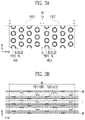
- FIG. 3A illustrates a layout of a gate stack structure and channel structures of a semiconductor memory device in accordance with an embodiment of the present disclosure
- FIG. 3B illustrates a layout of bit lines.
- FIG. 4 is a flowchart schematically illustrating a manufacturing method of a semiconductor memory device in accordance with an embodiment of the present disclosure.
- FIGS. 5A to 5L are sectional views illustrating a manufacturing method of a semiconductor memory device in accordance with an embodiment of the present disclosure.
- FIGS. 6A to 6C are sectional views illustrating an embodiment of a process of forming an impurity injection region shown in FIG. 5F .
- FIGS. 7A to 7H are sectional views illustrating a manufacturing method of a semiconductor memory device in accordance with an embodiment of the present disclosure.
- FIG. 8 is a block diagram illustrating a configuration of a memory system in accordance with an embodiment of the present disclosure.
- FIG. 9 is a block diagram illustrating a configuration of a computing system in accordance with an embodiment of the present disclosure.
- first and ‘second’ are used to distinguish one component from another component.
- the terms may be used to describe various components, but the components are not limited by the terms.
- Same reference numerals refer to same elements throughout the specification. Thus, even though a reference numeral is not mentioned or described with reference to a drawing, the reference numeral may be mentioned or described with reference to another drawing. In addition, even though a reference numeral is not shown in a drawing, it may be mentioned or described with reference to another drawing.
- Embodiments may provide a manufacturing method of a semiconductor memory device, which can improve operational characteristics of the semiconductor memory device.
- FIG. 1 is a circuit diagram illustrating a memory block BLK of a semiconductor memory device in accordance with an embodiment of the present disclosure.
- the semiconductor memory device may include the memory block BLK.
- the memory block BLK may include a plurality of memory cell strings MS 1 and MS 2 that are connected to a source layer SL and a plurality of bit lines BL.
- Each of the memory cell strings MS 1 and MS 2 may include a plurality of memory cells MC that are connected in series, at least one source select transistor SST, and at least one drain select transistor DST.
- each of the memory cell strings MS 1 and MS 2 may include one source select transistor SST that is connected between the plurality of memory cells MC and the source layer SL.
- each of the memory cell strings MS 1 and MS 2 may include two or more source select transistors SST that are connected in series between the plurality of memory cells MC and the source layer SL.
- each of the memory cell strings MS 1 and MS 2 may include one drain select transistor DST that is connected between the plurality of memory cells MC and a bit line BL.
- each of the memory cell strings MS 1 and MS 2 may include two or more drain select transistors DST that are connected in series between the plurality of memory cells MC and the bit line BL.
- the plurality of memory cells MC may be connected to the source layer SL via the source select transistor SST.
- the plurality of memory cells MC may be connected to the bit line BL via the drain select transistor DST.
- Gates of source select transistors SST that are disposed at the same level may be connected to source select lines SSL 1 and SSL 2 isolated from each other.
- Gates of drain select transistors DST that are disposed at the same level may be connected to drain select lines DSL 1 and DSL 2 that are isolated from each other.
- Gates of the memory cells MC may be respectively connected to a plurality of word lines WL.
- the word lines WL may be disposed at different levels, and gates of memory cells MC that are disposed at the same level may be connected to a single word line WL.
- the memory block BLK with a first source select line SSL 1 and a second source select line SSL 2 that are isolated from each other at the same level and a first drain select line DSL 1 and a second drain select line DSL 2 that are isolated from each other at the same level is exemplified in the drawing.
- the present disclosure is not limited thereto.
- the memory block BLK may include three or more source select lines that are isolated from one another at the same level.
- the memory block BLK may include three or more drain select lines that are isolated from one another at the same level.
- the plurality of memory cell strings MS 1 and MS 2 may be connected to each of the word lines WL.
- the plurality of memory cell strings MS 1 and MS 2 may include a first group and a second group, which can be individually selected by the first source select line SSL 1 and the second source select line SSL 2 .
- the first group may include first memory cell strings MS 1
- the second group may include second memory cell strings MS 2 .
- Memory cells MC of the first memory cell strings MS 1 may be respectively connected to the bit lines BL via drain select transistors DST that are connected to first drain select lines DSL 1 .
- Memory cells MC of the second memory cell strings MS 2 may be respectively connected to the bit lines BL via drain select transistor DST that is connected to second drain select lines DSL 2 .
- One of the first memory cell strings MS 1 and one of the second memory cell strings MS 2 may be connected to a single bit line BL.
- the memory cells MC of the first memory cell strings MS 1 may be connected to the source layer SL based on a gate signal applied to the first source select line SSL.
- the memory cells MC of the second memory cell strings MS 2 may be connected to the source layer SL based on a gate signal to the second source select line SSL 2 . Accordingly, the plurality of memory cell strings MS 1 and MS 2 may be isolated into groups that can be individually and simultaneously selected for each of the source select lines SSL 1 and SSL 2 in a read operation or a verify operation.
- one of the first source select line SSL 1 and a second source select line SSL 2 may be selected so that one group of the first group of the first memory cell strings MS 1 and the second group of the second memory cell strings MS 2 may be connected to the source layer SL. Accordingly, in the embodiment of the present disclosure, channel resistance may be reduced as compared with a case in which the first memory cell strings MS 1 and the second memory cell strings MS 2 are simultaneously connected to the source layer SL in the read operation or the verify operation. Thus, in the embodiment of the present disclosure, read disturb may be reduced.
- FIGS. 2A and 2B are perspective views illustrating semiconductor memory devices 1 A and 1 B in accordance with embodiments of the present disclosure.
- FIGS. 2A and 2B illustrate a portion of a configuration of each of the semiconductor memory devices 1 A and 1 B to help with the understanding of the structure of each of the semiconductor memory devices 1 A and 1 B.
- each of the semiconductor memory devices 1 A and 1 B may include a peripheral circuit structure 10 A or 10 B, a memory cell array 5 A to 5 B, a source layer 20 A or 20 B, and a plurality of bit lines 80 A or 80 B.
- the peripheral circuit structure 10 A or 10 B nay include a substrate extending in a first direction D 1 and a second direction D 2 .
- the peripheral circuit structure 10 A or 10 B may include a peripheral circuit that controls an operation of the memory cell array 5 A or 5 B. After the memory cell array 5 A or 5 B is manufactured, a structure with the memory cell array 5 A or 5 B may be bonded to the peripheral circuit structure 10 A or 10 B. Thus, the peripheral circuit structure 10 A or 10 B may be prevented from being damaged by heat that is generated while the memory cell array 5 A or 5 B is being manufactured. Accordingly, the operational characteristic degradation of the peripheral circuit structure 10 A or 10 B may be reduced.
- the memory cell array 5 A or may overlap with the peripheral circuit structure 10 A or 10 B.
- the memory cell array 5 A or 5 B may be disposed between the source layer 20 A or 20 B and the plurality of bit lines 80 A or 80 B.
- the arrangement of the memory cell array 5 A or 5 B, the source layer 20 A or 20 B, and the plurality of bit lines 80 A or 80 B in the third direction D 3 may vary.
- the memory cell array 5 A may overlap with the peripheral circuit structure 10 A, the source layer 20 A being interposed therebetween.
- the plurality of bit lines 80 A may overlap with the peripheral circuit structure 10 A, the source layer 20 A, and the memory cell array 5 A, the source layer 20 A and the memory cell array 5 A being interposed between the plurality of bit lines 80 A and the peripheral circuit structure 10 A.
- the memory cell array 5 A may include channel structures 60 A 1 and 60 A 2 and a gate stack structure 90 A that surrounds the channel structures 60 A 1 and 60 A 2 .
- the gate stack structure 90 A may include source select lines 31 A 1 , 31 A 2 , 32 A 1 , and 32 A 2 , word lines 40 A, and drain select lines 51 A 1 , 51 A 2 , 52 A 1 , and 52 A 2 .
- the source select lines 31 A 1 , 31 A 2 , 32 A 1 , and 32 A 2 , the word lines 40 A, and the drain select lines 51 A 1 , 51 A 2 , 52 A 1 , and 52 A 2 may be disposed to be spaced apart from each other.
- Conductive materials that constitute the source select lines 31 A 1 , 31 A 2 , 32 A 1 , and 32 A 2 , the word lines 40 A, and the drain select lines 51 A 1 , 51 A 2 , 52 A 1 , and 52 A 2 may vary.
- the source select lines 31 A 1 , 31 A 2 , 32 A 1 , and 32 A 2 and the drain select lines 51 A 1 , 51 A 2 , 52 A 1 , and 52 A 2 may be formed of the same conductive material as the word lines 40 A.
- the present disclosure is not limited thereto.
- the source select lines 31 A 1 , 31 A 2 , 32 A 1 , and 32 A 2 or the drain select lines 51 A 1 , 51 A 2 , 52 A 1 , and 52 A 2 may be formed of a conductive material that is different from that constituting the word lines 40 A.
- the source select lines 31 A 1 , 31 A 2 , 32 A 1 , and 32 A 2 may be disposed between the source layer 20 A and the plurality of bit lines 80 A.
- the source select lines 31 A 1 , 31 A 2 , 32 A 1 , and 32 A 2 may include at least one first source select line and at least one second source select line.
- the source select lines 31 A 1 , 31 A 2 , 32 A 1 , and 32 A 2 may include two first source select lines 31 A 1 and 32 A 1 and two second source select lines 31 A 2 and 32 A 2 .
- the first source select lines 31 A 1 and 32 A 1 may include a first source select line 31 A 1 of a first level and a first source select line 32 A 1 of a second level, which are spaced apart from each other in the third direction D 3 .
- the second source select lines 31 A 2 and 32 A 2 may include a second source select line 31 A 2 of the first level and a second source select line 32 A 2 of the second level, which are spaced apart from each other in the third direction D 3 .
- the first source select line 31 A 1 of the first level and the second source select line 31 A 2 of the first level may be spaced apart from each other in the first direction D 1 .
- the first source select line 32 A 1 of the second level and the second source select line 32 A 2 of the second level may be spaced apart from each other in the first direction D 1 .
- the drain select lines 51 A 1 , 51 A 2 , 52 A 1 , and 52 A 2 may be disposed between the source select lines 31 A 1 , 31 A 2 , 32 A 1 , and 32 A 2 and the plurality of bit lines 80 A.
- the drain select lines 51 A 1 , 51 A 2 , 52 A 1 , and 52 A 2 may include at least one first drain select line and at least one second drain select line.
- the drain select lines 51 A 1 , 51 A 2 , 52 A 1 , and 52 A 2 may include two first drain select lines 51 A 1 and 52 A 1 and two second drain select lines 51 A 2 and 52 A 2 .
- the first drain select lines 51 A 1 and 52 A 1 may include a first drain select line 51 A 1 of a third level and a first drain select line 52 A 1 of a fourth level, which are spaced apart from each other in the third direction D 3 .
- the second drain select lines 51 A 2 and 52 A 2 may include a second drain select line 51 A 2 of the third level and a second drain select line 52 A 2 of the fourth level, which are spaced apart from each other in the third direction D 3 .
- the first drain select line 51 A 1 of the third level and the second drain select line 51 A 2 of the third level may be spaced apart from each other in the first direction D 1 .
- the first drain select line 52 A 1 of the fourth level and the second drain select line 52 A 2 of the fourth level may be spaced apart from each other in the first direction D 1 .
- Each of the word lines 40 A may be disposed between the first source select lines 31 A 1 and 32 A 1 and the first drain select lines 51 A 1 and 52 A 1 , and may extend between the second source select lines 31 A 2 and 32 A 2 and the second drain select lines 51 A 2 and 52 A 2 .
- the word lines 40 A may be stacked to be spaced apart from each other in the third direction D 3 .
- the channel structures 60 A 1 and 60 A 2 may include a channel layer that is used as a channel region of the memory cell strings MS 1 and MS 2 , shown in FIG. 1 .
- the channel structures 60 A 1 and 60 A 2 may be in contact with the source layer 20 A.
- the channel structures 60 A 1 and 60 A 2 may penetrate the gate stack structure 90 A and may extend toward the bit lines 80 A.
- the channel structures 60 A 1 and 60 A 2 may be connected to the bit lines 80 A via bit line contacts 70 A 1 and 70 A 2 .
- the channel structures 60 A 1 and 60 A 2 may include a first channel structure 60 A 1 that is controlled by the first source select lines 31 A 1 and 32 A 1 and a second channel structure 60 A 2 that is controlled by the second source select lines 31 A 2 and 32 A 2 .
- the first channel structure 60 A 1 may penetrate the first drain select lines 51 A and 52 A 1 , the word lines 40 A, and the first source select lines 31 A 1 and 32 A 1 , and may be in contact with the source layer 20 A.
- the second channel structure 60 A 2 may penetrate the second drain select lines 51 A 1 and 52 A 2 , the word lines 40 A, and the second source select lines 31 A 2 and 32 A 2 , and may be in contact with the source layer 20 A.
- Each of the word lines 40 A may extend to surround the first channel structure 60 A 1 and the second channel structure 60 A 2 . Accordingly, the first channel structure 60 A 1 and the second channel structure 60 A 2 may be simultaneously controlled by one word line 40 A.
- the bit line contacts 70 A 1 and 70 A 2 may include a first bit line contact 70 A 1 that is in contact with the first channel structure 60 A 1 and a second bit line contact 70 A 2 that is in contact with the second channel structure 60 A 2 .
- One bit line 80 A may be simultaneously connected to one first channel structure 60 A 1 and one second channel structure 60 A 2 via a pair of first and second bit line contacts 70 A 1 and 70 A 2 .
- the memory cell array 5 B may overlap with the peripheral circuit structure 10 B, the plurality of bit lines 80 B being interposed therebetween.
- the source layer 20 B may overlap with the peripheral circuit structure 10 B, the plurality of bit lines 80 B, and the memory cell array 5 B, the plurality of bit lines 80 B and the memory cell array 5 B being interposed between the source layer 20 B and the peripheral circuit structure 10 B.
- the memory cell array 56 may include channel structures 60 B 1 and 60 B 2 and a gate stack structure 90 B that surrounds the channel structures 60 B 1 and 60 B 2 .
- the gate stack structure 90 B may include source select lines 30 B 1 and 30 B 2 , word lines 40 B, and drain select lines 51 B 1 , 51 B 2 , 52 B 1 , and 52 B 2 .
- Conductive materials that constitute the source select lines 30 B 1 and 30 B 2 , the word lines 40 B, and the drain select lines 51 B 1 , 51 B 2 , 52 B 1 , and 52 B 2 may vary.
- detailed descriptions of components that overlap with those that are shown in FIG. 2A will be omitted.
- the drain select lines 51 B 1 , 51 B 2 , 52 B 1 , and 52 B 2 may be disposed between the plurality of bit lines 80 B and the source layer 20 B.
- the drain select lines 51 B 1 , 51 B 2 , 52 B 1 , and 52 B 2 may include two first drain select lines 51 B 1 and 52 B 1 and two second drain select lines 51 B 2 and 52 B 2 .
- the first drain select lines 51 B 1 and 52 B 1 may include a first drain select line 51 B 1 of a first level and a first drain select line 52 B 1 of a second level, which are spaced apart from each other in the third direction D 3 .
- the second drain select lines 51 B 2 and 52 B 2 may include a second drain select line 51 B 2 of the first level and a second drain select line 52 B 2 of the second level, which are spaced apart from each other in the third direction D 3 .
- the first drain select line 51 B 1 of the first level and the second drain select line 51 B 2 of the first level may be spaced apart from each other in the first direction D 1 .
- the first drain select line 52 B 1 of the second level and the second drain select line 52 B 2 of the second level may be spaced apart from each other in the first direction D 1 .
- the source select lines 30 B 1 and 30 B 2 may be disposed between the drain select lines 51 B 1 , 51 B 2 , 52 B 1 , and 52 B 2 and the source layer 20 B.
- a conductive layer of a third level may be isolated into line patterns so that a first source select line 30 B 1 and a second source select line 30 B 2 may be defined.
- the channel structures 60 B 1 and 60 B 2 may include a first channel structure 60 B 1 and a second channel structure 60 B 2 , which can be simultaneously controlled by one bit line 80 B.
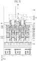
- FIG. 3A illustrates a layout of a gate stack structure 90 and channel structures 60 [ 1 ] and 60 [ 2 ] of a semiconductor memory device in accordance with an embodiment of the present disclosure
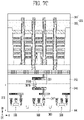
- FIG. 3B illustrates a layout of bit lines 80 .
- the layout of the gate stack structure 90 and the channel structures 60 [ 1 ] and 60 [ 2 ], which are shown in FIG. 3A , and the layout of the bit lines 80 A, shown in FIG. 3B may be applied to the semiconductor memory device 1 A, shown in FIG. 2A , or the semiconductor memory device 1 B, shown in FIG. 2B .
- the gate stack structure 90 may surround a first channel structure 60 [ 1 ] and a second channel structure 60 [ 2 ].
- a memory layer 61 may be disposed between the gate stack structure 90 and each of the first channel structure 60 [ 1 ] and the second channel structure 60 [ 2 ].
- the memory layer 61 may include a tunnel insulating layer 67 that surrounds each of the first channel structure 60 [ 1 ] and the second channel structure 60 [ 2 ], a data storage layer 65 that surrounds the tunnel insulating layer 67 , and a blocking insulating layer 63 that surrounds the data storage layer 65 .
- the data storage layer 65 may be formed as a material layer that is capable of storing data.
- the data storage layer 65 may be formed as a material layer that is capable of storing data, changed through Fowler-Nordheim tunneling.
- the material layer may include a nitride layer in which charges can be trapped.
- the blocking insulating layer 63 may include an oxide layer that is capable of blocking charges.
- the tunnel insulating layer 67 may be formed as a silicon oxide layer through which charges can tunnel.
- the first channel structure 60 [ 1 ] and the memory layer 61 that surrounds the first channel structure 60 [ 1 ] may constitute a first cell pillar 69 [ 1 ].
- the second channel structure 60 [ 2 ] and the memory layer 61 that surrounds the second channel structure 60 [ 2 ] may constitute a second cell pillar 69 [ 2 ].
- a plurality of first cell pillars 69 [ 1 ] and a plurality of second cell pillars 69 [ 2 ] may penetrate the gate stack structure 90 .
- the plurality of first cell pillars 69 [ 1 ] and the plurality of second cell pillars 69 [ 2 ] may be variously arranged on a plane that extends in the first direction D 1 and the second direction D 2 .
- the first cell pillars 69 [ 1 ] and the second cell pillars 69 [ 2 ] may constitute a zigzag arrangement to improve the arrangement density of memory cell strings.
- a first select line 35 [ 1 ] and a second select line 35 [ 2 ] of the gate stack structure 90 may be arranged to be spaced apart from each other in the first direction D 1 .
- Each of the first select line 35 [ 1 ] and the second select line 35 [ 2 ] may extend in the second direction D 2 .
- a layout of the first select line 35 [ 1 ] and the second select line 35 [ 2 ] may be applied to the first source select line 31 A 1 of the first level and the second source select line 31 A 2 of the first level, which are shown in FIG. 2A , and applied to the first source select line 32 A 1 of the second level and the second source select line 32 A 2 of the second level, which are shown in FIG. 2A .
- the layout of the first select line 35 [ 1 ] and the second select line 35 [ 2 ] may be applied to the first source select line 30 B 1 and the second source select line 30 B 2 , which are shown in FIG. 2B .
- the layout of the first select line 35 [ 1 ] and the second select line 35 [ 2 ] may be applied to the first drain select line 51 A 1 of the third level and the second drain select line 51 A 2 of the third level, which are shown in FIG. 2A , and applied to the first drain select line 52 A 1 of the fourth level and the second drain select line 52 A 2 of the fourth level, which are shown in FIG. 2A .
- the layout of the first select line 35 [ 1 ] and the second select line 35 [ 2 ] may be applied to the first drain select line 51 B 1 of the first level and the second drain select line 51 B 2 of the first level, which are shown in FIG. 2B , and applied to the first drain select line 52 B 1 of the second level and the second drain select line 52 B 2 of the second level, which are shown in FIG. 2B .
- the first select line 35 [ 1 ] and the second select line 35 [ 2 ] may be spaced apart from each other by a slit 37 .
- the slit 37 may overlap with a word line 40 of the gate stack structure 90 .
- the first cell pillars 69 [ 1 ] may include a slit-side first cell pillar that is adjacent to the slit 37
- the second cell pillars 69 [ 2 ] may include a slit-side second cell pillar that is adjacent to the slit 37 .
- a process of forming the slit 37 may be controlled such that the sidewall of the slit-side first cell pillar and the sidewall of the slit-side second cell pillar are not exposed.
- the process of forming the slit 37 may be performed through an embodiment, shown in FIGS. 5G to 5I , or may be performed through an embodiment, shown in FIG. 7E .
- the first select line 35 [ 1 ] may remain to surround the sidewall of the slit-side first cell pillar
- the second select line 35 [ 2 ] may remain to surround the sidewall of the slit-side second cell pillar.
- select transistors with a gate all around (GAA) structure may be defined at an intersection portion of the slit-side first cell pillar and the first select line 35 [ 1 ] and an intersection portion of the slit-side second cell pillar and the second select line 35 [ 2 ].
- GAA gate all around
- the bit lines 80 may overlap with the gate stack structure 90 .
- Each of the bit lines 80 may be simultaneously connected to one first channel structure 60 [ 1 ] and one second channel structure 60 [ 2 ] via a pair of first and second bit line contacts 70 [ 1 ] and 70 [ 2 ].
- a layout of the first and second bit line contacts 70 [ 1 ] and 70 [ 2 ] may vary based on the bit lines 80 and the first cannel structure 60 [ 1 ] and the second channel structure 60 [ 2 ].
- FIG. 4 is a flowchart schematically illustrating a manufacturing method of a semiconductor memory device in accordance with an embodiment of the present disclosure.
- a preliminary memory cell array may be provided through a process ST 1 of forming the preliminary memory cell array.
- the preliminary memory cell array may include conductive layers and interlayer insulating layers, which are alternately stacked on a support structure. At least one conductive layer among the conductive layers that is adjacent to the support structure may constitute select lines.
- a peripheral circuit may be bonded through a bonding process ST 3 .
- the bonding process ST 3 may be performed in a state in which the at least one conductive layer that is adjacent to the support structure is not isolated into the select lines.
- a process ST 5 of opening cell pillars may be performed.
- the cell pillars may be opened by removing the support structure.
- the opened cell pillars may provide an uneven structure.
- a process ST 7 of forming a protective layer may be performed.
- the protective layer may be deposited to cover the uneven structure that is provided by the cell pillars.
- the protective layer may be deposited under a condition in which step coverage is poor.
- the protective layer may be deposited through Physical Vapor Deposition (PVD) or Chemical Vapor Deposition (CVD), which has step coverage that is poorer than that of Atomic Layer Deposition (ALD).
- the protective layer may include a material with etch selectivity with respect to the interlayer insulating layers and the conductive layers of the preliminary memory cell array.
- the protective layer may include an amorphous carbon layer (ACL).
- the ACL may be deposited through Plasma Enhanced-Chemical Vapor Deposition (PE-CVD).
- the protective layer that is deposited under the condition in which the step coverage is poor may be formed relatively thick on a convex part of the uneven structure as compared to a concave part of the uneven structure and may have an overhang structure.
- a process ST 9 of isolating the conductive layer into select lines may be performed.
- a mask pattern may be formed on the protective layer by using a photolithography process.
- an etching process of the conductive layer by using the mask pattern as an etch barrier may be performed so that the conductive layer may be isolated into the select lines.
- the protective layer is etched, the protective layer may remain on a sidewall of the cell pillar by using the protective layer with different thicknesses based on the positions thereof. Accordingly, a partial region of the conductive layer overlapping with the protective layer may be protected from the etching process.
- the etching process of the conductive layer is performed, the conductive layer that constitutes the select line may remain to surround the sidewall of the cell pillar.
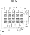
- FIGS. 5A to 5L are sectional views illustrating a manufacturing method of a semiconductor memory device in accordance with an embodiment of the present disclosure.
- a preliminary memory cell array 110 formed through the process ST 1 , shown in FIG. 4 may be supported by a support structure 101 .
- the preliminary memory cell array 110 may include a stack structure ST and cell pillars CP.
- the stack structure ST may be disposed between vertical insulating layers 133 .
- the stack structure ST may include a first surface SU 1 that faces the support structure 101 and a second surface SU 2 that faces the opposite direction compared to the first surface SU 1 .
- the stack structure ST may include interlayer insulating layers 111 and conductive layer 117 , which are alternately stacked on the support structure 101 .
- the interlayer insulating layers 111 and the conductive layers 117 may extend in the first direction D 1 and the second direction D 2 .
- the interlayer insulating layers 111 and the conductive layers 117 may be disposed at levels that are spaced apart from the support structure 101 at different distances.
- Each of the conductive layers 117 may include a single conductive material or two or more different conductive materials.
- each of the conductive layers 117 may include a metal barrier layer 113 and a metal layer 115 .
- the metal barrier layer 113 may be disposed between each of the cell pillars CP and the metal layer 115 .
- the metal barrier layer 113 may extend between each of the interlayer insulating layers 111 and the metal layer 115 .
- the embodiment of the present disclosure is not limited thereto, and the conductive material of each of the conductive layers 117 may vary.
- Each of the cell pillars CP may include a first part CP[ 1 ] that penetrates the stack structure ST and a second part CP[ 2 ] that extends in the third direction D 3 toward the support structure 101 from the first part CP[ 1 ].
- the second part CP[ 2 ] may be inserted into a groove 100 that is formed in the support structure 101 .
- the support structure 101 may be a silicon substrate with the groove 100 .
- Each of the cell pillars CP may include a memory layer 121 , a channel layer 123 , and a core insulating layer 125 .
- the core insulating layer 125 may be disposed in a central region of the cell pillar CP. In other words, the core insulating layer 125 may be disposed in a central region of the first part CP[ 1 ] and may extend to a central region of the second part CP[ 2 ].
- the channel layer 123 may surround a sidewall of the core insulating layer 125 and may extend along a bottom surface of the core insulating layer 125 that faces the third direction D 3 .
- the memory layer 121 may extend along an outer wall of the channel layer 123 that faces the support structure 101 and the stack structure ST.
- the channel layer 123 may include a semiconductor layer to provide a channel region of each of the memory cell strings MS 1 and MS 2 , shown in FIG. 1 .
- the channel layer 123 may include silicon.
- the memory layer 121 may include a blocking insulating layer 121 A, a data storage layer 121 B, and a tunnel insulating layer 121 C, which are shown in FIG. 6A .
- the preliminary memory cell array 110 may be formed through various processes.
- the process of forming the preliminary memory cell array 110 may include a process of alternately stacking first material layers and second material layers on the support structure 101 , a process of forming a hole 120 that penetrates the first material layers and the second material layers, a process of forming the groove 100 by etching the support structure 101 through the hole 120 , a process of forming the cell pillar CP that fills the hole 120 and extends into the groove 100 , and a process of forming a slit 131 that penetrates the first material layers and the second material layers.
- the first material layers may be the interlayer insulating layers 111
- the second material layers may be selected from materials with an etch selectivity with respect to the interlayer insulating layers 111 .
- the interlayer insulating layers 111 may include silicon oxide, and a material with an etch selectivity with respect to the silicon oxide may be silicon nitride.
- the second material layers that are formed of the silicon nitride may be replaced with the conductive layers 117 through the slit 131 . After the second material layers are replaced with the conductive layers 117 , the slit 131 may be filled with the vertical insulating layer 133 .
- an isolation layer 135 may be formed, which penetrates some of the conductive layers 117 , shown in FIG. 5A .
- the isolation layer 135 may penetrate at least one conductive layer among the conductive layers 117 that is adjacent to the second surface SU 2 of the stack structure ST, shown in FIG. 5A .
- the conductive layer that is penetrated by the isolation layer 135 may be isolated into first select lines 117 S 1 .
- the isolation layer 135 may extend in the second direction D 2 and may be formed of an insulating material. First select lines 117 S 1 that are disposed at the same level may be insulated from each other by the isolation layer 135 .
- the first select lines 117 S 1 may constitute the drain select lines or source select lines.
- first select lines 117 S 1 constitute source select lines.
- a recess region 141 that exposes a portion of an inner wall of the channel layer 123 may be defined by etching a portion of the core insulating layer 125 of the cell pillar CP.
- a source layer 140 may be formed, which is connected to the channel layer 123 of the cell pillar CP.
- the source layer 140 may include a doped semiconductor layer 143 and a conductive layer with a metal.
- the conductive layer with the metal may include a metal barrier layer 145 and a metal layer 147 .
- the doped semiconductor layer 143 may include a pillar part 143 A that fills the recess region 141 , shown in FIG. 5C , and a horizontal part 143 B that extends from the pillar part 143 A.
- the pillar part 143 A may be in contact with the channel layer 123 and may be surrounded by the channel layer 123 .
- the horizontal part 143 B may extend to cover the stack structure ST and the vertical insulating layer 133 .
- the doped semiconductor layer 143 may include at least one of an n-type impurity and a p-type impurity.
- the doped semiconductor layer 143 may include an n-type doped silicon layer.
- the metal barrier layer 145 may be formed between the doped semiconductor layer 143 and the metal layer 147 .
- a first insulating layer 149 may be formed on the metal layer 147 .
- the first insulating layer 149 may extend to cover the metal layer 147 .
- a peripheral circuit structure 170 may be disposed to face the first insulating layer 149 .
- the peripheral circuit structure 170 may include a substrate 151 with transistors 150 , an insulating structure 161 that covers the substrate 151 , an interconnection structure 163 , and a second insulating layer 169 .
- the substrate 151 may be a semiconductor substrate such as a silicon substrate or a germanium substrate.
- Each of the transistors 150 may be formed in an active region of the substrate 151 , which is partitioned by isolation layers 153 .
- Each of the transistors 150 may include a gate insulating layer 157 that is disposed on the active region, a gate electrode 159 that is disposed on the gate insulating layer 157 , and junctions 155 that are formed in the active region at both sides of the gate electrode 159 .
- the transistors 150 may constitute a peripheral circuit that controls an operation of memory cell strings.
- the insulating structure 161 may include two or more insulating layers.
- the interconnection structure 163 may be buried in the insulating structure 161 and may be connected to the transistors 150 .
- the second insulating layer 169 may be disposed on the insulating structure 161 .
- the peripheral circuit structure 170 may be bonded to the first insulating layer 149 .
- the second insulating layer 169 of the peripheral circuit structure 170 may be bonded to the first insulating layer 149 .
- the support structure 101 shown in FIG. 5E , may be removed. Accordingly, the second part CP[ 2 ] of the cell pillar CP may be exposed.
- the memory layer 121 of the cell pillar CP may serve as an etch stop layer.
- the support structure 101 may be removed so that the uneven structure that is described with reference to the process ST 5 , shown in FIG. 4 , is defined by the second part CP[ 2 ] of the cell pillar CP.
- the second part CP[ 2 ] of the cell pillar CP may protrude farther in the third direction D 3 than the stack structure ST, and therefore, the uneven structure may be defined.
- n-type and p-type impurities may be injected into a partial region of the channel layer 123 that constitutes the second part CP[ 2 ] of each of the cell pillars CP.
- an impurity injection region 123 N may be formed in a partial region of the channel layer 123 of each of the cell pillars CP by injecting an n-type impurity into the channel layer 123 .
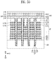
- a protective layer 181 may be formed.
- the protective layer 181 may cover the second part CP[ 2 ] of each of the cell pillars CP.
- the protective layer 181 may include a material with an etch selectivity with respect to the interlayer insulating layers 111 and the conductive layers 117 .
- the protective layer 181 may include an amorphous carbon layer.
- the protective layer 181 may have an overhang structure.
- the deposition thickness of the protective layer 181 may be controlled such that a space between the cell pillars CP might not be completely filled by the protective layer 181 .
- the protective layer 181 may be deposited such that a first opening 183 is defined in the space between the cell pillars CP by the protective layer 181 .
- the first opening 183 may be defined between a first inclined surface S 1 and a second inclined surface S 2 of the protective layer 181 , which face each other between cell pillars CP.
- the width WA of the first opening 183 may narrow as the first opening 183 moves farther from the stack structure, due to the protective layer 181 with the overhang structure.
- the protective layer 181 may include a shielding pattern 181 A, a protrusion pattern 181 B, and a horizontal pattern 181 C.
- the protrusion pattern 181 B and the horizontal pattern 181 C may extend from the shielding pattern 181 A.
- the shielding pattern 181 A may be a portion of the protective layer 18 that surrounds a sidewall SW of the second part CP[ 2 ] of the cell pillar CP.
- the second part CP[ 2 ] of the cell pillar CP may include a surface SU 3 that faces the third direction D 3 .
- the protrusion pattern 181 B may be a portion of the protective layer 181 disposed on the surface SU 3 of the second part CP[ 2 ].
- the width of the protrusion pattern 181 B may widen as the protrusion pattern 181 B moves farther from the second part CP[ 2 ].
- the first width W 1 of the protrusion pattern 181 B that is adjacent to the second part CP[ 2 ] may be formed to be narrower than the second width W 2 at an upper end of the protrusion pattern 181 B.
- the overhang structure may be defined.
- the horizontal pattern 181 C may be a portion of the protective layer 181 that overlaps with the stack structure ST between the first inclined surface S 1 and the second inclined surface S 2 . Because the protective layer 181 is deposited under the condition in which the step coverage is poor, a thickness D 1 of the protrusion pattern 181 that is deposited on the surface SU 3 of the second part CP[ 2 ] may be thicker than that D 2 of the horizontal pattern 181 C that is deposited on the first surface SU 1 of the stack structure ST.
- a mask pattern 185 may be formed on the protective layer 181 by using a photolithography process.
- the mask pattern 185 may be a photoresist pattern.
- the mask pattern 185 may include a second opening 187 .
- the second opening 187 may extend in the second direction D 2 .
- the second opening 187 may overlap with the first opening 183 .
- the second opening 187 may expose the first opening 183 , which overlaps with the isolation layer 135 .
- the embodiment of the present disclosure is not limited thereto, and the position and shape of the second opening 187 may vary.
- the width WB of the second opening 187 may be formed to be wider than the width WA of the first opening 183 .
- a sidewall 187 S of the second opening 187 may overlap with the protrusion pattern 181 B.
- the conductive layer 117 around the cell pillars CP may be blocked by the shielding pattern 181 A and the protrusion pattern 181 B of the protective layer 181 . Accordingly, although the width WB of the second opening 187 is formed to be wider than the width WA of the first opening 183 , a partial region of the conductive layer 117 around the cell pillars CP may be protected from a subsequent etching process through the protective layer 181 .
- the mask pattern 185 may be formed even when a high-resolution exposure apparatus is not used.
- a slit 189 may be formed by etching a portion of the stack structure ST through the second opening 187 and the first opening 183 .
- the slit 189 may extend in the second direction D 2 .
- At least one conductive layer among the conductive layers 117 of the stack structure ST that is adjacent to the first opening 183 , shown in FIG. 5H , may be isolated into second select lines 117 S 2 by the slit 189 .
- the second select lines 117 S 2 may constitute drain select lines.
- Conductive layers between the isolation layer 135 and the slit 189 may constitute word line 117 W.
- the word lines 117 W may extend to overlap with the isolation layer 135 and the slit 189 .
- a portion of the protective layer 181 may be etched during an etching process for forming the slit 189 .
- the protective layer 181 with the overhang structure having different thicknesses and different widths with respect to regions as described with reference to FIG. 5G , may remain with a width W 3 decreased between the sidewall SW of the cell pillar CP and the first opening 183 . More specifically, a partial region of the protective layer 181 that is exposed by the second opening 187 might not be completely removed, but may remain with a decreased width W 3 .
- a partial region of the protective layer 181 that remains between the sidewall SW of the cell pillar CP and the first opening 183 may protect the conductive layer 117 from the etching process.
- the second select line 117 S 2 may remain between the slit 189 and the sidewall SW of the cell pillar CP, and thus, a select transistor with a gate all around (GAA) structure may be defined as described with reference to FIG. 3A .
- GAA gate all around
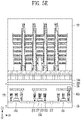
- the protective layer 181 and the mask pattern 185 may be removed such that cell pillars CP may be exposed.
- an upper insulating layer 191 may be formed.
- the upper insulating layer 191 may extend to fill the slit 189 between the second select lines 117 S 2 and to cover the second part CP[ 2 ] of each of the cell pillars CP.
- the surface of the upper insulating layer 191 may be planarized through a process, such as Chemical Mechanical Polishing (CMP).
- CMP Chemical Mechanical Polishing
- a bit line contact 197 may be formed, which is in contact with the channel layer 123 of the cell pillar CP.
- the process of forming the bit line contact 197 may include a process of forming a contact hole 190 that penetrates the upper insulating layer 191 and the memory layer 121 and a process of filling the contact hole 190 with a conductive material.
- the conductive material that constitutes the bit line contact 197 may vary.
- the bit line contact 197 may include a metal barrier layer 193 and a metal layer 195 .
- the metal barrier layer 193 may extend along a surface of the contact hole 190 and may be in contact with the channel layer 123 .
- the metal layer 195 may be disposed on the metal barrier layer 193 .
- a bit line 205 that is in contact with the bit line contact 197 may be formed on the upper insulating layer 191 .
- the bit line 205 may overlap with the peripheral circuit structure 170 , the stack structure ST being interposed therebetween.
- the conductive material of the bit line 205 may vary.
- the bit line 205 may include a metal barrier layer 201 and a metal layer 203 .
- the metal barrier layer 201 may extend to be in contact with the bit line contact 197 and to overlap with the upper insulating layer 191 .
- the metal layer 203 may be disposed on the metal barrier layer 201 .
- the cell pillars CP may include cell pillars that are connected to the bit line 205 , shown in the drawings, and cell pillars that are connected to another bit line, which is not shown in the drawings. Some of the cell pillars CP, which are not connected to the bit line 205 , may be connected to another bit line, which is not shown in the drawings via bit line contacts, which are not shown in the drawings.
- FIGS. 6A to 6C are sectional views illustrating an embodiment of the process of forming the impurity injection region shown in FIG. 5F .
- FIGS. 6A to 6C are enlarged sectional views of region A shown in FIG. 5F .
- the blocking insulating layer 121 A of the memory layer 121 may be exposed.
- the blocking insulating layer 121 A, the data storage layer 121 B, and the tunnel insulating layer 121 C of the memory layer 121 may be made of the same materials as the blocking insulating layer 63 , the data storage layer 65 , and the tunnel insulating layer 67 , which are described with reference to FIG. 3A .
- a partial region of the blocking insulating layer 121 A that is surrounded by the stack structure ST might not be exposed, but may be protected by the stack structure ST.
- the exposed region of the blocking insulating layer 121 A may be selectively removed.
- the exposed region of the blocking insulating layer 121 A may be removed through wet etching. Accordingly, a partial region of the data storage layer 121 B may be exposed.
- the impurity injection region 123 N may be formed in the partial region of the channel layer 123 .
- the impurity injection region 123 N may be formed by injecting an n-type impurity 122 into the partial region of the channel layer 123 .
- FIGS. 7A to 7H are sectional views illustrating a manufacturing method of a semiconductor memory device in accordance with an embodiment of the present disclosure.
- a preliminary memory cell array 310 that is formed through the process ST 1 , shown in FIG. 4 , may be supported by a support structure 305 .
- the preliminary memory cell array 310 may include a stack structure ST′ and cell pillars CP′.
- the support structure 305 may include a silicon substrate 301 that overlaps with the stack structure ST′ and an etch stop layer 303 that is disposed between the stack structure ST′ and the silicon substrate 301 .
- the etch stop layer 303 may include a material with an etch selectivity with respect to the silicon substrate 301 .
- the etch stop layer 303 may include a nitride layer.
- the stack structure ST′ may be disposed between vertical insulating layers 333 .
- the stack structure ST′ may include conductive layers 309 , 317 , and 317 S 1 and interlayer insulating layers 311 , which are alternately stacked on the support structure 305 .
- the conductive layers 309 , 317 , and 317 S 1 and the interlayer insulating layers 311 may extend in the first direction D 1 and the second direction D 2 .
- the conductive layers 309 , 317 , and 317 S 1 and the interlayer insulating layers 311 may be disposed at levels that are spaced apart from the support structure 305 at different distances.
- Each of the conductive layers 309 , 317 , and 317 S 1 may include various conductive materials, such as a metal layer, a metal silicide layer, and a doped silicon layer.
- the conductive layers 309 , 317 , and 317 S 1 may include a first conductive layer 307 that is adjacent to the support structure 305 and second conductive layers 317 and 317 S 1 that are stacked on the first conductive layer 309 to be spaced apart from each other.
- the first conductive layer 309 may include doped silicon.
- Each of the second conductive layers 317 and 317 S 1 may include a metal barrier layer 313 and a metal layer 315 , similarly to the conductive layer 117 , shown in FIG. 5A .
- Each of the cell pillars CP′ may include a first part CP′[ 1 ] that penetrates the stack structure ST′ and a second part CP′[ 2 ] that extends in the third direction D 3 toward the support structure 305 from the first part CP′[ 1 ].
- the second part CP′[ 2 ] may be inserted into a groove 300 that is formed in the etch stop layer 303 .
- Each of the cell pillars CP′ may include a memory layer 321 , a channel layer 323 , a core insulating layer 325 , and a doped semiconductor pattern 327 .
- the first part CP′[ 1 ] of the cell pillar CP′ may include a central region that is filled with the core insulating layer 325 and the doped semiconductor pattern 327 .
- the core insulating layer 325 may extend to a central region of the second part CP′[ 2 ].
- the doped semiconductor pattern 327 may overlap with the core insulating layer 325 .
- the doped semiconductor pattern 327 may include at least one of n-type and p-type impurities. In an embodiment, the doped semiconductor pattern 327 may include an n-type doped silicon layer.
- the channel layer 323 may extend to surround a sidewall of the core insulating layer 325 and to surround a sidewall of the doped semiconductor pattern 327 .
- the channel layer 323 may extend along a bottom surface of the core insulating layer 325 , which faces the third direction D 3 .
- the memory layer 321 may extend along an outer wall of the channel layer 323 , which faces the support structure 305 and the stack structure ST′.
- the channel layer 323 may include a semiconductor layer.
- the memory layer 321 may include the blocking insulating layer 53 , the data storage layer 65 , and the tunnel insulating layer 67 , which are shown in FIG. 3A .
- the preliminary memory cell array 310 may be formed through various processes.
- the preliminary memory cell array 310 may be formed by using the embodiment, described with reference to FIG. 5A .
- At least one of the conductive layers 317 and 317 S 1 may constitute first select lines 317 S 1 that are spaced apart from each other by an isolation layer 335 as described with reference to FIG. 5B .
- the first select lines 317 S 1 may constitute drain select lines or source select lines.
- FIGS. 7B to 7H subsequent processes will be described with reference to FIGS. 7B to 7H .
- the present disclosure is not limited thereto.
- a bit line contact 345 may be formed, which is connected to the channel layer 323 of the cell pillar CP′.
- the process of forming the bit line contact 345 may include a process of forming a first insulating layer 337 that extends to cover the cell pillar CP′ and the cell structure ST′, a process of forming a contact hole 340 that penetrates the first insulating layer 337 and opens the doped semiconductor pattern 327 , and a process of filling the contact hole 340 with a conductive material.
- the conductive material that constitutes the bit line contact 345 may include a metal barrier layer 341 and a metal layer 343 .
- the metal barrier layer 341 may extend along a surface of the contact hole 340 and may be in contact with the doped semiconductor pattern 327 .
- the metal layer 343 may be disposed on the metal barrier layer 341 .
- bit line 351 may be formed, which is in contact with the bit line contact 345 .
- the bit line 351 may extend onto the first insulating layer 337 .
- the conductive material of the bit line 351 may vary.
- the bit line 351 may include a metal barrier layer 347 and a metal layer 349 .
- the metal barrier layer 347 may be in contact with the bit line contact 345 and may extend to overlap with the first insulating layer 337 .
- the metal layer 349 may be disposed on the metal barrier layer 347 .
- the cell pillars CP′ may include cell pillars that are connected to the bit line 351 , shown in the drawing, and cell pillars that are connected to another bit line, which is not shown in the drawing. Some of the cell pillars CP′, which are not connected to the bit line 351 , may be connected to another bit line, which is not shown in the drawing, via bit line contacts, which are not shown in the drawing.
- a first insulating structure 353 may be formed on the bit line 351 .
- a first interconnection structure 355 may be buried in the first insulating structure 353 .
- the first insulating structure 353 may include two or more insulating layers.
- the first interconnection structure 355 may include a conductive material of various shapes and various types.
- the first interconnection structure 355 may include a first bonding metal pattern 355 B.
- the first interconnection structure 355 may overlap with the stack structure ST′, the bit line 351 being interposed therebetween.
- a peripheral circuit structure 370 may be disposed to face the first bonding metal pattern 355 B. Similar to what has been described with reference to FIG. 5E , the peripheral circuit structure 370 may include a substrate 361 with active regions that are partitioned by isolation layers 363 and transistors 360 that are formed in the active regions, a second insulating structure 365 that covers the substrate 361 , and a second interconnection structure 367 .
- the second interconnection structure 367 may include a conductive material of various shapes and various types.
- the second interconnection structure 367 may include a second bonding metal pattern 367 B.
- the peripheral circuit structure 370 may be bonded to the first interconnection structure 355 .
- the second insulating structure 365 of the peripheral circuit structure 370 may be bonded to the first insulating structure 353
- the second bonding metal pattern 367 B of the peripheral circuit structure 370 may be bonded to the first bonding metal pattern 355 B.
- the support structure 305 may be removed. While the silicon substrate 301 , shown in FIG. 7C , is removed, the stack structure ST′ may be protected by the etch stop layer 303 , shown in FIG. 7C . While the etch stop layer 303 of the support structure 305 , shown in FIG. 7C , is removed, the first conductive layer 309 may serve as an etch stop layer.
- the second part CP′[ 2 ] of the cell pillar CP′ may be exposed.
- the uneven structure that is described with reference to the process ST 5 , shown in FIG. 4 may be defined by the exposed second part CP′[ 2 ] of the cell pillar CP′.
- a protective layer 381 may be formed.
- the protective layer 381 may have an overhang structure, which covers the second part CP′[ 2 ] of each of the cell pillars CP′ and defines a first opening 383 , similar to what has been described with reference to FIG. 5G .
- a mask pattern 385 with a second opening 387 may be formed.
- a slit 389 may be formed by etching a portion of the stack structure ST′, shown in FIG. 7D , through the second opening 387 and the first opening 383 .
- the slit 389 may be formed to penetrate the first conductive layer 309 , shown in FIG. 7D .
- the first conductive layer 309 shown in FIG. 7D , may be isolated into second select lines 309 S 2 by the slit 389 .
- the second select lines 309 S 2 may constitute source select lines.
- Conductive layers between the second select line 309 S 2 and the first select line 31751 may constitute word lines 317 W.
- the word lines 317 W may extend to overlap with the isolation layer 335 and the slit 389 .
- the protective layer 381 and the mask pattern 385 which are shown in FIG. 7E , may be removed such that the cell pillars CP′ may be exposed. Subsequently, an upper insulating layer 391 may be formed. The upper insulating layer 391 may extend to fill the slit 389 between the second select lines 309 S 2 and to cover the second part CP′[ 2 ] of each of the cell pillars CP′.
- a portion of the upper insulating layer 391 and a portion of the memory layer 321 may be removed through an etching process, such as an etch-back process, such that the channel layer 323 of each of the cell pillars CP′ may be exposed.
- a source layer 399 may be formed.
- the source layer 399 may be connected to the channel layer 323 of each of the cell pillars CP′.
- the source layer 399 may include a doped semiconductor layer 393 and a conductive layer with a metal.
- the conductive layer with the metal may include a metal barrier layer 395 and a metal layer 397 .
- the doped semiconductor layer 393 may be in contact with the channel layer 323 .
- the doped semiconductor layer 393 may include at least one of n-type and p-type impurities.
- the doped semiconductor layer 393 may include an n-type doped silicon layer.
- the metal barrier layer 395 may be formed between the doped semiconductor layer 393 and the metal layer 309 .
- FIG. 8 is a block diagram illustrating a configuration of a memory system 1100 in accordance with an embodiment of the present disclosure.
- the memory system 1100 includes a memory device 1120 and a memory controller 1110 .
- the memory device 1120 may include a memory cell array and a peripheral circuit structure, which are coupled to each other through bonding, and may include select transistors that are adjacent to the peripheral circuit structure.
- the select transistors may be connected to select lines that are isolated by a slit.
- Each of the select transistors may have a gate all around (GAA) structure.
- GAA gate all around
- the memory device 1120 may be a multi-chip package configured with a plurality of flash memory chips.
- the memory controller 1110 may control the memory device 1120 and may include a Static Random Access Memory (SRAM) 1111 , a Central Processing Unit (CPU) 1112 , a host interface 1113 , an error correction block 1114 , and a memory interface 1115 .
- the SRAM 1111 may be used as an operation memory of the CPU 1112
- the CPU 1112 may perform overall control operations for data exchange of the memory controller 1110
- the host interface 1113 may include a data exchange protocol for a host that is connected with the memory system 1100 .
- the error correction block 1114 may detect and correct an error that is included in a data that is read from the memory device 1120 .
- the memory interface 1115 may interface with the memory device 1120 .
- the memory controller 1110 may further include a Read Only Memory (ROM) for storing code data for interfacing with the host, and the like.
- ROM Read Only Memory
- FIG. 9 is a block diagram illustrating a configuration of a computing system 1200 in accordance with an embodiment of the present disclosure.
- the computing system 1200 may include a CPU 1220 , a random access memory (RAM) 1230 , a user interface 1240 , a modem 1250 , and a memory system 1210 , which are electrically connected to a system bus 1260 .
- the computing system 1200 may be a mobile device.
- the memory system 1210 may be configured with a memory device 1212 and a memory controller 1211 .
- the memory device 1212 may include a memory cell array and a peripheral circuit structure, which are coupled to each other through bonding, and may include select transistors that are adjacent to the peripheral circuit structure.
- the select transistors may be connected to select lines that are isolated by a slit.
- Each of the select transistors may have a gate all around (GAA) structure.
- GAA gate all around
- a select transistor which is defined at an intersection portion of a select line and a cell pillar, may be formed in a gate all around (GAA) structure, so that operational characteristics of the semiconductor memory device may be improved.
- GAA gate all around
Landscapes
- Semiconductor Memories (AREA)
- Non-Volatile Memory (AREA)
- Chemical & Material Sciences (AREA)
- Chemical Kinetics & Catalysis (AREA)
- General Chemical & Material Sciences (AREA)
Abstract
Description
- The present application claims priority under 35 U.S.C. § 119(a) to Korean patent application number 10-2020-0129527, filed on Oct. 7, 2020, in the Korean Intellectual Property Office, the entire disclosure of which is incorporated herein by reference.
- The present disclosure may generally relate to a manufacturing method of a semiconductor memory device, and more particularly, to a manufacturing method of a three-dimensional semiconductor memory device.
- A semiconductor memory device includes a plurality of memory cells capable of storing data. The memory cells may be three-dimensionally arranged to implement a three-dimensional semiconductor memory device. The memory cells may constitute a plurality of memory cell strings. The memory cell strings may be connected to word lines and select lines.
- In an embodiment of the present disclosure, there may be provided a method of manufacturing a semiconductor memory device, the method including: forming a preliminary memory cell array on a support structure, the preliminary memory cell array with a stack structure and cell pillars; removing the support structure to expose a portion of each of the cell pillars; forming a protective layer that covers the exposed portion of each of the cell pillars; forming a mask pattern that exposes an opening defined between inclined surfaces of the protective layer, wherein the inclined surfaces are disposed between the cell pillars; and etching at least one conductive layer among the conductive layers that is adjacent to the opening, thereby isolating the at least one conductive layer into select lines.
- Examples of embodiments will now be described hereinafter with reference to the accompanying drawings; however, they may be embodied in different forms and should not be construed as limited to the embodiments set forth herein.
- In the drawing figures, dimensions may be exaggerated for clarity of illustration. It will be understood that when an element is referred to as being “between” two elements, it can be the only element between the two elements, or one or more intervening elements may also be present. Like reference numerals refer to like elements throughout.
-
FIG. 1 is a circuit diagram illustrating a memory block of a semiconductor memory device in accordance with an embodiment of the present disclosure. -
FIGS. 2A and 2B are perspective views illustrating semiconductor memory devices in accordance with embodiments of the present disclosure. -
FIG. 3A illustrates a layout of a gate stack structure and channel structures of a semiconductor memory device in accordance with an embodiment of the present disclosure, andFIG. 3B illustrates a layout of bit lines. -
FIG. 4 is a flowchart schematically illustrating a manufacturing method of a semiconductor memory device in accordance with an embodiment of the present disclosure. -
FIGS. 5A to 5L are sectional views illustrating a manufacturing method of a semiconductor memory device in accordance with an embodiment of the present disclosure. -
FIGS. 6A to 6C are sectional views illustrating an embodiment of a process of forming an impurity injection region shown inFIG. 5F . -
FIGS. 7A to 7H are sectional views illustrating a manufacturing method of a semiconductor memory device in accordance with an embodiment of the present disclosure. -
FIG. 8 is a block diagram illustrating a configuration of a memory system in accordance with an embodiment of the present disclosure. -
FIG. 9 is a block diagram illustrating a configuration of a computing system in accordance with an embodiment of the present disclosure. - Specific structural or functional descriptions disclosed herein are merely illustrative for the purpose of describing embodiments according to the concept of the present disclosure. The embodiments according to the concept of the present disclosure can be implemented in various forms, and should not be construed as limited to the specific embodiments set forth herein.
- Hereinafter, the terms ‘first’ and ‘second’ are used to distinguish one component from another component. The terms may be used to describe various components, but the components are not limited by the terms. Same reference numerals refer to same elements throughout the specification. Thus, even though a reference numeral is not mentioned or described with reference to a drawing, the reference numeral may be mentioned or described with reference to another drawing. In addition, even though a reference numeral is not shown in a drawing, it may be mentioned or described with reference to another drawing.
- Embodiments may provide a manufacturing method of a semiconductor memory device, which can improve operational characteristics of the semiconductor memory device.
-
FIG. 1 is a circuit diagram illustrating a memory block BLK of a semiconductor memory device in accordance with an embodiment of the present disclosure. - Referring to
FIG. 1 , the semiconductor memory device may include the memory block BLK. The memory block BLK may include a plurality of memory cell strings MS1 and MS2 that are connected to a source layer SL and a plurality of bit lines BL. - Each of the memory cell strings MS1 and MS2 may include a plurality of memory cells MC that are connected in series, at least one source select transistor SST, and at least one drain select transistor DST. In an embodiment, each of the memory cell strings MS1 and MS2 may include one source select transistor SST that is connected between the plurality of memory cells MC and the source layer SL. In another embodiment, each of the memory cell strings MS1 and MS2 may include two or more source select transistors SST that are connected in series between the plurality of memory cells MC and the source layer SL. In an embodiment, each of the memory cell strings MS1 and MS2 may include one drain select transistor DST that is connected between the plurality of memory cells MC and a bit line BL. In another embodiment, each of the memory cell strings MS1 and MS2 may include two or more drain select transistors DST that are connected in series between the plurality of memory cells MC and the bit line BL.
- The plurality of memory cells MC may be connected to the source layer SL via the source select transistor SST. The plurality of memory cells MC may be connected to the bit line BL via the drain select transistor DST.
- Gates of source select transistors SST that are disposed at the same level may be connected to source select lines SSL1 and SSL2 isolated from each other. Gates of drain select transistors DST that are disposed at the same level may be connected to drain select lines DSL1 and DSL2 that are isolated from each other. Gates of the memory cells MC may be respectively connected to a plurality of word lines WL. The word lines WL may be disposed at different levels, and gates of memory cells MC that are disposed at the same level may be connected to a single word line WL.
- The memory block BLK with a first source select line SSL1 and a second source select line SSL2 that are isolated from each other at the same level and a first drain select line DSL1 and a second drain select line DSL2 that are isolated from each other at the same level is exemplified in the drawing. However, the present disclosure is not limited thereto. In an embodiment, the memory block BLK may include three or more source select lines that are isolated from one another at the same level. Similarly, the memory block BLK may include three or more drain select lines that are isolated from one another at the same level.
- The plurality of memory cell strings MS1 and MS2 may be connected to each of the word lines WL. The plurality of memory cell strings MS1 and MS2 may include a first group and a second group, which can be individually selected by the first source select line SSL1 and the second source select line SSL2. The first group may include first memory cell strings MS1, and the second group may include second memory cell strings MS2.
- Memory cells MC of the first memory cell strings MS1 may be respectively connected to the bit lines BL via drain select transistors DST that are connected to first drain select lines DSL1. Memory cells MC of the second memory cell strings MS2 may be respectively connected to the bit lines BL via drain select transistor DST that is connected to second drain select lines DSL2. One of the first memory cell strings MS1 and one of the second memory cell strings MS2 may be connected to a single bit line BL.
- The memory cells MC of the first memory cell strings MS1 may be connected to the source layer SL based on a gate signal applied to the first source select line SSL. The memory cells MC of the second memory cell strings MS2 may be connected to the source layer SL based on a gate signal to the second source select line SSL2. Accordingly, the plurality of memory cell strings MS1 and MS2 may be isolated into groups that can be individually and simultaneously selected for each of the source select lines SSL1 and SSL2 in a read operation or a verify operation. In an embodiment, in the read operation or the verify operation, one of the first source select line SSL1 and a second source select line SSL2 may be selected so that one group of the first group of the first memory cell strings MS1 and the second group of the second memory cell strings MS2 may be connected to the source layer SL. Accordingly, in the embodiment of the present disclosure, channel resistance may be reduced as compared with a case in which the first memory cell strings MS1 and the second memory cell strings MS2 are simultaneously connected to the source layer SL in the read operation or the verify operation. Thus, in the embodiment of the present disclosure, read disturb may be reduced.
-
FIGS. 2A and 2B are perspective views illustratingsemiconductor memory devices FIGS. 2A and 2B illustrate a portion of a configuration of each of thesemiconductor memory devices semiconductor memory devices - Referring to
FIGS. 2A and 2B , each of thesemiconductor memory devices peripheral circuit structure memory cell array 5A to 5B, asource layer bit lines - The
peripheral circuit structure peripheral circuit structure memory cell array memory cell array memory cell array peripheral circuit structure peripheral circuit structure memory cell array peripheral circuit structure - The
memory cell array 5A or may overlap with theperipheral circuit structure memory cell array source layer bit lines - A direction, perpendicular to a plane that extends in the first direction D1 and the second direction D2, is defined as a third direction D3. The arrangement of the
memory cell array source layer bit lines - Referring to
FIG. 2A , thememory cell array 5A may overlap with theperipheral circuit structure 10A, thesource layer 20A being interposed therebetween. The plurality ofbit lines 80A may overlap with theperipheral circuit structure 10A, thesource layer 20A, and thememory cell array 5A, thesource layer 20A and thememory cell array 5A being interposed between the plurality ofbit lines 80A and theperipheral circuit structure 10A. - The
memory cell array 5A may include channel structures 60A1 and 60A2 and agate stack structure 90A that surrounds the channel structures 60A1 and 60A2. - The
gate stack structure 90A may include source select lines 31A1, 31A2, 32A1, and 32A2, word lines 40A, and drain select lines 51A1, 51A2, 52A1, and 52A2. The source select lines 31A1, 31A2, 32A1, and 32A2, the word lines 40A, and the drain select lines 51A1, 51A2, 52A1, and 52A2 may be disposed to be spaced apart from each other. Conductive materials that constitute the source select lines 31A1, 31A2, 32A1, and 32A2, the word lines 40A, and the drain select lines 51A1, 51A2, 52A1, and 52A2 may vary. In an embodiment, the source select lines 31A1, 31A2, 32A1, and 32A2 and the drain select lines 51A1, 51A2, 52A1, and 52A2 may be formed of the same conductive material as the word lines 40A. However; the present disclosure is not limited thereto. In another embodiment, the source select lines 31A1, 31A2, 32A1, and 32A2 or the drain select lines 51A1, 51A2, 52A1, and 52A2 may be formed of a conductive material that is different from that constituting the word lines 40A. - The source select lines 31A1, 31A2, 32A1, and 32A2 may be disposed between the
source layer 20A and the plurality ofbit lines 80A. The source select lines 31A1, 31A2, 32A1, and 32A2 may include at least one first source select line and at least one second source select line. In an embodiment, the source select lines 31A1, 31A2, 32A1, and 32A2 may include two first source select lines 31A1 and 32A1 and two second source select lines 31A2 and 32A2. The first source select lines 31A1 and 32A1 may include a first source select line 31A1 of a first level and a first source select line 32A1 of a second level, which are spaced apart from each other in the third direction D3. The second source select lines 31A2 and 32A2 may include a second source select line 31A2 of the first level and a second source select line 32A2 of the second level, which are spaced apart from each other in the third direction D3. The first source select line 31A1 of the first level and the second source select line 31A2 of the first level may be spaced apart from each other in the first direction D1. The first source select line 32A1 of the second level and the second source select line 32A2 of the second level may be spaced apart from each other in the first direction D1. - The drain select lines 51A1, 51A2, 52A1, and 52A2 may be disposed between the source select lines 31A1, 31A2, 32A1, and 32A2 and the plurality of
bit lines 80A. The drain select lines 51A1, 51A2, 52A1, and 52A2 may include at least one first drain select line and at least one second drain select line. In an embodiment, the drain select lines 51A1, 51A2, 52A1, and 52A2 may include two first drain select lines 51A1 and 52A1 and two second drain select lines 51A2 and 52A2. The first drain select lines 51A1 and 52A1 may include a first drain select line 51A1 of a third level and a first drain select line 52A1 of a fourth level, which are spaced apart from each other in the third direction D3. The second drain select lines 51A2 and 52A2 may include a second drain select line 51A2 of the third level and a second drain select line 52A2 of the fourth level, which are spaced apart from each other in the third direction D3. The first drain select line 51A1 of the third level and the second drain select line 51A2 of the third level may be spaced apart from each other in the first direction D1. The first drain select line 52A1 of the fourth level and the second drain select line 52A2 of the fourth level may be spaced apart from each other in the first direction D1. - Each of the word lines 40A may be disposed between the first source select lines 31A1 and 32A1 and the first drain select lines 51A1 and 52A1, and may extend between the second source select lines 31A2 and 32A2 and the second drain select lines 51A2 and 52A2. The word lines 40A may be stacked to be spaced apart from each other in the third direction D3.
- The channel structures 60A1 and 60A2 may include a channel layer that is used as a channel region of the memory cell strings MS1 and MS2, shown in
FIG. 1 . The channel structures 60A1 and 60A2 may be in contact with thesource layer 20A. The channel structures 60A1 and 60A2 may penetrate thegate stack structure 90A and may extend toward thebit lines 80A. The channel structures 60A1 and 60A2 may be connected to thebit lines 80A via bit line contacts 70A1 and 70A2. - The channel structures 60A1 and 60A2 may include a first channel structure 60A1 that is controlled by the first source select lines 31A1 and 32A1 and a second channel structure 60A2 that is controlled by the second source select lines 31A2 and 32A2. The first channel structure 60A1 may penetrate the first drain select lines 51A and 52A1, the word lines 40A, and the first source select lines 31A1 and 32A1, and may be in contact with the
source layer 20A. The second channel structure 60A2 may penetrate the second drain select lines 51A1 and 52A2, the word lines 40A, and the second source select lines 31A2 and 32A2, and may be in contact with thesource layer 20A. Each of the word lines 40A may extend to surround the first channel structure 60A1 and the second channel structure 60A2. Accordingly, the first channel structure 60A1 and the second channel structure 60A2 may be simultaneously controlled by oneword line 40A. - The bit line contacts 70A1 and 70A2 may include a first bit line contact 70A1 that is in contact with the first channel structure 60A1 and a second bit line contact 70A2 that is in contact with the second channel structure 60A2. One
bit line 80A may be simultaneously connected to one first channel structure 60A1 and one second channel structure 60A2 via a pair of first and second bit line contacts 70A1 and 70A2. - Referring to
FIG. 2B , thememory cell array 5B may overlap with theperipheral circuit structure 10B, the plurality ofbit lines 80B being interposed therebetween. Thesource layer 20B may overlap with theperipheral circuit structure 10B, the plurality ofbit lines 80B, and thememory cell array 5B, the plurality ofbit lines 80B and thememory cell array 5B being interposed between thesource layer 20B and theperipheral circuit structure 10B. - The memory cell array 56 may include channel structures 60B1 and 60B2 and a
gate stack structure 90B that surrounds the channel structures 60B1 and 60B2. - The
gate stack structure 90B may include source select lines 30B1 and 30B2, word lines 40B, and drain select lines 51B1, 51B2, 52B1, and 52B2. Conductive materials that constitute the source select lines 30B1 and 30B2, the word lines 40B, and the drain select lines 51B1, 51B2, 52B1, and 52B2 may vary. Hereinafter, detailed descriptions of components that overlap with those that are shown inFIG. 2A will be omitted. - The drain select lines 51B1, 51B2, 52B1, and 52B2 may be disposed between the plurality of
bit lines 80B and thesource layer 20B. In an embodiment, the drain select lines 51B1, 51B2, 52B1, and 52B2 may include two first drain select lines 51B1 and 52B1 and two second drain select lines 51B2 and 52B2. The first drain select lines 51B1 and 52B1 may include a first drain select line 51B1 of a first level and a first drain select line 52B1 of a second level, which are spaced apart from each other in the third direction D3. The second drain select lines 51B2 and 52B2 may include a second drain select line 51B2 of the first level and a second drain select line 52B2 of the second level, which are spaced apart from each other in the third direction D3. The first drain select line 51B1 of the first level and the second drain select line 51B2 of the first level may be spaced apart from each other in the first direction D1. The first drain select line 52B1 of the second level and the second drain select line 52B2 of the second level may be spaced apart from each other in the first direction D1. - The source select lines 30B1 and 30B2 may be disposed between the drain select lines 51B1, 51B2, 52B1, and 52B2 and the
source layer 20B. In an embodiment, a conductive layer of a third level may be isolated into line patterns so that a first source select line 30B1 and a second source select line 30B2 may be defined. - Similar to what has been described with reference to
FIG. 2A , the channel structures 60B1 and 60B2 may include a first channel structure 60B1 and a second channel structure 60B2, which can be simultaneously controlled by onebit line 80B. -
FIG. 3A illustrates a layout of a gate stack structure 90 and channel structures 60[1] and 60[2] of a semiconductor memory device in accordance with an embodiment of the present disclosure, andFIG. 3B illustrates a layout of bit lines 80. The layout of the gate stack structure 90 and the channel structures 60[1] and 60[2], which are shown inFIG. 3A , and the layout of thebit lines 80A, shown inFIG. 3B , may be applied to thesemiconductor memory device 1A, shown inFIG. 2A , or thesemiconductor memory device 1B, shown inFIG. 2B . - Referring to
FIG. 3A , the gate stack structure 90 may surround a first channel structure 60[1] and a second channel structure 60[2]. Amemory layer 61 may be disposed between the gate stack structure 90 and each of the first channel structure 60[1] and the second channel structure 60[2]. - The
memory layer 61 may include atunnel insulating layer 67 that surrounds each of the first channel structure 60[1] and the second channel structure 60[2], adata storage layer 65 that surrounds thetunnel insulating layer 67, and a blocking insulatinglayer 63 that surrounds thedata storage layer 65. Thedata storage layer 65 may be formed as a material layer that is capable of storing data. In an embodiment, thedata storage layer 65 may be formed as a material layer that is capable of storing data, changed through Fowler-Nordheim tunneling. The material layer may include a nitride layer in which charges can be trapped. The blocking insulatinglayer 63 may include an oxide layer that is capable of blocking charges. Thetunnel insulating layer 67 may be formed as a silicon oxide layer through which charges can tunnel. - The first channel structure 60[1] and the
memory layer 61 that surrounds the first channel structure 60[1] may constitute a first cell pillar 69[1]. The second channel structure 60[2] and thememory layer 61 that surrounds the second channel structure 60[2] may constitute a second cell pillar 69[2]. A plurality of first cell pillars 69[1] and a plurality of second cell pillars 69[2] may penetrate the gate stack structure 90. The plurality of first cell pillars 69[1] and the plurality of second cell pillars 69[2] may be variously arranged on a plane that extends in the first direction D1 and the second direction D2. In an embodiment, the first cell pillars 69[1] and the second cell pillars 69[2] may constitute a zigzag arrangement to improve the arrangement density of memory cell strings. - A first select line 35[1] and a second select line 35[2] of the gate stack structure 90 may be arranged to be spaced apart from each other in the first direction D1. Each of the first select line 35[1] and the second select line 35[2] may extend in the second direction D2. A layout of the first select line 35[1] and the second select line 35[2] may be applied to the first source select line 31A1 of the first level and the second source select line 31A2 of the first level, which are shown in
FIG. 2A , and applied to the first source select line 32A1 of the second level and the second source select line 32A2 of the second level, which are shown inFIG. 2A . The layout of the first select line 35[1] and the second select line 35[2] may be applied to the first source select line 30B1 and the second source select line 30B2, which are shown inFIG. 2B . The layout of the first select line 35[1] and the second select line 35[2] may be applied to the first drain select line 51A1 of the third level and the second drain select line 51A2 of the third level, which are shown inFIG. 2A , and applied to the first drain select line 52A1 of the fourth level and the second drain select line 52A2 of the fourth level, which are shown inFIG. 2A . The layout of the first select line 35[1] and the second select line 35[2] may be applied to the first drain select line 51B1 of the first level and the second drain select line 51B2 of the first level, which are shown inFIG. 2B , and applied to the first drain select line 52B1 of the second level and the second drain select line 52B2 of the second level, which are shown inFIG. 2B . - The first select line 35[1] and the second select line 35[2] may be spaced apart from each other by a
slit 37. Theslit 37 may overlap with aword line 40 of the gate stack structure 90. - The first cell pillars 69[1] may include a slit-side first cell pillar that is adjacent to the
slit 37, and the second cell pillars 69[2] may include a slit-side second cell pillar that is adjacent to theslit 37. When a width of the slit is formed too wide or when a position of the slit is changed based on a process error, a sidewall of the slit-side first cell pillar and a sidewall of the slit-side second cell pillar may be exposed by the slit. In an embodiment of the present disclosure, a process of forming theslit 37 may be controlled such that the sidewall of the slit-side first cell pillar and the sidewall of the slit-side second cell pillar are not exposed. The process of forming theslit 37 may be performed through an embodiment, shown inFIGS. 5G to 5I , or may be performed through an embodiment, shown inFIG. 7E . Through the process of forming theslit 37 in accordance with the embodiment of the present disclosure, the first select line 35[1] may remain to surround the sidewall of the slit-side first cell pillar, and the second select line 35[2] may remain to surround the sidewall of the slit-side second cell pillar. Accordingly, in accordance with the embodiment of the present disclosure, select transistors with a gate all around (GAA) structure may be defined at an intersection portion of the slit-side first cell pillar and the first select line 35[1] and an intersection portion of the slit-side second cell pillar and the second select line 35[2]. - Referring to
FIG. 3B , the bit lines 80 may overlap with the gate stack structure 90. Each of the bit lines 80 may be simultaneously connected to one first channel structure 60[1] and one second channel structure 60[2] via a pair of first and second bit line contacts 70[1] and 70[2]. A layout of the first and second bit line contacts 70[1] and 70[2]may vary based on the bit lines 80 and the first cannel structure 60[1] and the second channel structure 60[2]. - Hereinafter, a manufacturing method of a semiconductor memory device that is capable of allowing a slit between select lines to be self-aligned between cell pillars will be described.
-
FIG. 4 is a flowchart schematically illustrating a manufacturing method of a semiconductor memory device in accordance with an embodiment of the present disclosure. - Referring to
FIG. 4 , a preliminary memory cell array may be provided through a process ST1 of forming the preliminary memory cell array. The preliminary memory cell array may include conductive layers and interlayer insulating layers, which are alternately stacked on a support structure. At least one conductive layer among the conductive layers that is adjacent to the support structure may constitute select lines. - After the preliminary memory cell array is formed, a peripheral circuit may be bonded through a bonding process ST3. The bonding process ST3 may be performed in a state in which the at least one conductive layer that is adjacent to the support structure is not isolated into the select lines.
- After the bonding process ST3 is performed, a process ST5 of opening cell pillars may be performed. The cell pillars may be opened by removing the support structure. The opened cell pillars may provide an uneven structure.
- After the process ST5 of opening the cell pillars is performed, a process ST7 of forming a protective layer may be performed. The protective layer may be deposited to cover the uneven structure that is provided by the cell pillars. The protective layer may be deposited under a condition in which step coverage is poor. In an embodiment, the protective layer may be deposited through Physical Vapor Deposition (PVD) or Chemical Vapor Deposition (CVD), which has step coverage that is poorer than that of Atomic Layer Deposition (ALD). The protective layer may include a material with etch selectivity with respect to the interlayer insulating layers and the conductive layers of the preliminary memory cell array. In an embodiment, the protective layer may include an amorphous carbon layer (ACL). The ACL may be deposited through Plasma Enhanced-Chemical Vapor Deposition (PE-CVD).
- The protective layer that is deposited under the condition in which the step coverage is poor may be formed relatively thick on a convex part of the uneven structure as compared to a concave part of the uneven structure and may have an overhang structure.
- After the process ST7 of forming the protective layer is performed, a process ST9 of isolating the conductive layer into select lines may be performed. A mask pattern may be formed on the protective layer by using a photolithography process. Subsequently, an etching process of the conductive layer by using the mask pattern as an etch barrier may be performed so that the conductive layer may be isolated into the select lines. Although the protective layer is etched, the protective layer may remain on a sidewall of the cell pillar by using the protective layer with different thicknesses based on the positions thereof. Accordingly, a partial region of the conductive layer overlapping with the protective layer may be protected from the etching process. As a result, although the etching process of the conductive layer is performed, the conductive layer that constitutes the select line may remain to surround the sidewall of the cell pillar.
- In the following embodiments, the manufacturing method of the semiconductor memory device by using the manufacturing processes described with reference to
FIG. 4 will be described in more detail. -
FIGS. 5A to 5L are sectional views illustrating a manufacturing method of a semiconductor memory device in accordance with an embodiment of the present disclosure. - Referring to
FIG. 5A , a preliminarymemory cell array 110 formed through the process ST1, shown inFIG. 4 , may be supported by asupport structure 101. The preliminarymemory cell array 110 may include a stack structure ST and cell pillars CP. - The stack structure ST may be disposed between vertical insulating
layers 133. The stack structure ST may include a first surface SU1 that faces thesupport structure 101 and a second surface SU2 that faces the opposite direction compared to the first surface SU1. The stack structure ST may include interlayer insulatinglayers 111 andconductive layer 117, which are alternately stacked on thesupport structure 101. Theinterlayer insulating layers 111 and theconductive layers 117 may extend in the first direction D1 and the second direction D2. Theinterlayer insulating layers 111 and theconductive layers 117 may be disposed at levels that are spaced apart from thesupport structure 101 at different distances. - Each of the
conductive layers 117 may include a single conductive material or two or more different conductive materials. In an embodiment, each of theconductive layers 117 may include a metal barrier layer 113 and a metal layer 115. The metal barrier layer 113 may be disposed between each of the cell pillars CP and the metal layer 115. The metal barrier layer 113 may extend between each of theinterlayer insulating layers 111 and the metal layer 115. However, the embodiment of the present disclosure is not limited thereto, and the conductive material of each of theconductive layers 117 may vary. - Each of the cell pillars CP may include a first part CP[1] that penetrates the stack structure ST and a second part CP[2] that extends in the third direction D3 toward the
support structure 101 from the first part CP[1]. The second part CP[2] may be inserted into agroove 100 that is formed in thesupport structure 101. In an embodiment, thesupport structure 101 may be a silicon substrate with thegroove 100. - Each of the cell pillars CP may include a
memory layer 121, achannel layer 123, and a core insulatinglayer 125. The core insulatinglayer 125 may be disposed in a central region of the cell pillar CP. In other words, thecore insulating layer 125 may be disposed in a central region of the first part CP[1] and may extend to a central region of the second part CP[2]. Thechannel layer 123 may surround a sidewall of the core insulatinglayer 125 and may extend along a bottom surface of the core insulatinglayer 125 that faces the third direction D3. Thememory layer 121 may extend along an outer wall of thechannel layer 123 that faces thesupport structure 101 and the stack structure ST. - The
channel layer 123 may include a semiconductor layer to provide a channel region of each of the memory cell strings MS1 and MS2, shown inFIG. 1 . In an embodiment, thechannel layer 123 may include silicon. Thememory layer 121 may include a blocking insulatinglayer 121A, adata storage layer 121B, and atunnel insulating layer 121C, which are shown inFIG. 6A . - The preliminary
memory cell array 110 may be formed through various processes. In an embodiment, the process of forming the preliminarymemory cell array 110 may include a process of alternately stacking first material layers and second material layers on thesupport structure 101, a process of forming ahole 120 that penetrates the first material layers and the second material layers, a process of forming thegroove 100 by etching thesupport structure 101 through thehole 120, a process of forming the cell pillar CP that fills thehole 120 and extends into thegroove 100, and a process of forming aslit 131 that penetrates the first material layers and the second material layers. - In an embodiment, the first material layers may be the interlayer insulating
layers 111, and the second material layers may be selected from materials with an etch selectivity with respect to theinterlayer insulating layers 111. In an embodiment, theinterlayer insulating layers 111 may include silicon oxide, and a material with an etch selectivity with respect to the silicon oxide may be silicon nitride. The second material layers that are formed of the silicon nitride may be replaced with theconductive layers 117 through theslit 131. After the second material layers are replaced with theconductive layers 117, theslit 131 may be filled with the vertical insulatinglayer 133. - Referring to
FIG. 5B , anisolation layer 135 may be formed, which penetrates some of theconductive layers 117, shown inFIG. 5A . Theisolation layer 135 may penetrate at least one conductive layer among theconductive layers 117 that is adjacent to the second surface SU2 of the stack structure ST, shown inFIG. 5A . The conductive layer that is penetrated by theisolation layer 135 may be isolated into first select lines 117S1. Theisolation layer 135 may extend in the second direction D2 and may be formed of an insulating material. First select lines 117S1 that are disposed at the same level may be insulated from each other by theisolation layer 135. - The first select lines 117S1 may constitute the drain select lines or source select lines. Hereinafter, based on an embodiment in which the first select lines 117S1 constitute source select lines, subsequent processes will be described with reference to
FIGS. 5C to 5L , but the present disclosure is not limited thereto. - Referring to
FIG. 5C , arecess region 141 that exposes a portion of an inner wall of thechannel layer 123 may be defined by etching a portion of the core insulatinglayer 125 of the cell pillar CP. - Referring to
FIG. 5D , a source layer 140 may be formed, which is connected to thechannel layer 123 of the cell pillar CP. In an embodiment, the source layer 140 may include a dopedsemiconductor layer 143 and a conductive layer with a metal. The conductive layer with the metal may include a metal barrier layer 145 and ametal layer 147. - The doped
semiconductor layer 143 may include apillar part 143A that fills therecess region 141, shown inFIG. 5C , and ahorizontal part 143B that extends from thepillar part 143A. Thepillar part 143A may be in contact with thechannel layer 123 and may be surrounded by thechannel layer 123. Thehorizontal part 143B may extend to cover the stack structure ST and the vertical insulatinglayer 133. The dopedsemiconductor layer 143 may include at least one of an n-type impurity and a p-type impurity. In an embodiment, the dopedsemiconductor layer 143 may include an n-type doped silicon layer. - The metal barrier layer 145 may be formed between the
doped semiconductor layer 143 and themetal layer 147. - Subsequently, a first insulating
layer 149 may be formed on themetal layer 147. The first insulatinglayer 149 may extend to cover themetal layer 147. - Referring to
FIG. 5E , aperipheral circuit structure 170 may be disposed to face the first insulatinglayer 149. Theperipheral circuit structure 170 may include asubstrate 151 withtransistors 150, an insulatingstructure 161 that covers thesubstrate 151, aninterconnection structure 163, and a second insulatinglayer 169. - The
substrate 151 may be a semiconductor substrate such as a silicon substrate or a germanium substrate. Each of thetransistors 150 may be formed in an active region of thesubstrate 151, which is partitioned by isolation layers 153. Each of thetransistors 150 may include agate insulating layer 157 that is disposed on the active region, agate electrode 159 that is disposed on thegate insulating layer 157, andjunctions 155 that are formed in the active region at both sides of thegate electrode 159. Thetransistors 150 may constitute a peripheral circuit that controls an operation of memory cell strings. - The insulating
structure 161 may include two or more insulating layers. Theinterconnection structure 163 may be buried in the insulatingstructure 161 and may be connected to thetransistors 150. The secondinsulating layer 169 may be disposed on the insulatingstructure 161. - The
peripheral circuit structure 170 may be bonded to the first insulatinglayer 149. In an embodiment, the second insulatinglayer 169 of theperipheral circuit structure 170 may be bonded to the first insulatinglayer 149. - Referring to
FIG. 5F , thesupport structure 101, shown inFIG. 5E , may be removed. Accordingly, the second part CP[2] of the cell pillar CP may be exposed. When thesupport structure 101 that is formed as a silicon substrate is removed, thememory layer 121 of the cell pillar CP may serve as an etch stop layer. - The
support structure 101 may be removed so that the uneven structure that is described with reference to the process ST5, shown inFIG. 4 , is defined by the second part CP[2] of the cell pillar CP. The second part CP[2] of the cell pillar CP may protrude farther in the third direction D3 than the stack structure ST, and therefore, the uneven structure may be defined. - Subsequently, at least one of n-type and p-type impurities may be injected into a partial region of the
channel layer 123 that constitutes the second part CP[2] of each of the cell pillars CP. In an embodiment, animpurity injection region 123N may be formed in a partial region of thechannel layer 123 of each of the cell pillars CP by injecting an n-type impurity into thechannel layer 123. - Referring to
FIG. 5G , aprotective layer 181 may be formed. Theprotective layer 181 may cover the second part CP[2] of each of the cell pillars CP. Theprotective layer 181 may include a material with an etch selectivity with respect to theinterlayer insulating layers 111 and theconductive layers 117. In an embodiment, theprotective layer 181 may include an amorphous carbon layer. - Because the
protective layer 181 is formed under a condition in which step coverage is poor as described with reference to the process ST5, shown inFIG. 4 , theprotective layer 181 may have an overhang structure. The deposition thickness of theprotective layer 181 may be controlled such that a space between the cell pillars CP might not be completely filled by theprotective layer 181. Theprotective layer 181 may be deposited such that afirst opening 183 is defined in the space between the cell pillars CP by theprotective layer 181. Thefirst opening 183 may be defined between a first inclined surface S1 and a second inclined surface S2 of theprotective layer 181, which face each other between cell pillars CP. The width WA of thefirst opening 183 may narrow as thefirst opening 183 moves farther from the stack structure, due to theprotective layer 181 with the overhang structure. - The
protective layer 181 may include ashielding pattern 181A, aprotrusion pattern 181B, and a horizontal pattern 181C. Theprotrusion pattern 181B and the horizontal pattern 181C may extend from theshielding pattern 181A. - The
shielding pattern 181A may be a portion of the protective layer 18 that surrounds a sidewall SW of the second part CP[2] of the cell pillar CP. The second part CP[2] of the cell pillar CP may include a surface SU3 that faces the third direction D3. Theprotrusion pattern 181B may be a portion of theprotective layer 181 disposed on the surface SU3 of the second part CP[2]. The width of theprotrusion pattern 181B may widen as theprotrusion pattern 181B moves farther from the second part CP[2]. Specifically, the first width W1 of theprotrusion pattern 181B that is adjacent to the second part CP[2] may be formed to be narrower than the second width W2 at an upper end of theprotrusion pattern 181B. Based on the structure of theprotrusion pattern 181B as described above, the overhang structure may be defined. - The horizontal pattern 181C may be a portion of the
protective layer 181 that overlaps with the stack structure ST between the first inclined surface S1 and the second inclined surface S2. Because theprotective layer 181 is deposited under the condition in which the step coverage is poor, a thickness D1 of theprotrusion pattern 181 that is deposited on the surface SU3 of the second part CP[2] may be thicker than that D2 of the horizontal pattern 181C that is deposited on the first surface SU1 of the stack structure ST. - Referring to
FIG. 5H , amask pattern 185 may be formed on theprotective layer 181 by using a photolithography process. Themask pattern 185 may be a photoresist pattern. Themask pattern 185 may include asecond opening 187. - The
second opening 187 may extend in the second direction D2. Thesecond opening 187 may overlap with thefirst opening 183. In an embodiment, thesecond opening 187 may expose thefirst opening 183, which overlaps with theisolation layer 135. However, the embodiment of the present disclosure is not limited thereto, and the position and shape of thesecond opening 187 may vary. - The width WB of the
second opening 187 may be formed to be wider than the width WA of thefirst opening 183. In an embodiment, a sidewall 187S of thesecond opening 187 may overlap with theprotrusion pattern 181B. - In accordance with an embodiment of the present disclosure, the
conductive layer 117 around the cell pillars CP may be blocked by theshielding pattern 181A and theprotrusion pattern 181B of theprotective layer 181. Accordingly, although the width WB of thesecond opening 187 is formed to be wider than the width WA of thefirst opening 183, a partial region of theconductive layer 117 around the cell pillars CP may be protected from a subsequent etching process through theprotective layer 181. - In accordance with the embodiment of the present disclosure, because it is unnecessary to control the width WB of the
second opening 187 to be smaller than or equal to the width WA of thefirst opening 183, themask pattern 185 may be formed even when a high-resolution exposure apparatus is not used. - Referring to
FIG. 5I , aslit 189 may be formed by etching a portion of the stack structure ST through thesecond opening 187 and thefirst opening 183. Theslit 189 may extend in the second direction D2. - At least one conductive layer among the
conductive layers 117 of the stack structure ST that is adjacent to thefirst opening 183, shown inFIG. 5H , may be isolated into second select lines 117S2 by theslit 189. In an embodiment, the second select lines 117S2 may constitute drain select lines. Conductive layers between theisolation layer 135 and theslit 189 may constituteword line 117W. The word lines 117W may extend to overlap with theisolation layer 135 and theslit 189. - A portion of the
protective layer 181 may be etched during an etching process for forming theslit 189. Theprotective layer 181 with the overhang structure, having different thicknesses and different widths with respect to regions as described with reference toFIG. 5G , may remain with a width W3 decreased between the sidewall SW of the cell pillar CP and thefirst opening 183. More specifically, a partial region of theprotective layer 181 that is exposed by thesecond opening 187 might not be completely removed, but may remain with a decreased width W3. A partial region of theprotective layer 181 that remains between the sidewall SW of the cell pillar CP and thefirst opening 183 may protect theconductive layer 117 from the etching process. Accordingly, the second select line 117S2 may remain between theslit 189 and the sidewall SW of the cell pillar CP, and thus, a select transistor with a gate all around (GAA) structure may be defined as described with reference toFIG. 3A . - Referring to
FIG. 5J , theprotective layer 181 and themask pattern 185, which are shown inFIG. 5I , may be removed such that cell pillars CP may be exposed. Subsequently, an upper insulatinglayer 191 may be formed. The upper insulatinglayer 191 may extend to fill theslit 189 between the second select lines 117S2 and to cover the second part CP[2] of each of the cell pillars CP. The surface of the upper insulatinglayer 191 may be planarized through a process, such as Chemical Mechanical Polishing (CMP). - Referring to
FIG. 5K , abit line contact 197 may be formed, which is in contact with thechannel layer 123 of the cell pillar CP. The process of forming thebit line contact 197 may include a process of forming acontact hole 190 that penetrates the upper insulatinglayer 191 and thememory layer 121 and a process of filling thecontact hole 190 with a conductive material. - The conductive material that constitutes the
bit line contact 197 may vary. In an embodiment, thebit line contact 197 may include ametal barrier layer 193 and ametal layer 195. Themetal barrier layer 193 may extend along a surface of thecontact hole 190 and may be in contact with thechannel layer 123. Themetal layer 195 may be disposed on themetal barrier layer 193. - Referring to
FIG. 5L , abit line 205 that is in contact with thebit line contact 197 may be formed on the upper insulatinglayer 191. Thebit line 205 may overlap with theperipheral circuit structure 170, the stack structure ST being interposed therebetween. The conductive material of thebit line 205 may vary. In an embodiment, thebit line 205 may include a metal barrier layer 201 and ametal layer 203. The metal barrier layer 201 may extend to be in contact with thebit line contact 197 and to overlap with the upper insulatinglayer 191. Themetal layer 203 may be disposed on the metal barrier layer 201. - The cell pillars CP, shown in
FIGS. 5K and 5L , may include cell pillars that are connected to thebit line 205, shown in the drawings, and cell pillars that are connected to another bit line, which is not shown in the drawings. Some of the cell pillars CP, which are not connected to thebit line 205, may be connected to another bit line, which is not shown in the drawings via bit line contacts, which are not shown in the drawings. -
FIGS. 6A to 6C are sectional views illustrating an embodiment of the process of forming the impurity injection region shown inFIG. 5F .FIGS. 6A to 6C are enlarged sectional views of region A shown inFIG. 5F . - Referring to
FIG. 6A , when thesupport structure 101, shown inFIG. 5E , is removed, the blocking insulatinglayer 121A of thememory layer 121 may be exposed. The blocking insulatinglayer 121A, thedata storage layer 121B, and thetunnel insulating layer 121C of thememory layer 121 may be made of the same materials as the blocking insulatinglayer 63, thedata storage layer 65, and thetunnel insulating layer 67, which are described with reference toFIG. 3A . - A partial region of the blocking insulating
layer 121A that is surrounded by the stack structure ST might not be exposed, but may be protected by the stack structure ST. - Referring to
FIG. 6B , the exposed region of the blocking insulatinglayer 121A may be selectively removed. In an embodiment, the exposed region of the blocking insulatinglayer 121A may be removed through wet etching. Accordingly, a partial region of thedata storage layer 121B may be exposed. - Referring to
FIG. 6C , at least one of n-type and p-type impurities may be injected into a partial region of thechannel layer 123, which is not surrounded by the blocking insulatinglayer 121A and the stack structure ST. Accordingly, theimpurity injection region 123N may be formed in the partial region of thechannel layer 123. In an embodiment, theimpurity injection region 123N may be formed by injecting an n-type impurity 122 into the partial region of thechannel layer 123. -
FIGS. 7A to 7H are sectional views illustrating a manufacturing method of a semiconductor memory device in accordance with an embodiment of the present disclosure. - Referring to
FIG. 7A , a preliminarymemory cell array 310 that is formed through the process ST1, shown inFIG. 4 , may be supported by asupport structure 305. The preliminarymemory cell array 310 may include a stack structure ST′ and cell pillars CP′. - The
support structure 305 may include asilicon substrate 301 that overlaps with the stack structure ST′ and anetch stop layer 303 that is disposed between the stack structure ST′ and thesilicon substrate 301. Theetch stop layer 303 may include a material with an etch selectivity with respect to thesilicon substrate 301. In an embodiment, theetch stop layer 303 may include a nitride layer. - The stack structure ST′ may be disposed between vertical insulating
layers 333. The stack structure ST′ may includeconductive layers layers 311, which are alternately stacked on thesupport structure 305. Theconductive layers interlayer insulating layers 311 may extend in the first direction D1 and the second direction D2. Theconductive layers interlayer insulating layers 311 may be disposed at levels that are spaced apart from thesupport structure 305 at different distances. - Each of the
conductive layers conductive layers support structure 305 and secondconductive layers 317 and 317S1 that are stacked on the firstconductive layer 309 to be spaced apart from each other. In an embodiment, the firstconductive layer 309 may include doped silicon. Each of the secondconductive layers 317 and 317S1 may include ametal barrier layer 313 and ametal layer 315, similarly to theconductive layer 117, shown inFIG. 5A . - Each of the cell pillars CP′ may include a first part CP′[1] that penetrates the stack structure ST′ and a second part CP′[2] that extends in the third direction D3 toward the
support structure 305 from the first part CP′[1]. The second part CP′[2] may be inserted into agroove 300 that is formed in theetch stop layer 303. - Each of the cell pillars CP′ may include a
memory layer 321, achannel layer 323, acore insulating layer 325, and a dopedsemiconductor pattern 327. The first part CP′[1] of the cell pillar CP′ may include a central region that is filled with the core insulatinglayer 325 and the dopedsemiconductor pattern 327. The core insulatinglayer 325 may extend to a central region of the second part CP′[2]. The dopedsemiconductor pattern 327 may overlap with the core insulatinglayer 325. The dopedsemiconductor pattern 327 may include at least one of n-type and p-type impurities. In an embodiment, the dopedsemiconductor pattern 327 may include an n-type doped silicon layer. - The
channel layer 323 may extend to surround a sidewall of the core insulatinglayer 325 and to surround a sidewall of the dopedsemiconductor pattern 327. Thechannel layer 323 may extend along a bottom surface of the core insulatinglayer 325, which faces the third direction D3. Thememory layer 321 may extend along an outer wall of thechannel layer 323, which faces thesupport structure 305 and the stack structure ST′. - The
channel layer 323 may include a semiconductor layer. Thememory layer 321 may include the blocking insulating layer 53, thedata storage layer 65, and thetunnel insulating layer 67, which are shown inFIG. 3A . - The preliminary
memory cell array 310 may be formed through various processes. The preliminarymemory cell array 310 may be formed by using the embodiment, described with reference toFIG. 5A . - Subsequently, at least one of the
conductive layers 317 and 317S1 may constitute first select lines 317S1 that are spaced apart from each other by anisolation layer 335 as described with reference toFIG. 5B . The first select lines 317S1 may constitute drain select lines or source select lines. Hereinafter, based on an embodiment in which the first select lines 317S1 constitute drain select lines, subsequent processes will be described with reference toFIGS. 7B to 7H . However, the present disclosure is not limited thereto. - Referring to
FIG. 7B , abit line contact 345 may be formed, which is connected to thechannel layer 323 of the cell pillar CP′. - In an embodiment, the process of forming the
bit line contact 345 may include a process of forming a first insulatinglayer 337 that extends to cover the cell pillar CP′ and the cell structure ST′, a process of forming acontact hole 340 that penetrates the first insulatinglayer 337 and opens the dopedsemiconductor pattern 327, and a process of filling thecontact hole 340 with a conductive material. - In an embodiment, the conductive material that constitutes the
bit line contact 345 may include ametal barrier layer 341 and ametal layer 343. Themetal barrier layer 341 may extend along a surface of thecontact hole 340 and may be in contact with the dopedsemiconductor pattern 327. Themetal layer 343 may be disposed on themetal barrier layer 341. - Subsequently, a
bit line 351 may be formed, which is in contact with thebit line contact 345. Thebit line 351 may extend onto the first insulatinglayer 337. The conductive material of thebit line 351 may vary. In an embodiment, thebit line 351 may include ametal barrier layer 347 and a metal layer 349. Themetal barrier layer 347 may be in contact with thebit line contact 345 and may extend to overlap with the first insulatinglayer 337. The metal layer 349 may be disposed on themetal barrier layer 347. - The cell pillars CP′, shown in
FIG. 7B , may include cell pillars that are connected to thebit line 351, shown in the drawing, and cell pillars that are connected to another bit line, which is not shown in the drawing. Some of the cell pillars CP′, which are not connected to thebit line 351, may be connected to another bit line, which is not shown in the drawing, via bit line contacts, which are not shown in the drawing. - Subsequently, a first
insulating structure 353 may be formed on thebit line 351. Afirst interconnection structure 355 may be buried in the firstinsulating structure 353. The firstinsulating structure 353 may include two or more insulating layers. Thefirst interconnection structure 355 may include a conductive material of various shapes and various types. Thefirst interconnection structure 355 may include a firstbonding metal pattern 355B. Thefirst interconnection structure 355 may overlap with the stack structure ST′, thebit line 351 being interposed therebetween. - Referring to
FIG. 7C , aperipheral circuit structure 370 may be disposed to face the firstbonding metal pattern 355B. Similar to what has been described with reference toFIG. 5E , theperipheral circuit structure 370 may include asubstrate 361 with active regions that are partitioned byisolation layers 363 andtransistors 360 that are formed in the active regions, a secondinsulating structure 365 that covers thesubstrate 361, and asecond interconnection structure 367. - The
second interconnection structure 367 may include a conductive material of various shapes and various types. Thesecond interconnection structure 367 may include a secondbonding metal pattern 367B. - The
peripheral circuit structure 370 may be bonded to thefirst interconnection structure 355. In an embodiment, the secondinsulating structure 365 of theperipheral circuit structure 370 may be bonded to the firstinsulating structure 353, and the secondbonding metal pattern 367B of theperipheral circuit structure 370 may be bonded to the firstbonding metal pattern 355B. - Referring to
FIG. 7D , thesupport structure 305, shown inFIG. 7C , may be removed. While thesilicon substrate 301, shown inFIG. 7C , is removed, the stack structure ST′ may be protected by theetch stop layer 303, shown inFIG. 7C . While theetch stop layer 303 of thesupport structure 305, shown inFIG. 7C , is removed, the firstconductive layer 309 may serve as an etch stop layer. - When the
support structure 305 is removed, the second part CP′[2] of the cell pillar CP′ may be exposed. In addition, the uneven structure that is described with reference to the process ST5, shown inFIG. 4 , may be defined by the exposed second part CP′[2] of the cell pillar CP′. - Referring to
FIG. 7E , aprotective layer 381 may be formed. Theprotective layer 381 may have an overhang structure, which covers the second part CP′[2] of each of the cell pillars CP′ and defines afirst opening 383, similar to what has been described with reference toFIG. 5G . - Subsequently, similar to what has been described with reference to
FIG. 5H , amask pattern 385 with asecond opening 387 may be formed. - Subsequently, similar to what has been described with reference to
FIG. 5I , aslit 389 may be formed by etching a portion of the stack structure ST′, shown inFIG. 7D , through thesecond opening 387 and thefirst opening 383. - The
slit 389 may be formed to penetrate the firstconductive layer 309, shown inFIG. 7D . The firstconductive layer 309, shown inFIG. 7D , may be isolated into second select lines 309S2 by theslit 389. In an embodiment, the second select lines 309S2 may constitute source select lines. Conductive layers between the second select line 309S2 and the firstselect line 31751 may constitute word lines 317W. The word lines 317W may extend to overlap with theisolation layer 335 and theslit 389. - Referring to
FIG. 7F , theprotective layer 381 and themask pattern 385, which are shown inFIG. 7E , may be removed such that the cell pillars CP′ may be exposed. Subsequently, an upper insulatinglayer 391 may be formed. The upper insulatinglayer 391 may extend to fill theslit 389 between the second select lines 309S2 and to cover the second part CP′[2] of each of the cell pillars CP′. - Referring to
FIG. 7G , a portion of the upper insulatinglayer 391 and a portion of thememory layer 321 may be removed through an etching process, such as an etch-back process, such that thechannel layer 323 of each of the cell pillars CP′ may be exposed. - Referring to
FIG. 7H , asource layer 399 may be formed. Thesource layer 399 may be connected to thechannel layer 323 of each of the cell pillars CP′. In an embodiment, thesource layer 399 may include a dopedsemiconductor layer 393 and a conductive layer with a metal. The conductive layer with the metal may include ametal barrier layer 395 and ametal layer 397. - The doped
semiconductor layer 393 may be in contact with thechannel layer 323. The dopedsemiconductor layer 393 may include at least one of n-type and p-type impurities. In an embodiment, the dopedsemiconductor layer 393 may include an n-type doped silicon layer. - The
metal barrier layer 395 may be formed between thedoped semiconductor layer 393 and themetal layer 309. -
FIG. 8 is a block diagram illustrating a configuration of amemory system 1100 in accordance with an embodiment of the present disclosure. - Referring to
FIG. 8 , thememory system 1100 includes amemory device 1120 and amemory controller 1110. - The
memory device 1120 may include a memory cell array and a peripheral circuit structure, which are coupled to each other through bonding, and may include select transistors that are adjacent to the peripheral circuit structure. The select transistors may be connected to select lines that are isolated by a slit. Each of the select transistors may have a gate all around (GAA) structure. - The
memory device 1120 may be a multi-chip package configured with a plurality of flash memory chips. - The
memory controller 1110 may control thememory device 1120 and may include a Static Random Access Memory (SRAM) 1111, a Central Processing Unit (CPU) 1112, ahost interface 1113, anerror correction block 1114, and amemory interface 1115. TheSRAM 1111 may be used as an operation memory of theCPU 1112, theCPU 1112 may perform overall control operations for data exchange of thememory controller 1110, and thehost interface 1113 may include a data exchange protocol for a host that is connected with thememory system 1100. Theerror correction block 1114 may detect and correct an error that is included in a data that is read from thememory device 1120. Thememory interface 1115 may interface with thememory device 1120. Thememory controller 1110 may further include a Read Only Memory (ROM) for storing code data for interfacing with the host, and the like. -
FIG. 9 is a block diagram illustrating a configuration of acomputing system 1200 in accordance with an embodiment of the present disclosure. - Referring to
FIG. 9 , thecomputing system 1200 may include aCPU 1220, a random access memory (RAM) 1230, auser interface 1240, amodem 1250, and amemory system 1210, which are electrically connected to asystem bus 1260. Thecomputing system 1200 may be a mobile device. - The
memory system 1210 may be configured with amemory device 1212 and amemory controller 1211. Thememory device 1212 may include a memory cell array and a peripheral circuit structure, which are coupled to each other through bonding, and may include select transistors that are adjacent to the peripheral circuit structure. The select transistors may be connected to select lines that are isolated by a slit. Each of the select transistors may have a gate all around (GAA) structure. - In accordance with the present disclosure, a select transistor, which is defined at an intersection portion of a select line and a cell pillar, may be formed in a gate all around (GAA) structure, so that operational characteristics of the semiconductor memory device may be improved.
Claims (17)
Applications Claiming Priority (2)
| Application Number | Priority Date | Filing Date | Title |
|---|---|---|---|
| KR1020200129527A KR102868123B1 (en) | 2020-10-07 | 2020-10-07 | Manufacturing method of semiconductor memory device |
| KR10-2020-0129527 | 2020-10-07 |
Publications (2)
| Publication Number | Publication Date |
|---|---|
| US20220108994A1 true US20220108994A1 (en) | 2022-04-07 |
| US11778831B2 US11778831B2 (en) | 2023-10-03 |
Family
ID=80931665
Family Applications (1)
| Application Number | Title | Priority Date | Filing Date |
|---|---|---|---|
| US17/223,448 Active 2041-12-09 US11778831B2 (en) | 2020-10-07 | 2021-04-06 | Manufacturing method of semiconductor memory device |
Country Status (3)
| Country | Link |
|---|---|
| US (1) | US11778831B2 (en) |
| KR (1) | KR102868123B1 (en) |
| CN (1) | CN114300478B (en) |
Cited By (5)
| Publication number | Priority date | Publication date | Assignee | Title |
|---|---|---|---|---|
| US20220223617A1 (en) * | 2021-01-08 | 2022-07-14 | SK Hynix Inc. | Semiconductor memory device and method for fabricating the same |
| US20220310162A1 (en) * | 2021-03-23 | 2022-09-29 | Yangtze Memory Technologies Co., Ltd. | Three-dimensional nand memory and fabrication method thereof |
| US20240170400A1 (en) * | 2022-11-17 | 2024-05-23 | SK Hynix Inc. | Memory device and manufacturing method of the memory device |
| TWI866481B (en) * | 2022-09-21 | 2024-12-11 | 大陸商長鑫科技集團股份有限公司 | Semiconductor structure and manufacturing method thereof |
| TWI882693B (en) * | 2024-02-21 | 2025-05-01 | 旺宏電子股份有限公司 | Memory device |
Citations (1)
| Publication number | Priority date | Publication date | Assignee | Title |
|---|---|---|---|---|
| US20200091167A1 (en) * | 2018-09-19 | 2020-03-19 | SK Hynix Inc. | Semiconductor device and manufacturing method thereof |
Family Cites Families (7)
| Publication number | Priority date | Publication date | Assignee | Title |
|---|---|---|---|---|
| KR20130072516A (en) * | 2011-12-22 | 2013-07-02 | 에스케이하이닉스 주식회사 | Semiconductor device and method of manufacturing the same |
| KR20130086778A (en) * | 2012-01-26 | 2013-08-05 | 삼성전자주식회사 | Manufacturing method of vertical non-volatile memory device |
| JP6203152B2 (en) * | 2014-09-12 | 2017-09-27 | 東芝メモリ株式会社 | Manufacturing method of semiconductor memory device |
| US9859284B2 (en) * | 2016-01-21 | 2018-01-02 | Micron Technology, Inc. | Semiconductor memory device having enlarged cell contact area and method of fabricating the same |
| KR20180137272A (en) | 2017-06-16 | 2018-12-27 | 에스케이하이닉스 주식회사 | Semiconductor device and manufacturing method thereof |
| JP2019165135A (en) * | 2018-03-20 | 2019-09-26 | 東芝メモリ株式会社 | Semiconductor memory device |
| US10629616B1 (en) | 2019-02-13 | 2020-04-21 | Sandisk Technologies Llc | Bonded three-dimensional memory devices and methods of making the same by replacing carrier substrate with source layer |
-
2020
- 2020-10-07 KR KR1020200129527A patent/KR102868123B1/en active Active
-
2021
- 2021-04-06 US US17/223,448 patent/US11778831B2/en active Active
- 2021-05-17 CN CN202110534014.1A patent/CN114300478B/en active Active
Patent Citations (1)
| Publication number | Priority date | Publication date | Assignee | Title |
|---|---|---|---|---|
| US20200091167A1 (en) * | 2018-09-19 | 2020-03-19 | SK Hynix Inc. | Semiconductor device and manufacturing method thereof |
Cited By (7)
| Publication number | Priority date | Publication date | Assignee | Title |
|---|---|---|---|---|
| US20220223617A1 (en) * | 2021-01-08 | 2022-07-14 | SK Hynix Inc. | Semiconductor memory device and method for fabricating the same |
| US11963350B2 (en) * | 2021-01-08 | 2024-04-16 | SK Hynix Inc. | Semiconductor memory device and method for fabricating the same |
| US20220310162A1 (en) * | 2021-03-23 | 2022-09-29 | Yangtze Memory Technologies Co., Ltd. | Three-dimensional nand memory and fabrication method thereof |
| US12283322B2 (en) * | 2021-03-23 | 2025-04-22 | Yangtze Memory Technologies Co., Ltd. | Three-dimensional NAND memory and fabrication method thereof |
| TWI866481B (en) * | 2022-09-21 | 2024-12-11 | 大陸商長鑫科技集團股份有限公司 | Semiconductor structure and manufacturing method thereof |
| US20240170400A1 (en) * | 2022-11-17 | 2024-05-23 | SK Hynix Inc. | Memory device and manufacturing method of the memory device |
| TWI882693B (en) * | 2024-02-21 | 2025-05-01 | 旺宏電子股份有限公司 | Memory device |
Also Published As
| Publication number | Publication date |
|---|---|
| KR102868123B1 (en) | 2025-10-01 |
| CN114300478B (en) | 2026-04-28 |
| US11778831B2 (en) | 2023-10-03 |
| CN114300478A (en) | 2022-04-08 |
| KR20220046291A (en) | 2022-04-14 |
Similar Documents
| Publication | Publication Date | Title |
|---|---|---|
| US12137563B2 (en) | Semiconductor device and manufacturing method of the semiconductor device | |
| US11778831B2 (en) | Manufacturing method of semiconductor memory device | |
| US12526998B2 (en) | Semiconductor memory device and method of manufacturing the semiconductor memory device | |
| US8476713B2 (en) | Vertical-type semiconductor device and method of manufacturing the same | |
| US20250024674A1 (en) | Semiconductor memory device and manufacturing method of semiconductor memory device | |
| US8404578B2 (en) | Methods of forming nonvolatile memory devices having electromagnetically shielding source plates | |
| US20240334704A1 (en) | Semiconductor memory device and manufacturing method of semiconductor memory device | |
| US20240341097A1 (en) | Semiconductor memory device and method of manufacturing the semiconductor memory device | |
| US20250048634A1 (en) | Semiconductor memory device and manufacturing method of semiconductor memory device | |
| US20230165003A1 (en) | Manufacturing method of semiconductor device | |
| US20240373638A1 (en) | Semiconductor memory device and a manufacturing method of the semiconductor memory device | |
| KR20080003863A (en) | Array Source Line for NAD Flash Memory | |
| US12199166B2 (en) | Semiconductor memory device and method of manufacturing the semiconductor memory device | |
| US12439601B2 (en) | Semiconductor memory device and manufacturing method of the semiconductor memory device | |
| KR20250128930A (en) | Semiconductor device |
Legal Events
| Date | Code | Title | Description |
|---|---|---|---|
| AS | Assignment |
Owner name: SK HYNIX INC., KOREA, REPUBLIC OF Free format text: ASSIGNMENT OF ASSIGNORS INTEREST;ASSIGNOR:LEE, NAM JAE;REEL/FRAME:055837/0687 Effective date: 20210225 |
|
| FEPP | Fee payment procedure |
Free format text: ENTITY STATUS SET TO UNDISCOUNTED (ORIGINAL EVENT CODE: BIG.); ENTITY STATUS OF PATENT OWNER: LARGE ENTITY |
|
| STPP | Information on status: patent application and granting procedure in general |
Free format text: DOCKETED NEW CASE - READY FOR EXAMINATION |
|
| STPP | Information on status: patent application and granting procedure in general |
Free format text: NOTICE OF ALLOWANCE MAILED -- APPLICATION RECEIVED IN OFFICE OF PUBLICATIONS |
|
| STPP | Information on status: patent application and granting procedure in general |
Free format text: PUBLICATIONS -- ISSUE FEE PAYMENT VERIFIED |
|
| STCF | Information on status: patent grant |
Free format text: PATENTED CASE |