US20220050737A1 - Internal signal monitoring circuit - Google Patents
Internal signal monitoring circuit Download PDFInfo
- Publication number
- US20220050737A1 US20220050737A1 US16/992,007 US202016992007A US2022050737A1 US 20220050737 A1 US20220050737 A1 US 20220050737A1 US 202016992007 A US202016992007 A US 202016992007A US 2022050737 A1 US2022050737 A1 US 2022050737A1
- Authority
- US
- United States
- Prior art keywords
- signal
- circuit
- command
- time period
- internal
- Prior art date
- Legal status (The legal status is an assumption and is not a legal conclusion. Google has not performed a legal analysis and makes no representation as to the accuracy of the status listed.)
- Granted
Links
Images


Classifications
-
- G—PHYSICS
- G11—INFORMATION STORAGE
- G11C—STATIC STORES
- G11C11/00—Digital stores characterised by the use of particular electric or magnetic storage elements; Storage elements therefor
- G11C11/21—Digital stores characterised by the use of particular electric or magnetic storage elements; Storage elements therefor using electric elements
- G11C11/34—Digital stores characterised by the use of particular electric or magnetic storage elements; Storage elements therefor using electric elements using semiconductor devices
- G11C11/40—Digital stores characterised by the use of particular electric or magnetic storage elements; Storage elements therefor using electric elements using semiconductor devices using transistors
- G11C11/401—Digital stores characterised by the use of particular electric or magnetic storage elements; Storage elements therefor using electric elements using semiconductor devices using transistors forming cells needing refreshing or charge regeneration, i.e. dynamic cells
- G11C11/4063—Auxiliary circuits, e.g. for addressing, decoding, driving, writing, sensing or timing
- G11C11/407—Auxiliary circuits, e.g. for addressing, decoding, driving, writing, sensing or timing for memory cells of the field-effect type
- G11C11/409—Read-write [R-W] circuits
-
- G—PHYSICS
- G06—COMPUTING OR CALCULATING; COUNTING
- G06F—ELECTRIC DIGITAL DATA PROCESSING
- G06F11/00—Error detection; Error correction; Monitoring
- G06F11/07—Responding to the occurrence of a fault, e.g. fault tolerance
- G06F11/0703—Error or fault processing not based on redundancy, i.e. by taking additional measures to deal with the error or fault not making use of redundancy in operation, in hardware, or in data representation
- G06F11/0766—Error or fault reporting or storing
- G06F11/0772—Means for error signaling, e.g. using interrupts, exception flags, dedicated error registers
-
- G—PHYSICS
- G06—COMPUTING OR CALCULATING; COUNTING
- G06F—ELECTRIC DIGITAL DATA PROCESSING
- G06F11/00—Error detection; Error correction; Monitoring
- G06F11/07—Responding to the occurrence of a fault, e.g. fault tolerance
- G06F11/0703—Error or fault processing not based on redundancy, i.e. by taking additional measures to deal with the error or fault not making use of redundancy in operation, in hardware, or in data representation
- G06F11/0751—Error or fault detection not based on redundancy
- G06F11/0754—Error or fault detection not based on redundancy by exceeding limits
- G06F11/0757—Error or fault detection not based on redundancy by exceeding limits by exceeding a time limit, i.e. time-out, e.g. watchdogs
-
- G—PHYSICS
- G06—COMPUTING OR CALCULATING; COUNTING
- G06F—ELECTRIC DIGITAL DATA PROCESSING
- G06F11/00—Error detection; Error correction; Monitoring
- G06F11/07—Responding to the occurrence of a fault, e.g. fault tolerance
- G06F11/0703—Error or fault processing not based on redundancy, i.e. by taking additional measures to deal with the error or fault not making use of redundancy in operation, in hardware, or in data representation
- G06F11/0751—Error or fault detection not based on redundancy
- G06F11/0754—Error or fault detection not based on redundancy by exceeding limits
- G06F11/076—Error or fault detection not based on redundancy by exceeding limits by exceeding a count or rate limit, e.g. word- or bit count limit
-
- G—PHYSICS
- G06—COMPUTING OR CALCULATING; COUNTING
- G06F—ELECTRIC DIGITAL DATA PROCESSING
- G06F11/00—Error detection; Error correction; Monitoring
- G06F11/30—Monitoring
- G06F11/3065—Monitoring arrangements determined by the means or processing involved in reporting the monitored data
- G06F11/3072—Monitoring arrangements determined by the means or processing involved in reporting the monitored data where the reporting involves data filtering, e.g. pattern matching, time or event triggered, adaptive or policy-based reporting
- G06F11/3075—Monitoring arrangements determined by the means or processing involved in reporting the monitored data where the reporting involves data filtering, e.g. pattern matching, time or event triggered, adaptive or policy-based reporting the data filtering being achieved in order to maintain consistency among the monitored data, e.g. ensuring that the monitored data belong to the same timeframe, to the same system or component
-
- G—PHYSICS
- G11—INFORMATION STORAGE
- G11C—STATIC STORES
- G11C11/00—Digital stores characterised by the use of particular electric or magnetic storage elements; Storage elements therefor
- G11C11/21—Digital stores characterised by the use of particular electric or magnetic storage elements; Storage elements therefor using electric elements
- G11C11/34—Digital stores characterised by the use of particular electric or magnetic storage elements; Storage elements therefor using electric elements using semiconductor devices
- G11C11/40—Digital stores characterised by the use of particular electric or magnetic storage elements; Storage elements therefor using electric elements using semiconductor devices using transistors
- G11C11/401—Digital stores characterised by the use of particular electric or magnetic storage elements; Storage elements therefor using electric elements using semiconductor devices using transistors forming cells needing refreshing or charge regeneration, i.e. dynamic cells
- G11C11/4063—Auxiliary circuits, e.g. for addressing, decoding, driving, writing, sensing or timing
- G11C11/407—Auxiliary circuits, e.g. for addressing, decoding, driving, writing, sensing or timing for memory cells of the field-effect type
- G11C11/4076—Timing circuits
-
- G—PHYSICS
- G11—INFORMATION STORAGE
- G11C—STATIC STORES
- G11C11/00—Digital stores characterised by the use of particular electric or magnetic storage elements; Storage elements therefor
- G11C11/21—Digital stores characterised by the use of particular electric or magnetic storage elements; Storage elements therefor using electric elements
- G11C11/34—Digital stores characterised by the use of particular electric or magnetic storage elements; Storage elements therefor using electric elements using semiconductor devices
- G11C11/40—Digital stores characterised by the use of particular electric or magnetic storage elements; Storage elements therefor using electric elements using semiconductor devices using transistors
- G11C11/401—Digital stores characterised by the use of particular electric or magnetic storage elements; Storage elements therefor using electric elements using semiconductor devices using transistors forming cells needing refreshing or charge regeneration, i.e. dynamic cells
- G11C11/4063—Auxiliary circuits, e.g. for addressing, decoding, driving, writing, sensing or timing
- G11C11/407—Auxiliary circuits, e.g. for addressing, decoding, driving, writing, sensing or timing for memory cells of the field-effect type
- G11C11/408—Address circuits
- G11C11/4085—Word line control circuits, e.g. word line drivers, - boosters, - pull-up, - pull-down, - precharge
-
- G—PHYSICS
- G11—INFORMATION STORAGE
- G11C—STATIC STORES
- G11C29/00—Checking stores for correct operation ; Subsequent repair; Testing stores during standby or offline operation
- G11C29/02—Detection or location of defective auxiliary circuits, e.g. defective refresh counters
- G11C29/023—Detection or location of defective auxiliary circuits, e.g. defective refresh counters in clock generator or timing circuitry
-
- G—PHYSICS
- G11—INFORMATION STORAGE
- G11C—STATIC STORES
- G11C29/00—Checking stores for correct operation ; Subsequent repair; Testing stores during standby or offline operation
- G11C29/04—Detection or location of defective memory elements, e.g. cell constructio details, timing of test signals
- G11C29/08—Functional testing, e.g. testing during refresh, power-on self testing [POST] or distributed testing
- G11C29/12—Built-in arrangements for testing, e.g. built-in self testing [BIST] or interconnection details
- G11C29/1201—Built-in arrangements for testing, e.g. built-in self testing [BIST] or interconnection details comprising I/O circuitry
-
- G—PHYSICS
- G11—INFORMATION STORAGE
- G11C—STATIC STORES
- G11C29/00—Checking stores for correct operation ; Subsequent repair; Testing stores during standby or offline operation
- G11C29/04—Detection or location of defective memory elements, e.g. cell constructio details, timing of test signals
- G11C29/08—Functional testing, e.g. testing during refresh, power-on self testing [POST] or distributed testing
- G11C29/12—Built-in arrangements for testing, e.g. built-in self testing [BIST] or interconnection details
- G11C29/18—Address generation devices; Devices for accessing memories, e.g. details of addressing circuits
- G11C29/20—Address generation devices; Devices for accessing memories, e.g. details of addressing circuits using counters or linear-feedback shift registers [LFSR]
-
- G—PHYSICS
- G11—INFORMATION STORAGE
- G11C—STATIC STORES
- G11C29/00—Checking stores for correct operation ; Subsequent repair; Testing stores during standby or offline operation
- G11C29/04—Detection or location of defective memory elements, e.g. cell constructio details, timing of test signals
- G11C29/08—Functional testing, e.g. testing during refresh, power-on self testing [POST] or distributed testing
- G11C29/12—Built-in arrangements for testing, e.g. built-in self testing [BIST] or interconnection details
- G11C29/18—Address generation devices; Devices for accessing memories, e.g. details of addressing circuits
- G11C29/24—Accessing extra cells, e.g. dummy cells or redundant cells
-
- G—PHYSICS
- G11—INFORMATION STORAGE
- G11C—STATIC STORES
- G11C7/00—Arrangements for writing information into, or reading information out from, a digital store
- G11C7/10—Input/output [I/O] data interface arrangements, e.g. I/O data control circuits, I/O data buffers
- G11C7/1015—Read-write modes for single port memories, i.e. having either a random port or a serial port
- G11C7/1045—Read-write mode select circuits
-
- G—PHYSICS
- G11—INFORMATION STORAGE
- G11C—STATIC STORES
- G11C7/00—Arrangements for writing information into, or reading information out from, a digital store
- G11C7/22—Read-write [R-W] timing or clocking circuits; Read-write [R-W] control signal generators or management
- G11C7/222—Clock generating, synchronizing or distributing circuits within memory device
-
- G—PHYSICS
- G11—INFORMATION STORAGE
- G11C—STATIC STORES
- G11C7/00—Arrangements for writing information into, or reading information out from, a digital store
- G11C7/22—Read-write [R-W] timing or clocking circuits; Read-write [R-W] control signal generators or management
- G11C7/227—Timing of memory operations based on dummy memory elements or replica circuits
-
- G—PHYSICS
- G11—INFORMATION STORAGE
- G11C—STATIC STORES
- G11C11/00—Digital stores characterised by the use of particular electric or magnetic storage elements; Storage elements therefor
- G11C11/21—Digital stores characterised by the use of particular electric or magnetic storage elements; Storage elements therefor using electric elements
- G11C11/34—Digital stores characterised by the use of particular electric or magnetic storage elements; Storage elements therefor using electric elements using semiconductor devices
- G11C11/40—Digital stores characterised by the use of particular electric or magnetic storage elements; Storage elements therefor using electric elements using semiconductor devices using transistors
- G11C11/401—Digital stores characterised by the use of particular electric or magnetic storage elements; Storage elements therefor using electric elements using semiconductor devices using transistors forming cells needing refreshing or charge regeneration, i.e. dynamic cells
- G11C11/4063—Auxiliary circuits, e.g. for addressing, decoding, driving, writing, sensing or timing
- G11C11/407—Auxiliary circuits, e.g. for addressing, decoding, driving, writing, sensing or timing for memory cells of the field-effect type
- G11C11/408—Address circuits
-
- G—PHYSICS
- G11—INFORMATION STORAGE
- G11C—STATIC STORES
- G11C11/00—Digital stores characterised by the use of particular electric or magnetic storage elements; Storage elements therefor
- G11C11/21—Digital stores characterised by the use of particular electric or magnetic storage elements; Storage elements therefor using electric elements
- G11C11/34—Digital stores characterised by the use of particular electric or magnetic storage elements; Storage elements therefor using electric elements using semiconductor devices
- G11C11/40—Digital stores characterised by the use of particular electric or magnetic storage elements; Storage elements therefor using electric elements using semiconductor devices using transistors
- G11C11/401—Digital stores characterised by the use of particular electric or magnetic storage elements; Storage elements therefor using electric elements using semiconductor devices using transistors forming cells needing refreshing or charge regeneration, i.e. dynamic cells
- G11C11/4063—Auxiliary circuits, e.g. for addressing, decoding, driving, writing, sensing or timing
- G11C11/407—Auxiliary circuits, e.g. for addressing, decoding, driving, writing, sensing or timing for memory cells of the field-effect type
- G11C11/409—Read-write [R-W] circuits
- G11C11/4093—Input/output [I/O] data interface arrangements, e.g. data buffers
-
- G—PHYSICS
- G11—INFORMATION STORAGE
- G11C—STATIC STORES
- G11C29/00—Checking stores for correct operation ; Subsequent repair; Testing stores during standby or offline operation
- G11C29/04—Detection or location of defective memory elements, e.g. cell constructio details, timing of test signals
- G11C2029/0409—Online test
Definitions
- a semiconductor device such as a DRAM includes an evaluation circuit referred to as “process monitor”. Evaluation data generated by the process monitor is output to a tester in a manufacturing stage of the semiconductor device, and judgment is made based on the evaluation data whether an internal circuit is operated at designed timings.
- process monitor evaluation circuit
- operation timings may be deviated because of age deterioration of elements forming the internal circuit.
- age deterioration progresses, in some cases, an operation error suddenly occurs years after shipping.
- FIG. 1 is a block diagram showing a configuration of a semiconductor device according to an embodiment of the present disclosure.
- FIG. 2 is a circuit diagram of a main word driver.
- FIG. 3 is a circuit diagram of a sub word driver.
- FIG. 4 is a circuit diagram of a data sense circuit.
- FIG. 5 is a circuit diagram of a signal monitor circuit according to an embodiment of the disclosure.
- FIGS. 6 and 7 are timing charts of operations of the signal monitor circuit according to an embodiment of the disclosure.
- FIG. 8 is a timing chart showing an example of activating the signal monitor circuit in a period of an initializing operation according to an embodiment of the disclosure.
- FIG. 9 is a block diagram showing an example in which a replica circuit is provided in a timing control circuit according to an embodiment of the disclosure.
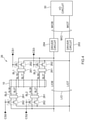
- a semiconductor device shown in FIG. 1 includes a memory cell array 10 , an access control circuit 20 that makes access to the memory cell array 10 , and an I/O circuit 30 that performs input and output of data.
- the memory cell array 10 includes a plurality of sub word lines SWL, a plurality of bit lines BL, and a plurality of memory cells MC arranged at respective intersections between the sub word lines SWL and the bit lines BL.
- the memory cells MC are, for example, DRAM cells.
- the access control circuit 20 includes a row address decoder 21 that decodes a row address XADD, a column address decoder 22 that decodes a column address YADD, and a command decoder 23 that decodes a command CMD.
- the row address decoder 21 predecodes the row address XADD supplied from outside, thereby generating a mat selection signal MAT, a main-word-line selection signal MW, and sub-word-line selection signals FXT and FXB.
- the access control circuit 20 further includes a main word driver 24 and a sub word driver 25 .
- the mat selection signal MAT and the main-word-line selection signal MW are supplied to the main word driver 24 .
- the main word driver 24 drives a main word signal MWLB based on the mat selection signal MAT and the main-word-line selection signal MW.
- the sub word driver 25 drives the sub word lines SWL based on the main word signal MWLB and the sub-word-line selection signals FXT and FXB.
- the column address decoder 22 decodes the column address YADD supplied from outside so as to generate a column selection signal CS.
- the column selection signal CS is supplied to a data sense circuit 26 included in the access control circuit 20 .
- the data sense circuit 26 is connected to the bit lines BL, and any of the bit lines BL which is indicated by the column selection signal CS is connected to the I/O circuit 30 .
- the command decoder 23 decodes the command CMD issued from outside so as to generate various internal control signals. For example, the command decoder 23 activates an active signal IACT in a case where the command CMD indicates an active command, activates a column enable signal CYE in a case where the command CMD indicates a read command or a write command, and activates a mode register read signal MRR in a case where the command CMU indicates a mode register read command.
- the active signal IACT is supplied to a timing control circuit 27 included in the access control circuit 20 .
- the timing control circuit 27 activates timing signals R 1 and R 2 in this order when the active signal IACT is activated.
- the timing signals R 1 and R 2 are supplied to the main word driver 24 .
- the column enable signal CYE is supplied to the column address decoder 22 .
- the column address decoder 22 activates the column selection signal CS in response to the column enable signal CYE.
- the activate signal TACT and the timing signals R 1 and R 2 may be considered as row-system signals, which are related to accessing a main or sub word line.
- the column enable signal CYE may be considered as a column-system signal, which is related to accessing hit lines BL.
- the mode register read signal MRR is supplied to a mode register 40 .
- the mode register 40 is a circuit that stores various operation parameters therein. When the mode register read signal MRR is activated, the parameters stored in the mode register 40 are output to outside via the I/O circuit 30 . The parameters stored in the mode register 40 can be overwritten from outside via the I/O circuit 30 .
- the semiconductor device further includes a signal monitor circuit 50 .
- the signal monitor circuit 50 is a circuit for evaluating activation timings of various internal signals of the semiconductor device.
- the active signal IACT, the timing signal R 2 , and the column enable signal CYE are input to the signal monitor circuit 50 .
- the signal monitor circuit 50 may evaluate the activation timings of various internal signals in parallel to an operation of the access control circuit 20 in a normal operation, or may evaluate the activation timings of various internal signals in a period of an initializing operation performed after power on.
- the signal monitor circuit 50 at a timing at which a power-on reset circuit 60 that monitors the level of a power-supply potential VDD generates a monitoring start signal SM.
- the power-on reset circuit 60 activates the monitoring start signal SM, for example, at a timing at which the level of the power-supply potential VDD has reached a sufficient level for making access to the memory cell array 10 .
- the main word driver 24 includes a logic circuit 241 that receives the timing signals R 1 and R 2 and the mat selection signal MAT, a selection circuit 242 that is pre-charged by an output signal 241 a of the logic circuit 241 and is discharged by an output signal 241 b of the logic circuit 241 and the main-word-line selection signal MW, and an output circuit 243 that latches an output of the selection circuit 242 and outputs the main word signal MWLB.
- a level shifter circuit 244 is inserted between the logic circuit 241 and the selection circuit 242 .
- the logic circuit 241 sets the output signal 241 a at a low level when the mat selection signal MAT is activated to a high level in a period in which both the timing signals R 1 and R 2 are at a high level, thereby turning on a P-channel MOS transistor P 10 included in the selection circuit 242 .
- a boosted potential VPP is supplied to a source of the transistor VPP, and thus when the transistor P 10 is turned on, an internal node f is pre-charged to the boosted potential VPP. Thereafter, when at least one of the timing signals R 1 and R 2 is changed to a low level, the transistor P 10 is set in an off-state.
- the sub word driver 25 is configured by a P-channel MOS transistor P 20 and N-channel MOS transistors N 21 and N 22 , where drains thereof are connected to the sub word line SWL.
- the sub-word-line selection signal FXT is supplied to a source of the transistor P 20
- a potential VKK is supplied to sources of the transistors N 21 and N 22 .
- the main word signal MWLB is supplied to gates of the transistors P 20 and N 21
- the sub-word-line selection signal FXB is supplied to a gate of the transistor N 22 .
- the sub-word-line selection signals FXT and FXB are signals having an amplitude of VSS to VPP and make transition in synchronization with the timing signal R 1 .
- the sub word line SWL is driven to the level VPP via the transistor P 20 . Accordingly, read data is read out from a memory cell MC connected to that sub word line SWL via a corresponding bit line BL.
- the sub word line SWL is deactivated to a level VKK by the transistor N 21 .
- the data sense circuit 26 includes sense amplifiers 261 connected to bit line pairs BL 0 , BL 1 , BL 2 , and BL 3 , . . . and column switches 262 respectively assigned to the sense amplifiers 261 .
- the bit line pair BL 0 includes complimentary bit lines BL 0 T and BL 0 B
- the bit line pair BL 1 includes complimentary bit lines BL 1 T and BL 1 B
- the bit line pair BL 2 includes complimentary bit lines BL 2 T and BL 2 B
- the bit line pair BL 3 includes complimentary bit lines BL 3 T and BL 3 B.
- the column selection signals CS corresponding thereto are supplied respectively to the column switches 262 . More specifically, column selection signals CS 0 , CS 1 , CS 2 , and CS 3 are supplied to the column switches 262 corresponding to the bit line pairs BL 0 , BL 1 , BL 2 , and BL 3 , respectively.
- the column selection signals CS assigned to the same local I/O line pair are exclusively activated.
- the local I/O line pair LIO is connected to the I/O circuit 30 via a main I/O line pair MIO.
- the main I/O line pair MIO includes complementary main I/O lines MIOT and MIOB.
- a read operation read data read out from the memory cell array 10 is transferred to the I/O circuit 30 via the local I/O line pair LIO and the main I/O line pair MIO.
- write operation write data supplied from outside is transferred to the local I/O line pair LIP via the 110 circuit 30 and the main I/O line pair MIO.
- a driver circuit 263 is provided between the main I/O line MIOT and the local I/O line LIOT, and a driver circuit 264 is provided between the main I/O line MIOB and the local 110 line LIOB.
- the driver circuits 263 and 264 have a function of driving the local I/O line pair LIO in a write operation.
- the signal monitor circuit 50 includes an oscillator circuit 501 that generates an oscillation signal OSC, a counter circuit 502 that performs a counting operation in synchronization with the oscillation signal OSC, a fuse circuit 503 that holds a threshold value TH in a nonvolatile manner, and a comparator circuit 504 that compares a count value CNT of the counter circuit 502 and the threshold value TH with each other.
- the threshold value TH is a binary data that indicates an upper limit value or a lower limit value of the count value CNT.
- the threshold value TH may represent an upper limit or a lower limit for a time period, and the count value CNT may represent a measured time period.
- the comparator circuit 504 activates an alert signal ALF when the count value CNT is larger than the threshold value TH. In a case where the threshold value TH indicates the lower limit value, the comparator circuit 504 activates the alert signal ALT when the count value CNT is smaller than the threshold value TH. That is, an alert signal may be generated when a measured time period is an aberrant value.
- the counter circuit 502 starts a counting operation that is synchronized with the oscillation signal USC in response to a start signal STR, and stops the counting operation in response to a stop signal SIP
- the start signal STR and the stop signal SIP are internal signals having a critical timing difference therebetween.
- the active signal IACT is the start signal SIR and the timing signal R 2 is the stop signal STP
- the counting operation of the counter circuit 502 is started.
- the counting operation of the counter circuit 502 is stopped when the timing signal R 2 is activated.
- the timing of activation of the timing signal R 2 is a time t 11 .
- the count value CNT of the counter circuit 502 is A and is sufficiently smaller than the threshold value TH.
- the count value CNT of the counter circuit 502 increases. For example, in a case Where the timing of activation of the timing signal R 2 is a time t 12 , the count value CNT increases to B (>A). In a case Where the timing of activation of the timing signal R 2 is a time t 13 , the count value CNT increases to C (>B). In the example shown in FIG.
- the threshold value TH is set to be the count value B or more and the count value C or less. Therefore, in a case where the timing signal R 2 is activated at the time t 13 , the comparator circuit 504 activates the alert signal ALT. Accordingly, in a case where the time from activation of the active signal IACT to activation of the main word signal MWLB becomes longer to exceed a time corresponding to the threshold value TH, the alert signal ALT is generated.
- the timing signal R 2 is assumed as the start signal STR and the column enable signal CYE is assumed as the stop signal STP, it is possible to evaluate a time from activation of the main word signal MWLB to a power on of the column switch 262 .
- the timing signal R 2 is activated at a time t 20 shown in FIG. 7 .
- the counting operation of the counter circuit 502 is stopped when the column enable signal CYE is activated.
- the timing of activation of the column enable signal CYE is a time t 23 .
- the count value CNT of the counter circuit 502 is D and is sufficiently larger than the threshold value TH.
- the count value CNT of the counter circuit 502 decreases. For example, in a case where the timing of activation of the column enable signal CYE is a time t 22 , the count value CNT decreases to E ( ⁇ D). In a case where the timing of activation of the column enable signal CYE is a time t 21 , the count value CNT decreases to F ( ⁇ E).
- the threshold value TH is set to be the count value E or more and the count value F or less.
- the comparator circuit 504 activates the alert signal ALT. Accordingly, in a case where the time from activation of the main word signal MWLB to a power on of the column switch 262 becomes shorter beyond a time corresponding to the threshold value TH, the alert signal AIX is generated.
- the alert signal ALT is stored in the mode register 40 . Therefore, the alert signal ALT can be read out o outside via the I/O circuit 30 by issuing a mode register read command from outside.
- evaluation using the signal monitor circuit 50 employs an internal signal generated in actual access. However, there is less necessity for frequently performing evaluation using the signal monitor circuit 50 , because the signal monitor circuit 50 detects age deterioration caused by long-time use. Therefore, as shown in FIG. 8 , it suffices that the signal monitor circuit 50 is activated at a timing when the power-on reset circuit 60 generates the monitoring start signal SM after power on. In the example shown in FIG. 8 , the power is on at a time t 30 , and the power-on reset circuit 60 activates the monitoring start signal SM at a time t 31 . The, signal monitor circuit 50 performs a judgement sequence shown in FIG. 6 or 7 in response to the monitoring start signal SM and stores the result in the mode register 40 .
- the command decoder 23 internally generates the active signal IACT or the column enable signal CYE, which is a pseudo signal, in response to the monitoring start signal SM, thereby generating various internal signals generated in actual use, such as the timing signals R 1 and R 2 , in a pseudo manner. Thereafter, when a mode register read command is issued from outside, the mode register read signal MRR is activated, and the alert signal ALT stored in the mode register 40 is output to outside via the I/O circuit 30 .
- the internal signal input to the signal monitor circuit 50 may be a signal used in actual access or a replica of the signal used in actual access.
- a timing signal generation circuit 271 that generates the timing signal R 2 and a replica circuit 272 that generates a replica signal R 2 pm having the same waveform as the timing signal R 2 are provided in the timing control circuit 27 , and the timing signal R 2 is used in actual access and the replica signal R 2 pm is used in evaluation using the signal monitor circuit 50 .
- the replica circuit 272 a process monitor circuit mounted in a semiconductor device in advance can be used. When the replica signal R 2 pm is input to the signal monitor circuit 50 in this manner, fallout of a transmission path for transmitting the timing signal R 2 does not increase.
Landscapes
- Engineering & Computer Science (AREA)
- Theoretical Computer Science (AREA)
- Quality & Reliability (AREA)
- Physics & Mathematics (AREA)
- General Engineering & Computer Science (AREA)
- General Physics & Mathematics (AREA)
- Microelectronics & Electronic Packaging (AREA)
- Computer Hardware Design (AREA)
- Computer Vision & Pattern Recognition (AREA)
- Dram (AREA)
- For Increasing The Reliability Of Semiconductor Memories (AREA)
Abstract
Description
- There is a case Where a semiconductor device such as a DRAM includes an evaluation circuit referred to as “process monitor”. Evaluation data generated by the process monitor is output to a tester in a manufacturing stage of the semiconductor device, and judgment is made based on the evaluation data whether an internal circuit is operated at designed timings. However, even in a case where the internal circuit is operated at designed timings in the manufacturing stage, operation timings may be deviated because of age deterioration of elements forming the internal circuit. When the age deterioration progresses, in some cases, an operation error suddenly occurs years after shipping.
-
FIG. 1 is a block diagram showing a configuration of a semiconductor device according to an embodiment of the present disclosure. -
FIG. 2 is a circuit diagram of a main word driver. -
FIG. 3 is a circuit diagram of a sub word driver. -
FIG. 4 is a circuit diagram of a data sense circuit. -
FIG. 5 is a circuit diagram of a signal monitor circuit according to an embodiment of the disclosure. -
FIGS. 6 and 7 are timing charts of operations of the signal monitor circuit according to an embodiment of the disclosure. -
FIG. 8 is a timing chart showing an example of activating the signal monitor circuit in a period of an initializing operation according to an embodiment of the disclosure. -
FIG. 9 is a block diagram showing an example in which a replica circuit is provided in a timing control circuit according to an embodiment of the disclosure. - Various embodiments of the present invention will be explained below in detail with reference to the accompanying drawings. The following detailed description refers to the accompanying drawings that show, by way of illustration, specific aspects and embodiments in which the present invention may be practiced. These embodiments are described in sufficient detail to enable those skilled in the art to practice the present invention. Other embodiments may be utilized, and structural, logical and electrical changes may be made without departing from the scope of the present invention. The various embodiments disclosed herein are not necessary mutually exclusive, as some disclosed embodiments can be combined with one or more other disclosed embodiments to form new embodiments.
- A semiconductor device shown in
FIG. 1 includes amemory cell array 10, anaccess control circuit 20 that makes access to thememory cell array 10, and an I/O circuit 30 that performs input and output of data. Thememory cell array 10 includes a plurality of sub word lines SWL, a plurality of bit lines BL, and a plurality of memory cells MC arranged at respective intersections between the sub word lines SWL and the bit lines BL. The memory cells MC are, for example, DRAM cells. Theaccess control circuit 20 includes arow address decoder 21 that decodes a row address XADD, acolumn address decoder 22 that decodes a column address YADD, and acommand decoder 23 that decodes a command CMD. - The
row address decoder 21 predecodes the row address XADD supplied from outside, thereby generating a mat selection signal MAT, a main-word-line selection signal MW, and sub-word-line selection signals FXT and FXB. Theaccess control circuit 20 further includes amain word driver 24 and asub word driver 25. The mat selection signal MAT and the main-word-line selection signal MW are supplied to themain word driver 24. Themain word driver 24 drives a main word signal MWLB based on the mat selection signal MAT and the main-word-line selection signal MW. Thesub word driver 25 drives the sub word lines SWL based on the main word signal MWLB and the sub-word-line selection signals FXT and FXB. - The
column address decoder 22 decodes the column address YADD supplied from outside so as to generate a column selection signal CS. The column selection signal CS is supplied to adata sense circuit 26 included in theaccess control circuit 20. Thedata sense circuit 26 is connected to the bit lines BL, and any of the bit lines BL which is indicated by the column selection signal CS is connected to the I/O circuit 30. - The
command decoder 23 decodes the command CMD issued from outside so as to generate various internal control signals. For example, thecommand decoder 23 activates an active signal IACT in a case where the command CMD indicates an active command, activates a column enable signal CYE in a case where the command CMD indicates a read command or a write command, and activates a mode register read signal MRR in a case where the command CMU indicates a mode register read command. The active signal IACT is supplied to atiming control circuit 27 included in theaccess control circuit 20. Thetiming control circuit 27 activates timing signals R1 and R2 in this order when the active signal IACT is activated. The timing signals R1 and R2 are supplied to themain word driver 24. The column enable signal CYE is supplied to thecolumn address decoder 22. Thecolumn address decoder 22 activates the column selection signal CS in response to the column enable signal CYE. The activate signal TACT and the timing signals R1 and R2 may be considered as row-system signals, which are related to accessing a main or sub word line. The column enable signal CYE may be considered as a column-system signal, which is related to accessing hit lines BL. The mode register read signal MRR is supplied to amode register 40. Themode register 40 is a circuit that stores various operation parameters therein. When the mode register read signal MRR is activated, the parameters stored in themode register 40 are output to outside via the I/O circuit 30. The parameters stored in themode register 40 can be overwritten from outside via the I/O circuit 30. - The semiconductor device according to the present embodiment further includes a
signal monitor circuit 50. Thesignal monitor circuit 50 is a circuit for evaluating activation timings of various internal signals of the semiconductor device. In the example shown inFIG. 1 , the active signal IACT, the timing signal R2, and the column enable signal CYE are input to thesignal monitor circuit 50. Thesignal monitor circuit 50 may evaluate the activation timings of various internal signals in parallel to an operation of theaccess control circuit 20 in a normal operation, or may evaluate the activation timings of various internal signals in a period of an initializing operation performed after power on. In the latter case, it suffices to activate thesignal monitor circuit 50 at a timing at which a power-onreset circuit 60 that monitors the level of a power-supply potential VDD generates a monitoring start signal SM. The power-onreset circuit 60 activates the monitoring start signal SM, for example, at a timing at which the level of the power-supply potential VDD has reached a sufficient level for making access to thememory cell array 10. - As shown in
FIG. 2 , themain word driver 24 includes alogic circuit 241 that receives the timing signals R1 and R2 and the mat selection signal MAT, aselection circuit 242 that is pre-charged by anoutput signal 241 a of thelogic circuit 241 and is discharged by anoutput signal 241 b of thelogic circuit 241 and the main-word-line selection signal MW, and anoutput circuit 243 that latches an output of theselection circuit 242 and outputs the main word signal MWLB. Alevel shifter circuit 244 is inserted between thelogic circuit 241 and theselection circuit 242. - The
logic circuit 241 sets theoutput signal 241 a at a low level when the mat selection signal MAT is activated to a high level in a period in which both the timing signals R1 and R2 are at a high level, thereby turning on a P-channel MOS transistor P10 included in theselection circuit 242. A boosted potential VPP is supplied to a source of the transistor VPP, and thus when the transistor P10 is turned on, an internal node f is pre-charged to the boosted potential VPP. Thereafter, when at least one of the timing signals R1 and R2 is changed to a low level, the transistor P10 is set in an off-state. In this state, when the main-word-line selection signal MW becomes a high level and both the timing signals R1 and R2 are changed to be a low level, N-channel MOS transistors N11 and N12 both included in the selection circuit 42 are turned on. Therefore, the internal node f is discharged to a level VSS. As a result, the main word signal MWLB output from theoutput circuit 243 is activated to a potential VSS. On the other hand, when the main-word-line selection signal MW remains at a low level, the internal node f is maintained at a level VPP, and thus the main word signal MWLB remains in a deactivated state at the boosted potential VPP. - As shown in
FIG. 3 , thesub word driver 25 is configured by a P-channel MOS transistor P20 and N-channel MOS transistors N21 and N22, where drains thereof are connected to the sub word line SWL. The sub-word-line selection signal FXT is supplied to a source of the transistor P20, and a potential VKK is supplied to sources of the transistors N21 and N22. Further, the main word signal MWLB is supplied to gates of the transistors P20 and N21, and the sub-word-line selection signal FXB is supplied to a gate of the transistor N22. The sub-word-line selection signals FXT and FXB are signals having an amplitude of VSS to VPP and make transition in synchronization with the timing signal R1. - With this configuration, when the main word signal MWLB is activated to a low level (a level VSS) while the sub-word-line selection signals FXT and FXB are at a level VPP and the level VSS, respectively, the sub word line SWL is driven to the level VPP via the transistor P20. Accordingly, read data is read out from a memory cell MC connected to that sub word line SWL via a corresponding bit line BL. On the other hand, in a case where the main word signal MWLB is deactivated at a high level (the level VPP) even while the sub-word-line selection signals FXB and FXB are at the level VPP and the level VSS, respectively, the sub word line SWL is deactivated to a level VKK by the transistor N21.
- As shown in
FIG. 4 , thedata sense circuit 26 includessense amplifiers 261 connected to bit line pairs BL0, BL1, BL2, and BL3, . . . and column switches 262 respectively assigned to thesense amplifiers 261. The bit line pair BL0 includes complimentary bit lines BL0T and BL0B, the bit line pair BL1 includes complimentary bit lines BL1T and BL1B, the bit line pair BL2 includes complimentary bit lines BL2T and BL2B, and the bit line pair BL3 includes complimentary bit lines BL3T and BL3B. The bit line pairs BL0, BL1, BL2, and BL3, . . . are respectively connected to a local I/O line pair LIO via a corresponding one of thesense amplifiers 261 and a corresponding one of the column switches 262. The column selection signals CS corresponding thereto are supplied respectively to the column switches 262. More specifically, column selection signals CS0, CS1, CS2, and CS3 are supplied to the column switches 262 corresponding to the bit line pairs BL0, BL1, BL2, and BL3, respectively. The column selection signals CS assigned to the same local I/O line pair are exclusively activated. - The local I/O line pair LIO is connected to the I/
O circuit 30 via a main I/O line pair MIO. The main I/O line pair MIO includes complementary main I/O lines MIOT and MIOB. In a read operation, read data read out from thememory cell array 10 is transferred to the I/O circuit 30 via the local I/O line pair LIO and the main I/O line pair MIO. In a write operation, write data supplied from outside is transferred to the local I/O line pair LIP via the 110circuit 30 and the main I/O line pair MIO. Adriver circuit 263 is provided between the main I/O line MIOT and the local I/O line LIOT, and adriver circuit 264 is provided between the main I/O line MIOB and the local 110 line LIOB. Thedriver circuits - As shown in
FIG. 5 , thesignal monitor circuit 50 includes anoscillator circuit 501 that generates an oscillation signal OSC, acounter circuit 502 that performs a counting operation in synchronization with the oscillation signal OSC, afuse circuit 503 that holds a threshold value TH in a nonvolatile manner, and acomparator circuit 504 that compares a count value CNT of thecounter circuit 502 and the threshold value TH with each other. The threshold value TH is a binary data that indicates an upper limit value or a lower limit value of the count value CNT. The threshold value TH may represent an upper limit or a lower limit for a time period, and the count value CNT may represent a measured time period. In a case where the threshold value indicates the upper limit value, thecomparator circuit 504 activates an alert signal ALF when the count value CNT is larger than the threshold value TH. In a case where the threshold value TH indicates the lower limit value, thecomparator circuit 504 activates the alert signal ALT when the count value CNT is smaller than the threshold value TH. That is, an alert signal may be generated when a measured time period is an aberrant value. - The
counter circuit 502 starts a counting operation that is synchronized with the oscillation signal USC in response to a start signal STR, and stops the counting operation in response to a stop signal SIP The start signal STR and the stop signal SIP are internal signals having a critical timing difference therebetween. For example, assuming that the active signal IACT is the start signal SIR and the timing signal R2 is the stop signal STP, it is possible to evaluate a time from activation of the active signal IACT to activation of the main word signal MWLB. In this case, when the active signal IACT is activated at a time t10 shown inFIG. 6 , the counting operation of thecounter circuit 502 is started. The counting operation of thecounter circuit 502 is stopped when the timing signal R2 is activated. In an initial state after manufacturing, the timing of activation of the timing signal R2 is a time t11. In this case, the count value CNT of thecounter circuit 502 is A and is sufficiently smaller than the threshold value TH. However, When the timing of activation of the timing signal R2 is delayed because of age deterioration of elements, the count value CNT of thecounter circuit 502 increases. For example, in a case Where the timing of activation of the timing signal R2 is a time t12, the count value CNT increases to B (>A). In a case Where the timing of activation of the timing signal R2 is a time t13, the count value CNT increases to C (>B). In the example shown inFIG. 6 , the threshold value TH is set to be the count value B or more and the count value C or less. Therefore, in a case where the timing signal R2 is activated at the time t13, thecomparator circuit 504 activates the alert signal ALT. Accordingly, in a case where the time from activation of the active signal IACT to activation of the main word signal MWLB becomes longer to exceed a time corresponding to the threshold value TH, the alert signal ALT is generated. - Alternatively, when the timing signal R2 is assumed as the start signal STR and the column enable signal CYE is assumed as the stop signal STP, it is possible to evaluate a time from activation of the main word signal MWLB to a power on of the
column switch 262. In this case, when the timing signal R2 is activated at a time t20 shown inFIG. 7 , a counting operation of thecounter circuit 502 is started. The counting operation of thecounter circuit 502 is stopped when the column enable signal CYE is activated. In an initial state after manufacturing, the timing of activation of the column enable signal CYE is a time t23. In this case, the count value CNT of thecounter circuit 502 is D and is sufficiently larger than the threshold value TH. However, when the timing of activation of the column enable signal CYE is advanced (or the timing of activation of the timing signal R2 is delayed) because of age deterioration of elements, the count value CNT of thecounter circuit 502 decreases. For example, in a case where the timing of activation of the column enable signal CYE is a time t22, the count value CNT decreases to E (<D). In a case where the timing of activation of the column enable signal CYE is a time t21, the count value CNT decreases to F (<E). In the example shown inFIG. 7 , the threshold value TH is set to be the count value E or more and the count value F or less. Therefore, in a case where the column enable signal CYE is activated at the time t21, thecomparator circuit 504 activates the alert signal ALT. Accordingly, in a case where the time from activation of the main word signal MWLB to a power on of thecolumn switch 262 becomes shorter beyond a time corresponding to the threshold value TH, the alert signal AIX is generated. - The alert signal ALT is stored in the
mode register 40. Therefore, the alert signal ALT can be read out o outside via the I/O circuit 30 by issuing a mode register read command from outside. - It is possible that evaluation using the
signal monitor circuit 50 employs an internal signal generated in actual access. However, there is less necessity for frequently performing evaluation using thesignal monitor circuit 50, because thesignal monitor circuit 50 detects age deterioration caused by long-time use. Therefore, as shown inFIG. 8 , it suffices that thesignal monitor circuit 50 is activated at a timing when the power-onreset circuit 60 generates the monitoring start signal SM after power on. In the example shown inFIG. 8 , the power is on at a time t30, and the power-onreset circuit 60 activates the monitoring start signal SM at a time t31. The,signal monitor circuit 50 performs a judgement sequence shown inFIG. 6 or 7 in response to the monitoring start signal SM and stores the result in themode register 40. In this case, thecommand decoder 23 internally generates the active signal IACT or the column enable signal CYE, which is a pseudo signal, in response to the monitoring start signal SM, thereby generating various internal signals generated in actual use, such as the timing signals R1 and R2, in a pseudo manner. Thereafter, when a mode register read command is issued from outside, the mode register read signal MRR is activated, and the alert signal ALT stored in themode register 40 is output to outside via the I/O circuit 30. - The internal signal input to the
signal monitor circuit 50 may be a signal used in actual access or a replica of the signal used in actual access. For example, as shown inFIG. 9 , it is possible to configure that a timingsignal generation circuit 271 that generates the timing signal R2 and areplica circuit 272 that generates a replica signal R2 pm having the same waveform as the timing signal R2 are provided in thetiming control circuit 27, and the timing signal R2 is used in actual access and the replica signal R2 pm is used in evaluation using thesignal monitor circuit 50. As thereplica circuit 272, a process monitor circuit mounted in a semiconductor device in advance can be used. When the replica signal R2 pm is input to thesignal monitor circuit 50 in this manner, fallout of a transmission path for transmitting the timing signal R2 does not increase. - Although this invention has been disclosed in the context of certain preferred embodiments and examples, it will be understood by those skilled in the art that the inventions extend beyond the specifically disclosed embodiments to other alternative embodiments and/or uses of the inventions and obvious modifications and equivalents thereof. In addition, other modifications which are within the scope of this invention will be readily apparent to those of skill in the art based on this disclosure. It is also contemplated that various combination or sub-combination of the specific features and aspects of the embodiments may be made and still fall within the scope of the inventions. It should be understood that various features and aspects of the disclosed embodiments can be combined with or substituted for one another in order to form varying mode of the disclosed invention. Thus, it is intended that the scope of at least some of the present invention herein disclosed should not be limited by the particular disclosed embodiments described above.
Claims (20)
Priority Applications (2)
| Application Number | Priority Date | Filing Date | Title |
|---|---|---|---|
| US16/992,007 US11567820B2 (en) | 2020-08-12 | 2020-08-12 | Internal signal monitoring circuit |
| CN202110919141.3A CN114078514A (en) | 2020-08-12 | 2021-08-11 | Internal signal monitoring circuit |
Applications Claiming Priority (1)
| Application Number | Priority Date | Filing Date | Title |
|---|---|---|---|
| US16/992,007 US11567820B2 (en) | 2020-08-12 | 2020-08-12 | Internal signal monitoring circuit |
Publications (2)
| Publication Number | Publication Date |
|---|---|
| US20220050737A1 true US20220050737A1 (en) | 2022-02-17 |
| US11567820B2 US11567820B2 (en) | 2023-01-31 |
Family
ID=80224265
Family Applications (1)
| Application Number | Title | Priority Date | Filing Date |
|---|---|---|---|
| US16/992,007 Active 2041-04-09 US11567820B2 (en) | 2020-08-12 | 2020-08-12 | Internal signal monitoring circuit |
Country Status (2)
| Country | Link |
|---|---|
| US (1) | US11567820B2 (en) |
| CN (1) | CN114078514A (en) |
Cited By (2)
| Publication number | Priority date | Publication date | Assignee | Title |
|---|---|---|---|---|
| CN114727051A (en) * | 2022-06-06 | 2022-07-08 | 宏晶微电子科技股份有限公司 | Media resource transmission device, system and method |
| US11418195B1 (en) * | 2020-07-15 | 2022-08-16 | Marvell Asia Pte, Ltd. | Voltage power switch |
Citations (3)
| Publication number | Priority date | Publication date | Assignee | Title |
|---|---|---|---|---|
| US20060274875A1 (en) * | 2005-06-06 | 2006-12-07 | Vereen Jerry D | Interface circuit for a media access controller and an optical line termination transceiver module |
| US20070116169A1 (en) * | 2003-12-18 | 2007-05-24 | Michel Robbe | Phase-locked loop |
| US20090092000A1 (en) * | 2007-08-10 | 2009-04-09 | Fujitsu Limited | Semiconductor memory device with reduced current consumption |
Family Cites Families (2)
| Publication number | Priority date | Publication date | Assignee | Title |
|---|---|---|---|---|
| KR102410566B1 (en) * | 2018-02-05 | 2022-06-17 | 삼성전자주식회사 | Semiconductor memory devices, memory systems including the same and method of operating semiconductor memory devices |
| US10559370B2 (en) * | 2018-03-22 | 2020-02-11 | Sandisk Technologies Llc | System and method for in-situ programming and read operation adjustments in a non-volatile memory |
-
2020
- 2020-08-12 US US16/992,007 patent/US11567820B2/en active Active
-
2021
- 2021-08-11 CN CN202110919141.3A patent/CN114078514A/en active Pending
Patent Citations (3)
| Publication number | Priority date | Publication date | Assignee | Title |
|---|---|---|---|---|
| US20070116169A1 (en) * | 2003-12-18 | 2007-05-24 | Michel Robbe | Phase-locked loop |
| US20060274875A1 (en) * | 2005-06-06 | 2006-12-07 | Vereen Jerry D | Interface circuit for a media access controller and an optical line termination transceiver module |
| US20090092000A1 (en) * | 2007-08-10 | 2009-04-09 | Fujitsu Limited | Semiconductor memory device with reduced current consumption |
Cited By (3)
| Publication number | Priority date | Publication date | Assignee | Title |
|---|---|---|---|---|
| US11418195B1 (en) * | 2020-07-15 | 2022-08-16 | Marvell Asia Pte, Ltd. | Voltage power switch |
| US11742858B1 (en) | 2020-07-15 | 2023-08-29 | Marvell Asia Pte, Ltd. | Voltage power switch |
| CN114727051A (en) * | 2022-06-06 | 2022-07-08 | 宏晶微电子科技股份有限公司 | Media resource transmission device, system and method |
Also Published As
| Publication number | Publication date |
|---|---|
| US11567820B2 (en) | 2023-01-31 |
| CN114078514A (en) | 2022-02-22 |
Similar Documents
| Publication | Publication Date | Title |
|---|---|---|
| KR102634234B1 (en) | Apparatus and method for soft post/package recovery | |
| US6424142B1 (en) | Semiconductor device operable in a plurality of test operation modes | |
| US20190267077A1 (en) | Semiconductor device | |
| US6205067B1 (en) | Semiconductor memory device having burn-in mode operation stably accelerated | |
| US8488380B2 (en) | Word line driving circuit, semiconductor memory device including the same, and method for testing the semiconductor memory device | |
| US6522567B2 (en) | Semiconductor memory device and semiconductor integrated device using the same | |
| US8923082B2 (en) | Semiconductor device on which wafer-level burn-in test is performed and manufacturing method thereof | |
| US20040196719A1 (en) | Semiconductor memory device having reduced current dissipation in data holding mode | |
| US6728149B2 (en) | Semiconductor memory device | |
| US11567820B2 (en) | Internal signal monitoring circuit | |
| US6349064B1 (en) | Semiconductor memory device capable of independent selection of normal and redundant memory cells after programming of redundant address | |
| JPH1139862A (en) | Semiconductor storage device | |
| US6894942B2 (en) | Refresh control circuit and method for semiconductor memory device | |
| US6535438B2 (en) | Semiconductor memory device adopting redundancy system | |
| US6233183B1 (en) | Semiconductor memory device with high data access speed | |
| US11069384B2 (en) | Apparatuses and methods for compensation of sense amplifiers | |
| US10068662B2 (en) | Semiconductor device including a roll call circuit for outputting addresses of defective memory cells | |
| US20030048680A1 (en) | Semiconductor memory device having a plurality of signal lines for writing and reading data | |
| US7075854B2 (en) | Semiconductor memory device, write control circuit and write control method for the same | |
| US8463572B2 (en) | Semiconductor device | |
| US6628559B2 (en) | Semiconductor memory device having refreshing function | |
| US6519193B2 (en) | Semiconductor integrated circuit device having spare word lines | |
| US7366037B2 (en) | Semiconductor memory | |
| KR100397901B1 (en) | Semiconductor storage device | |
| US20230207034A1 (en) | Semiconductor device and testing method for memory circuit |
Legal Events
| Date | Code | Title | Description |
|---|---|---|---|
| AS | Assignment |
Owner name: MICRON TECHNOLOGY, INC., IDAHO Free format text: ASSIGNMENT OF ASSIGNORS INTEREST;ASSIGNOR:SAKAMOTO, YUSUKE;REEL/FRAME:053479/0497 Effective date: 20200812 |
|
| FEPP | Fee payment procedure |
Free format text: ENTITY STATUS SET TO UNDISCOUNTED (ORIGINAL EVENT CODE: BIG.); ENTITY STATUS OF PATENT OWNER: LARGE ENTITY |
|
| STPP | Information on status: patent application and granting procedure in general |
Free format text: NON FINAL ACTION MAILED |
|
| STPP | Information on status: patent application and granting procedure in general |
Free format text: NON FINAL ACTION MAILED |
|
| STPP | Information on status: patent application and granting procedure in general |
Free format text: RESPONSE TO NON-FINAL OFFICE ACTION ENTERED AND FORWARDED TO EXAMINER |
|
| STPP | Information on status: patent application and granting procedure in general |
Free format text: NOTICE OF ALLOWANCE MAILED -- APPLICATION RECEIVED IN OFFICE OF PUBLICATIONS |
|
| STPP | Information on status: patent application and granting procedure in general |
Free format text: PUBLICATIONS -- ISSUE FEE PAYMENT VERIFIED |
|
| STCF | Information on status: patent grant |
Free format text: PATENTED CASE |