US20210375813A1 - Mechanical punched via formation in electronics package and electronics package formed thereby - Google Patents
Mechanical punched via formation in electronics package and electronics package formed thereby Download PDFInfo
- Publication number
- US20210375813A1 US20210375813A1 US15/929,925 US202015929925A US2021375813A1 US 20210375813 A1 US20210375813 A1 US 20210375813A1 US 202015929925 A US202015929925 A US 202015929925A US 2021375813 A1 US2021375813 A1 US 2021375813A1
- Authority
- US
- United States
- Prior art keywords
- insulating substrate
- electrically insulating
- vias
- adhesive layer
- electronics package
- Prior art date
- Legal status (The legal status is an assumption and is not a legal conclusion. Google has not performed a legal analysis and makes no representation as to the accuracy of the status listed.)
- Granted
Links
Images


Classifications
-
- H01L24/19—
-
- H—ELECTRICITY
- H10—SEMICONDUCTOR DEVICES; ELECTRIC SOLID-STATE DEVICES NOT OTHERWISE PROVIDED FOR
- H10W—GENERIC PACKAGES, INTERCONNECTIONS, CONNECTORS OR OTHER CONSTRUCTIONAL DETAILS OF DEVICES COVERED BY CLASS H10
- H10W70/00—Package substrates; Interposers; Redistribution layers [RDL]
- H10W70/01—Manufacture or treatment
- H10W70/05—Manufacture or treatment of insulating or insulated package substrates, or of interposers, or of redistribution layers
- H10W70/095—Manufacture or treatment of insulating or insulated package substrates, or of interposers, or of redistribution layers of vias therein
-
- H01L24/20—
-
- H—ELECTRICITY
- H10—SEMICONDUCTOR DEVICES; ELECTRIC SOLID-STATE DEVICES NOT OTHERWISE PROVIDED FOR
- H10W—GENERIC PACKAGES, INTERCONNECTIONS, CONNECTORS OR OTHER CONSTRUCTIONAL DETAILS OF DEVICES COVERED BY CLASS H10
- H10W70/00—Package substrates; Interposers; Redistribution layers [RDL]
- H10W70/60—Insulating or insulated package substrates; Interposers; Redistribution layers
-
- H—ELECTRICITY
- H10—SEMICONDUCTOR DEVICES; ELECTRIC SOLID-STATE DEVICES NOT OTHERWISE PROVIDED FOR
- H10W—GENERIC PACKAGES, INTERCONNECTIONS, CONNECTORS OR OTHER CONSTRUCTIONAL DETAILS OF DEVICES COVERED BY CLASS H10
- H10W70/00—Package substrates; Interposers; Redistribution layers [RDL]
- H10W70/01—Manufacture or treatment
- H10W70/05—Manufacture or treatment of insulating or insulated package substrates, or of interposers, or of redistribution layers
- H10W70/08—Manufacture or treatment of insulating or insulated package substrates, or of interposers, or of redistribution layers by depositing layers on the chip or wafer, e.g. "chip-first" RDLs
- H10W70/09—Manufacture or treatment of insulating or insulated package substrates, or of interposers, or of redistribution layers by depositing layers on the chip or wafer, e.g. "chip-first" RDLs extending onto an encapsulation that laterally surrounds the chip or wafer, e.g. fan-out wafer level package [FOWLP] RDLs
-
- H—ELECTRICITY
- H10—SEMICONDUCTOR DEVICES; ELECTRIC SOLID-STATE DEVICES NOT OTHERWISE PROVIDED FOR
- H10W—GENERIC PACKAGES, INTERCONNECTIONS, CONNECTORS OR OTHER CONSTRUCTIONAL DETAILS OF DEVICES COVERED BY CLASS H10
- H10W70/00—Package substrates; Interposers; Redistribution layers [RDL]
- H10W70/01—Manufacture or treatment
- H10W70/05—Manufacture or treatment of insulating or insulated package substrates, or of interposers, or of redistribution layers
- H10W70/093—Connecting or disconnecting other interconnections thereto or therefrom, e.g. connecting bond wires or bumps
-
- H—ELECTRICITY
- H10—SEMICONDUCTOR DEVICES; ELECTRIC SOLID-STATE DEVICES NOT OTHERWISE PROVIDED FOR
- H10W—GENERIC PACKAGES, INTERCONNECTIONS, CONNECTORS OR OTHER CONSTRUCTIONAL DETAILS OF DEVICES COVERED BY CLASS H10
- H10W70/00—Package substrates; Interposers; Redistribution layers [RDL]
- H10W70/60—Insulating or insulated package substrates; Interposers; Redistribution layers
- H10W70/62—Insulating or insulated package substrates; Interposers; Redistribution layers characterised by their interconnections
- H10W70/65—Shapes or dispositions of interconnections
- H10W70/652—Cross-sectional shapes
- H10W70/6528—Cross-sectional shapes of the portions that connect to chips, wafers or package parts
-
- H—ELECTRICITY
- H10—SEMICONDUCTOR DEVICES; ELECTRIC SOLID-STATE DEVICES NOT OTHERWISE PROVIDED FOR
- H10W—GENERIC PACKAGES, INTERCONNECTIONS, CONNECTORS OR OTHER CONSTRUCTIONAL DETAILS OF DEVICES COVERED BY CLASS H10
- H10W72/00—Interconnections or connectors in packages
- H10W72/01—Manufacture or treatment
- H10W72/0198—Manufacture or treatment batch processes
-
- H—ELECTRICITY
- H10—SEMICONDUCTOR DEVICES; ELECTRIC SOLID-STATE DEVICES NOT OTHERWISE PROVIDED FOR
- H10W—GENERIC PACKAGES, INTERCONNECTIONS, CONNECTORS OR OTHER CONSTRUCTIONAL DETAILS OF DEVICES COVERED BY CLASS H10
- H10W72/00—Interconnections or connectors in packages
- H10W72/071—Connecting or disconnecting
- H10W72/073—Connecting or disconnecting of die-attach connectors
Definitions
- Embodiments of the invention relate generally to structures and methods for packaging semiconductor devices and, more particularly, to a power electronics package structure having vias formed by a mechanical punching operation, with the vias providing for formation of metal interconnects down to a power device, such as by a power overlay (POL) interconnect formation process.
- POL power overlay
- Electronics packaging is a method for constructing electronic circuits packages or modules in which one or more semiconductor devices and/or passive devices are incorporated within a package structure that provides electrical connections and protection to the devices—such that a “multi-chip module” (MCM) might be provided, for example.
- MCM multi-chip module
- the package structure then enables connection of the package/module to the surface of printed circuit boards (PCBs) or other similar external circuits, for example.
- PCBs printed circuit boards
- An example of one such electronics package structure is a power electronics package structure or module formed using a POL process.
- the technique for packaging semiconductor devices and passive devices using a POL process typically begins with placement of one or more semiconductor or passive devices onto a dielectric layer by way of an adhesive, with the dielectric layer covering the active side of each device. Vias are formed through the dielectric layer and adhesive—either prior or subsequent to attachment of the device(s)—and metal interconnects are then electroplated onto the dielectric layer and in/through the vias (i.e., metallized vias) to form a direct metallic connection to the device(s).
- the metal interconnects may be formed as thicker POL interconnects.
- the interconnects may be routed through additional laminate re-distribution layers, if desired, and an input/output system is provided to enable surface mounting of the package onto the PCB or external circuit.
- An embedding compound may then be applied about the device(s) to encapsulate the device(s) therein.
- vias in the package structure may be performed according to any of a number of known techniques and, in embodiments where vias are formed prior to attachment of an electronic component, vias may be formed only through a dielectric layer or formed through both a dielectric layer and an adhesive layer applied thereto. In embodiments where vias are formed through just the dielectric layer, such as when making a double-sided flex circuit, the vias may be formed by processes such as laser drilling or ablation, plasma etching, wet etching, water jetting, photo-definition, mechanical punching, or mechanical drilling.
- the vias may be formed by processes such as laser drilling or ablation, plasma etching, wet etching, water jetting, or photo-definition, but mechanical punching and/or mechanical drilling is avoided due to issues with adhesive building-up on the mechanical punching/drilling tool. Also, regarding via formation using mechanical punching, it is recognized that mechanical punching is limited to “larger” via diameters and pitches.
- an electronics package includes an electrically insulating substrate having a first surface and a second surface, an adhesive layer positioned on the first surface of the electrically insulating substrate, and an electrical component having a top surface coupled to the adhesive layer on a surface thereof opposite the electrically insulating substrate, the electrical component having one or more contact pads on the top surface.
- One or more vias are formed through the electrically insulating substrate and the adhesive layer at locations corresponding to respective ones of the one or more contact pads, each of the one or more vias having a via wall extending from the second surface of the electrically insulating substrate to a respective contact pad.
- the electrically insulating substrate comprises a protrusion extending outwardly from the first surface thereof so as to cover at least part of the adhesive layer in forming part of the via wall.
- a method for manufacturing an electronics package includes providing an electrically insulating substrate, applying or forming an adhesive layer on a first surface of the electrically insulating substrate, and forming one or more vias through the electrically insulating substrate and the adhesive layer, each of the one or more vias defined by a via wall.
- the one or more vias are formed by mechanically punching the one or more vias through the electrically insulating substrate and the adhesive layer using a mechanical punching tool, with the one or more vias being mechanically punched through the electrically insulating substrate and the adhesive layer from a second surface side of the electrically insulating substrate, through the electrically insulating substrate and then through the adhesive layer.
- an electronics package is provided that is formed by a process including providing an electrically insulating substrate having a first surface and a second surface, applying or forming an adhesive layer on the first surface of the electrically insulating substrate, and forming one or more vias through the electrically insulating substrate and the adhesive layer by mechanically punching the one or more vias through the electrically insulating substrate and the adhesive layer using a mechanical punching tool positioned on the second surface side of the electrically insulating substrate, each of the one or more vias defined by a via wall.
- the mechanical punching of the one or more vias through the electrically insulating substrate and the adhesive layer from the second surface side of the electrically insulating substrate forms a protrusion on the electrically insulating substrate at each via that extends outwardly from the first surface, so as to cover at least part of the adhesive layer and form part of the via wall.
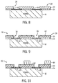
- FIG. 1 is a schematic cross-sectional side view of an electronics package, according to an embodiment of the invention.
- FIG. 2 is a detailed view of a portion of the electronics package of FIG. 1 .
- FIGS. 3-15 are schematic cross-sectional side views of the electronics package of FIG. 1 during various stages of a manufacturing/build-up process, according to an embodiment of the invention.
- FIG. 16 is a schematic cross-sectional view of an electronics package, according to another embodiment of the invention.
- FIG. 17 is a schematic cross-sectional side view of an electronics package, where laser drilling is performed subsequent to a mechanical punching operation, according to an embodiment of the invention.
- Embodiments of the present invention provide for an electronics package structure having vias formed by a mechanical punching operation.
- the electronics package includes an electrically insulating substrate and adhesive layer having vias formed therethrough each defined by a via wall, wherein at each via the electrically insulating substrate includes a protrusion extending outwardly from a surface thereof, around a perimeter of the via, so as to cover at least part of the adhesive layer in forming part of the via wall.
- electrical component may be understood to encompass any of the various types of semiconductor devices described above as well as resistors, capacitors, inductors, filters, and other circuit devices, and it is to be understood that mechanically punched vias, as described in greater detail here below, can be used to interconnect to any of these devices.
- Electrical component 12 may be a power semiconductor component or chip 12 (and is described hereafter as such) that has an active surface 14 with at least one contact pad or I/O pad 16 , 18 thereon.
- the active surface 14 of power semiconductor chip 12 is coupled to the first surface 20 of an electrically insulating substrate 22 or support substrate by way of an adhesive layer 24 .
- insulating substrate 22 may be provided in the form of an insulating film or dielectric substrate, such as for example a Kapton® laminate flex, an organic film or substrate comprising polyimide, epoxy, BT resin, although other suitable materials may also be employed, such as Ultem®, polytetrafluoroethylene (PTFE), or another polymer film, such as a liquid crystal polymer (LCP) or a polyimide substrate, or inorganic substrates such as Si, SiC, AN, ceramic, or glass, as non-limiting examples.
- a Kapton® laminate flex an organic film or substrate comprising polyimide, epoxy, BT resin, although other suitable materials may also be employed, such as Ultem®, polytetrafluoroethylene (PTFE), or another polymer film, such as a liquid crystal polymer (LCP) or a polyimide substrate, or inorganic substrates such as Si, SiC, AN, ceramic, or glass, as non-limiting examples.
- the adhesive layer 24 is composed of a bonding material that is preferably a non-electrically conducting polymeric material (e.g., epoxy, liquid crystal polymer, ceramic or metal filled polymers) or other organic material as non-limiting examples.
- a bonding material e.g., epoxy, liquid crystal polymer, ceramic or metal filled polymers
- suitable bonding materials include ePDA or other Henkel adhesives, for example.
- At least one via 26 extends between the first surface 20 and second surface 28 of insulating substrate 22 and through adhesive layer 24 , with two vias illustrated in FIG. 1 —each of the vias 26 defined by a via wall 30 .
- Vias 26 are aligned with the I/O pad(s) 16 , 18 of the power semiconductor chip 12 .
- An electrically conductive first interconnect layer 32 or power interconnect layer is disposed on a portion of the second surface 28 of insulating substrate 22 .
- the first interconnect layer 32 extends into the vias 26 , forming conductive vias 34 , and also extends onto the I/O pad(s) 16 , 18 of power semiconductor chip 12 .
- power semiconductor chip 12 includes two I/O pads 16 , 18 on active surface 14 .
- I/O pad 16 is a gate pad and covers a smaller area than I/O pad 18 , which could be a source pad.
- a via 26 formed down to a gate I/O pad 16 may have a diameter of 300 micrometers, while a via 26 formed down to a source I/O pad 18 may have a diameter of 500 micrometers.
- power semiconductor chip 12 is illustrated in FIG. 1 as including two I/O pads 16 , 18 , it may have three or more I/O pads in some alternative embodiments or may include only one topside I/O pad in another alternative embodiment, such as where element 12 is a power diode for example.
- electrical component 12 is provided as a logic semiconductor chip, the chip may have as few as four I/O pads or may have more than ten, hundreds, or thousands of I/O pads.
- electrical component 12 is provided as a resistor, capacitor, or feed thru shim, for example, that may have one contact pad or multiple contact pads.
- First interconnect layer 32 is an electrically conductive material and, preferably, is composed of one or more metals such as aluminum, copper, gold, silver, nickel, or combinations thereof as non-limiting examples, i.e., metallized vias.
- first interconnect layer 32 may be an electrically conductive polymer or formed using inks that contain conductive metal particles.
- First interconnect layer 32 may be composed of a barrier or adhesion layer, a seed layer, and a relatively thick layer of bulk material that is plated atop the seed and barrier layers achieving the desired conductive layer thickness.
- the barrier layer and/or the seed layer may be omitted from first interconnect layer 32 .
- the barrier layer when used, is applied to the insulating substrate 22 prior to application of the seed layer and bulk material.
- the barrier layer may include titanium or chromium, as non-limiting examples.
- seed metal layer may be an electrically conductive material such as copper, as one non-limiting example.
- the layer of bulk material is plated up to achieve the desired thickness of first interconnect layer 32 .
- the bulk material portion of first interconnect layer 32 includes at least one electrically conductive material such as copper, aluminum, or other standard wiring material.
- the barrier layer may have a thickness in the approximate range of 0.1 to 0.4 microns
- the seed metal layer may have a thickness in the approximate range of 1 to 3 microns
- the bulk layer may have a thickness in the approximate range of 10 to 100 microns.
- other materials at other thicknesses can be used to form first interconnect layer 32 based on design requirements.
- a solder mask layer or other insulating material 36 may be applied over the exposed top surfaces of the first interconnect layer 32 and the insulating layer 22 to provide a protective coating and define a location for interconnect pads.
- a capping layer 38 can then be applied to the top surface of these interconnect pads, such as Eless Ni/Au or ENIPG, to provide a solderable wirebondable finish.
- a series of input/output (I/O) connections 40 would then be formed to provide a route for electrical connections between the power semiconductor chip 12 and external components (not shown) such as, for example a busbar or printed circuit board (PCB).
- I/O connections may be provided in the form of plated bumps or pillar bumps, as non-limiting examples.
- a DBC substrate can be attached to the back side of the power semiconductor chip 12 .
- An encapsulant or insulating material may then be used to underfill between the insulating substrate 22 and the DBC substrate.
- additional insulating layers and interconnect layers e.g., a second insulating layer and second interconnect layer, could be provided in the electronics package 10 .
- Such insulating layers and interconnect layers could be applied over first interconnect layer 32 to provide for further redistribution of electrical connections between the power semiconductor chip 12 and external components.
- FIG. 2 A more detailed view of the vias 26 formed through the insulating substrate 22 and adhesive layer 24 is shown in FIG. 2 .
- formation of the vias 26 through the insulating substrate 22 and adhesive layer 24 results in a deformation of the insulating substrate 22 .
- the insulating substrate 22 includes a protrusion or “fang” artifact 42 that extends outwardly from the first surface 20 of the insulating substrate 22 and toward adhesive layer 24 , with the protrusion 42 formed around the perimeter of the punched via 26 .
- the protrusion 42 may extend outwardly from the first surface 20 so as to cover all, substantially all, or a majority of the adhesive layer 24 in forming at least part of the via wall 30 .
- the protrusion 42 may extend outwardly from the first surface 20 so as to cover 50% or more of a thickness 44 of the adhesive layer 24 —with the thickness of the adhesive layer 24 being 5-50 micrometers, for example.
- the via wall 30 may therefore be entirely formed of insulating substrate material or substantially formed of insulating substrate material.
- the protrusion 42 functions as a dam that prevents the flow or encroachment of adhesive into the via 26 , so as enable formation of vias 26 having a consistent shape and so that the adhesive encroachment does not reduce the via metal contact area, thus providing a more robust and reliable metal connection to the I/O pad 16 , 18 .
- FIGS. 3-15 a technique for manufacturing the electronics package 10 of FIG. 1 is set forth, according to an embodiment of the invention.
- a cross-section of the build-up process for a singular electronics package 10 is shown in each of FIGS. 3-15 for ease of visualization of the build-up process.
- multiple electronics packages could be manufactured in a similar manner at the panel level and then singulated into individual electronics packages as desired.
- fabrication of electronics package 10 begins by securing insulating substrate 22 on a perimeter frame 46 that provides support during build-up of the electronics package 10 , with it being recognized that the frame 46 could hold arrays of multiple electronics packages for batch processing.
- an adhesive layer 24 (i.e., layer of bonding material) is applied to a first surface 20 of insulating substrate 22 , as shown in FIG. 4 .
- adhesive layer 24 is applied such that it coats the entirety of the first surface 20 .
- adhesive layer 24 may be applied to coat only select portions of the first surface 20 of insulating substrate 22 .
- Adhesive layer 24 may be applied using a lamination or spray process or by using a coating technique such as spin coating or slot die coating, as non-limiting examples.
- the adhesive layer 24 is shown/described as being applied to the first surface 20 of the insulating substrate, it is recognized that the adhesive layer 24 could instead be applied to the second surface 28 of the insulating substrate 22 , i.e., in either a “frame up” or “frame down” set-up, according to embodiments of the invention.
- a release liner 48 is applied over the adhesive, as shown in FIG. 5 .
- the release liner 48 provides for a subsequent step of via formation through the insulating substrate 22 and adhesive layer 24 , as will be explained in greater detail here below.
- vias 26 through insulating substrate 22 and adhesive layer 24 (and release liner 48 ).
- the size, shape, and location of vias 26 are dictated based on the design of the power circuit and the location, size, and current requirements of the electrical component(s) to be included in the electronics package, such as a power semiconductor chip 12 ( FIG. 1 ) or other logic chips or passive devices.
- the vias 26 are formed by a mechanical punching tool 50 that operates to punch through the layers 22 , 24 , 48 and thereby form the vias.
- the mechanical punching tool 50 is positioned adjacent the second surface 28 of insulating substrate 22 (having frame attached thereto) such that vias 26 are punched from the insulating substrate side—i.e., punching first through the insulating substrate 22 and then through the adhesive layer 24 and release liner 48 .
- the mechanical punching tool 50 is illustrated in FIG.
- the punching tool 50 may be a multi-punch tool that simultaneously forms multiple vias 26 , an example of which will be described later on.
- mechanical punching tool 50 is shown/described hereafter as being positioned to punch down through insulating substrate 22 , adhesive layer 24 , and release liner 48 , it is recognized that mechanical punching tool 50 could be positioned to punch up through insulating substrate 22 , adhesive layer 24 , and release liner 48 —depending on whether a “frame up” or “frame down” set-up is employed.
- the die(s) 56 include a hollow central area 58 that is aligned with the punching tool 50 , at a location or locations where it is desired to form vias 26 .
- the mechanical punching tool 50 is operated to form vias 26 through the layers 22 , 24 , 48 , with the punch 52 being actuated down to punch through the insulating substrate 22 , adhesive layer 24 , and release liner 48 .
- the punch 52 is structured to form a via 26 that is shaped as a straight-sided circular hole, although it is recognized that the via 26 could have other alternate configurations, such as a circular via with angled side surfaces or a via of a different shape, such as an oval, square, or triangle, for example.
- a plug 60 (of layers) cut from the via locations is punched out and exits through the hollow central area 58 of the die 56 .
- vias 26 by punching from the insulating substrate side results not only in removal of plugs 60 , but also causes additional deformation of the insulating substrate 22 in areas thereof corresponding to the vias 26 . That is, at locations corresponding to each of the vias 26 , insulating substrate material is forced downward by the punch 52 so as to form a protrusion 42 (fang artifact) that extends outwardly from the first surface 20 of the insulating substrate 22 and toward adhesive layer 24 , as illustrated in FIG. 2 .
- the protrusion 42 may extend outwardly from the first surface 20 so as to cover all of or substantially all of the adhesive layer 24 (e.g., 50% or more of a thickness 44 of the adhesive layer 24 ) in forming at least part of the via wall 30 .
- the via wall 30 may therefore be entirely formed of insulating substrate material or substantially formed of insulating substrate material.
- the protrusion 42 functions as a dam around the perimeter of the via 26 that prevents/minimizes the flow or encroachment of adhesive into the via.
- the size of vias 26 may be dictated based on the design of the electronics package 10 and the requirements of the electrical component(s) to be included in the electronics package, such as a power semiconductor chip 12 ( FIG. 1 ) or other logic chips or passive devices.
- a power semiconductor chip 12 includes a gate I/O pad 16 and a source I/O pad 18
- a via 26 formed down to a gate I/O pad 16 may have a diameter of 300 micrometers
- a via 26 formed down to a source I/O pad 18 may have a diameter of 500 micrometers.
- vias 26 formed down to these pads may have a diameter of 80 to 100 micrometers, for example. With such smaller vias 26 , it is recognized that a follow-up laser drilling operation (not shown) may be desirable subsequent to punching of the vias 26 , in order to form vias 26 of suitable quality (e.g., burr removal, etc.) for small via diameters
- the release liner 48 is removed from the adhesive layer 24 and power semiconductor chip 12 is then attached to the adhesive layer 24 and cured in place.
- the active surface 14 of the power semiconductor chip 12 is attached to adhesive layer 24 such that I/O pad(s) 16 , 18 face the adhesive layer 24 and insulating substrate 22 .
- the second surface 28 of insulating substrate 22 , vias 26 , and exposed areas of I/O pads 16 , 18 are subsequently cleaned, such as through a reactive ion etching (RIE), plasma etch, or chemical etch to perform a desoot process.
- RIE reactive ion etching
- a laser drilling step could be subsequently performed using known techniques in order to make finer vias (e.g., ⁇ 50 micrometers in diameter) to provide connections to devices such as digital ASIC or driver circuits that have finer pad pitch or even smaller pad sizes, and that mechanical punching cannot accommodate.
- finer vias e.g., ⁇ 50 micrometers in diameter
- first interconnect layer 32 is formed using a semi-additive plating technique.
- Manufacture of first interconnect layer 32 begins in FIG. 9 by applying a seed metal 62 to the second surface 28 of insulating substrate 22 , onto the via walls 30 of vias 26 , and onto exposed portions of the I/O pad(s) 16 , 18 .
- Seed metal 62 may be applied by sputtering, evaporation, electroless plating, or any other standard metal deposition process.
- a barrier coating (not shown) can optionally be applied prior to seed metal 62 to enhance adhesion and reliability. When used, the barrier metal likewise may be applied by sputtering, evaporation, or any other standard metal deposition process.
- a photoresist mask 64 is applied over the seed metal 62 and photo-patterned to form openings.
- the photoresist mask 64 can be applied by spray coating, spin coating, or electro plating (electrophoretic resist).
- the exposed areas of the seed metal 62 are patterned plated up with a bulk material (e.g., copper) by an electro-plating technique until first interconnect layer 32 reaches a desired thickness.
- a bulk material e.g., copper
- the remaining photoresist mask 64 is removed using a stripping technique to expose the remaining underlying portions of the un-plated seed metal 62 . and the exposed portion of seed metal 62 is removed, such as by a subtractive etching process, leaving the completed first interconnect layer 32 .
- the first interconnect layer 32 may then be capped with a capping layer 38 such as Eless Ni/Au or ENIPG, to provide a solderable wirebondable finish.
- first interconnect layer 32 is formed using a subtractive process, as shown in FIGS. 13-15 .
- manufacture of first interconnect layer 32 begins in FIG. 13 by applying a seed metal 62 to the second surface 28 of insulating substrate 22 , onto the via walls 30 of vias 26 , and onto exposed portions of the I/O pad(s) 16 , 18 .
- Seed metal 62 may be applied by sputtering, evaporation, electroless plating, or any other standard metal deposition process.
- a barrier coating (not shown) can optionally be applied prior to seed metal 62 to enhance adhesion and reliability. When used, the barrier metal likewise may be applied by sputtering, evaporation, or any other standard metal deposition process.
- the seed metal 62 is then plated up with a bulk material (e.g., copper) by an electro-plating technique until first interconnect layer 32 reaches a desired thickness, as shown in FIG. 14 .
- a bulk material e.g., copper
- portions of the first interconnect layer 32 are selectively removed using a subtractive etching process, so as result in a selectively patterned, completed first interconnect layer 32 being formed, as shown in FIG. 15 .
- the first interconnect layer 32 may then be capped with a capping layer such as Eless Ni/Au or ENIPG, to provide a solderable wirebondable finish.
- first interconnect layer 32 is a printed conductive material formed using a deposition technique such as inkjet printing, screen printing, or dispensing, as non-limiting examples.
- manufacture of electronics package 10 may begin by providing an insulating substrate 22 that includes pre-plated layer of conductive material.
- the manufacturing technique of electronics package 10 may further include application/formation of additional insulating layers and interconnect layers that provide further redistribution of electrical connections between the power semiconductor chip 12 and external components. Additionally, one or more encapsulants or insulating materials over side and backside surfaces of power semiconductor chip 12 and/or over the exposed top surfaces of the first interconnect layer 32 and the insulating layer 22 may be performed and/or a series of input/output (I/O) connections may be formed to provide a route for electrical connections between the power semiconductor chip 12 and external components, as illustrated in FIG. 1 .
- I/O input/output
- the multi-punch punching tool 50 includes a plurality of punches 52 that may be simultaneously actuated to punch out vias 26 through layers 22 , 24 , 48 , with the multi-punch punching tool being shown as including two punches 52 in FIG. 16 but with it being recognized that a greater number of punches 52 could be used (e.g., three, four, etc.).
- each of the dies 56 includes a hollow central area 58 that is aligned with a respective punch 52 of the punching tool 50 , at locations where it is desired to form vias 26 .
- a punching mold or “stripper” 66 is positioned on the second surface 28 side of the insulating substrate 22 . The punching mold 66 functions to hold the electrically insulating substrate 22 during a punch and also enables improved alignment of the punches 52 with the dies 56 .
- the punches 52 are simultaneously actuated down to punch through the insulating substrate 22 , adhesive layer 24 , and release liner 48 .
- the plugs 60 (of layers) cut from the via locations are punched out and exit through the hollow central areas 58 of the dies 56 —with the resulting vias 26 /via walls 30 having a structure such as that shown in FIG. 2 (i.e., protrusions 42 are formed on insulating substrate 22 that extend outwardly from the first surface 20 so as to cover all of or substantially all of the adhesive layer 24 ).
- a multi-punch mechanical punching tool 50 fabrication throughput of electronics packages 10 could be increased even further as compared to use of a mechanical punching tool 50 that includes only a single punch ( FIG. 1 ).
- a laser drilling step is performed after formation of vias using mechanical punching in order to provide for formation of smaller diameter vias, such as are required to provide connections to devices such as digital ASIC or driver circuits that have finer pad pitch or even smaller pad sizes. That is, after formation of vias 26 by way of a mechanical punching tool 50 ( FIGS. 6 and 7 ), the mechanical punching tool 50 is removed and a separate laser drilling tool 68 is added, with the laser drilling tool 68 shown in FIG. 17 (and with punching tool 50 removed). After attachment of power and logic devices 12 and curing of the adhesive layer 24 , a laser drilling step is performed using laser drilling tool 68 in order to make finer vias 70 (e.g., ⁇ 50 micrometers in diameter).
- finer vias 70 e.g., ⁇ 50 micrometers in diameter
- embodiments of the invention thus provide an electronics package having vias formed by a mechanical punching operation.
- the fabricated electronics package includes an electrically insulating substrate and adhesive layer having vias formed therethrough each defined by a via wall, wherein at each via the electrically insulating substrate includes a protrusion extending outwardly from a surface thereof so as to cover at least part of the adhesive layer in forming part of the via wall.
- These protrusions function as a dam that prevents the flow or encroachment of adhesive into the vias, so as enable formation of vias having a consistent shape and that are more stable at high temperatures.
- an electronics package includes an electrically insulating substrate having a first surface and a second surface, an adhesive layer positioned on the first surface of the electrically insulating substrate, and an electrical component having a top surface coupled to the adhesive layer on a surface thereof opposite the electrically insulating substrate, the electrical component having one or more contact pads on the top surface.
- One or more vias are formed through the electrically insulating substrate and the adhesive layer at locations corresponding to respective ones of the one or more contact pads, each of the one or more vias having a via wall extending from the second surface of the electrically insulating substrate to a respective contact pad.
- the electrically insulating substrate comprises a protrusion extending outwardly from the first surface thereof so as to cover at least part of the adhesive layer in forming part of the via wall.
- a method for manufacturing an electronics package includes providing an electrically insulating substrate, applying or forming an adhesive layer on a first surface of the electrically insulating substrate, and forming one or more vias through the electrically insulating substrate and the adhesive layer, each of the one or more vias defined by a via wall.
- the one or more vias are formed by mechanically punching the one or more vias through the electrically insulating substrate and the adhesive layer using a mechanical punching tool, with the one or more vias being mechanically punched through the electrically insulating substrate and the adhesive layer from a second surface side of the electrically insulating substrate, through the electrically insulating substrate and then through the adhesive layer.
- an electronics package is provided that is formed by a process including providing an electrically insulating substrate having a first surface and a second surface, applying or forming an adhesive layer on the first surface of the electrically insulating substrate, and forming one or more vias through the electrically insulating substrate and the adhesive layer by mechanically punching the one or more vias through the electrically insulating substrate and the adhesive layer using a mechanical punching tool positioned on the second surface side of the electrically insulating substrate, each of the one or more vias defined by a via wall.
- the mechanical punching of the one or more vias through the electrically insulating substrate and the adhesive layer from the second surface side of the electrically insulating substrate forms a protrusion on the electrically insulating substrate at each via that extends outwardly from the first surface, so as to cover at least part of the adhesive layer and form part of the via wall.
Landscapes
- Production Of Multi-Layered Print Wiring Board (AREA)
- Engineering & Computer Science (AREA)
- Manufacturing & Machinery (AREA)
Abstract
Description
- Embodiments of the invention relate generally to structures and methods for packaging semiconductor devices and, more particularly, to a power electronics package structure having vias formed by a mechanical punching operation, with the vias providing for formation of metal interconnects down to a power device, such as by a power overlay (POL) interconnect formation process.
- Electronics packaging is a method for constructing electronic circuits packages or modules in which one or more semiconductor devices and/or passive devices are incorporated within a package structure that provides electrical connections and protection to the devices—such that a “multi-chip module” (MCM) might be provided, for example. The package structure then enables connection of the package/module to the surface of printed circuit boards (PCBs) or other similar external circuits, for example. An example of one such electronics package structure is a power electronics package structure or module formed using a POL process.
- The technique for packaging semiconductor devices and passive devices using a POL process typically begins with placement of one or more semiconductor or passive devices onto a dielectric layer by way of an adhesive, with the dielectric layer covering the active side of each device. Vias are formed through the dielectric layer and adhesive—either prior or subsequent to attachment of the device(s)—and metal interconnects are then electroplated onto the dielectric layer and in/through the vias (i.e., metallized vias) to form a direct metallic connection to the device(s). In embodiments where a device is a power semiconductor device, the metal interconnects may be formed as thicker POL interconnects. The interconnects may be routed through additional laminate re-distribution layers, if desired, and an input/output system is provided to enable surface mounting of the package onto the PCB or external circuit. An embedding compound may then be applied about the device(s) to encapsulate the device(s) therein.
- The formation of vias in the package structure may be performed according to any of a number of known techniques and, in embodiments where vias are formed prior to attachment of an electronic component, vias may be formed only through a dielectric layer or formed through both a dielectric layer and an adhesive layer applied thereto. In embodiments where vias are formed through just the dielectric layer, such as when making a double-sided flex circuit, the vias may be formed by processes such as laser drilling or ablation, plasma etching, wet etching, water jetting, photo-definition, mechanical punching, or mechanical drilling. In embodiments where vias are formed through both the dielectric layer and the adhesive layer, the vias may be formed by processes such as laser drilling or ablation, plasma etching, wet etching, water jetting, or photo-definition, but mechanical punching and/or mechanical drilling is avoided due to issues with adhesive building-up on the mechanical punching/drilling tool. Also, regarding via formation using mechanical punching, it is recognized that mechanical punching is limited to “larger” via diameters and pitches.
- In each of the above described techniques presently employed for forming vias through a dielectric layer or through both a dielectric layer and adhesive layer, drawbacks exist with regard to the throughput achievable using such systems/techniques. That is, it is recognized that using techniques such as laser drilling or ablation (for larger diameter vias), plasma etching, wet etching, water jetting, or photo-definition result in a lower throughput than is achievable with mechanical punching/drilling techniques. Additionally, where existing mechanical punching/drilling techniques are presently used, such techniques are not suitable for punching/drilling through both the dielectric layer and adhesive layer—but rather only the dielectric layer is punched/drilled and an adhesive must subsequently be applied to the dielectric layer, thereby also lowering/limiting throughput rates. As semiconductor chip packaging technology continues to evolve, such limits on the throughput rate are considered to be a major impediment.
- It is therefore desirable to provide a system/technique for forming vias through a dielectric layer and adhesive layer that provides for high throughput. It is further desirable for such a system/technique to provide a package structure where the vias are free from burrs and limit adhesive encroachment into the vias, so as to provide a package structure with acceptable performance and reliability.
- In accordance with one aspect of the invention, an electronics package includes an electrically insulating substrate having a first surface and a second surface, an adhesive layer positioned on the first surface of the electrically insulating substrate, and an electrical component having a top surface coupled to the adhesive layer on a surface thereof opposite the electrically insulating substrate, the electrical component having one or more contact pads on the top surface. One or more vias are formed through the electrically insulating substrate and the adhesive layer at locations corresponding to respective ones of the one or more contact pads, each of the one or more vias having a via wall extending from the second surface of the electrically insulating substrate to a respective contact pad. At each via, the electrically insulating substrate comprises a protrusion extending outwardly from the first surface thereof so as to cover at least part of the adhesive layer in forming part of the via wall.
- In accordance with another aspect of the invention, a method for manufacturing an electronics package includes providing an electrically insulating substrate, applying or forming an adhesive layer on a first surface of the electrically insulating substrate, and forming one or more vias through the electrically insulating substrate and the adhesive layer, each of the one or more vias defined by a via wall. The one or more vias are formed by mechanically punching the one or more vias through the electrically insulating substrate and the adhesive layer using a mechanical punching tool, with the one or more vias being mechanically punched through the electrically insulating substrate and the adhesive layer from a second surface side of the electrically insulating substrate, through the electrically insulating substrate and then through the adhesive layer.
- In accordance with still another aspect of the invention, an electronics package is provided that is formed by a process including providing an electrically insulating substrate having a first surface and a second surface, applying or forming an adhesive layer on the first surface of the electrically insulating substrate, and forming one or more vias through the electrically insulating substrate and the adhesive layer by mechanically punching the one or more vias through the electrically insulating substrate and the adhesive layer using a mechanical punching tool positioned on the second surface side of the electrically insulating substrate, each of the one or more vias defined by a via wall. The mechanical punching of the one or more vias through the electrically insulating substrate and the adhesive layer from the second surface side of the electrically insulating substrate forms a protrusion on the electrically insulating substrate at each via that extends outwardly from the first surface, so as to cover at least part of the adhesive layer and form part of the via wall.
- These and other advantages and features will be more readily understood from the following detailed description of preferred embodiments of the invention that is provided in connection with the accompanying drawings.
- The drawings illustrate embodiments presently contemplated for carrying out the invention.
- In the drawings:
-
FIG. 1 is a schematic cross-sectional side view of an electronics package, according to an embodiment of the invention. -
FIG. 2 is a detailed view of a portion of the electronics package ofFIG. 1 . -
FIGS. 3-15 are schematic cross-sectional side views of the electronics package ofFIG. 1 during various stages of a manufacturing/build-up process, according to an embodiment of the invention. -
FIG. 16 is a schematic cross-sectional view of an electronics package, according to another embodiment of the invention. -
FIG. 17 is a schematic cross-sectional side view of an electronics package, where laser drilling is performed subsequent to a mechanical punching operation, according to an embodiment of the invention. - Embodiments of the present invention provide for an electronics package structure having vias formed by a mechanical punching operation. The electronics package includes an electrically insulating substrate and adhesive layer having vias formed therethrough each defined by a via wall, wherein at each via the electrically insulating substrate includes a protrusion extending outwardly from a surface thereof, around a perimeter of the via, so as to cover at least part of the adhesive layer in forming part of the via wall.
- While the various embodiments of an electronics package referenced below are shown and described as including a particular arrangement of a semiconductor device or devices, vias, and interconnection wiring, it is understood that alternative arrangements and configurations could also be implemented, and thus embodiments of the invention are not limited only to the specifically illustrated devices and package constructions. That is, it is understood that other combinations of differently configured electrical components could be substituted in the electronics package, and thus embodiments of the invention are not limited only to the illustrated embodiments. As used herein the term “electrical component” may be understood to encompass any of the various types of semiconductor devices described above as well as resistors, capacitors, inductors, filters, and other circuit devices, and it is to be understood that mechanically punched vias, as described in greater detail here below, can be used to interconnect to any of these devices.
- Referring now to
FIG. 1 , a cross-sectional schematic view of anelectronics package 10 is illustrated that includes at least oneelectrical component 12, according to one embodiment.Electrical component 12 may be a power semiconductor component or chip 12 (and is described hereafter as such) that has anactive surface 14 with at least one contact pad or I/O pad active surface 14 ofpower semiconductor chip 12 is coupled to thefirst surface 20 of an electrically insulatingsubstrate 22 or support substrate by way of anadhesive layer 24. According to various embodiments,insulating substrate 22 may be provided in the form of an insulating film or dielectric substrate, such as for example a Kapton® laminate flex, an organic film or substrate comprising polyimide, epoxy, BT resin, although other suitable materials may also be employed, such as Ultem®, polytetrafluoroethylene (PTFE), or another polymer film, such as a liquid crystal polymer (LCP) or a polyimide substrate, or inorganic substrates such as Si, SiC, AN, ceramic, or glass, as non-limiting examples. Theadhesive layer 24 is composed of a bonding material that is preferably a non-electrically conducting polymeric material (e.g., epoxy, liquid crystal polymer, ceramic or metal filled polymers) or other organic material as non-limiting examples. Examples of suitable bonding materials include ePDA or other Henkel adhesives, for example. - As shown in
FIG. 1 , at least one via 26 extends between thefirst surface 20 andsecond surface 28 ofinsulating substrate 22 and throughadhesive layer 24, with two vias illustrated inFIG. 1 —each of thevias 26 defined by avia wall 30.Vias 26 are aligned with the I/O pad(s) 16, 18 of thepower semiconductor chip 12. An electrically conductivefirst interconnect layer 32 or power interconnect layer is disposed on a portion of thesecond surface 28 ofinsulating substrate 22. Thefirst interconnect layer 32 extends into thevias 26, formingconductive vias 34, and also extends onto the I/O pad(s) 16, 18 ofpower semiconductor chip 12. In the illustrated embodiment,power semiconductor chip 12 includes two I/O pads active surface 14. In some preferred embodiments, I/O pad 16 is a gate pad and covers a smaller area than I/O pad 18, which could be a source pad. In such an embodiment, avia 26 formed down to a gate I/O pad 16 may have a diameter of 300 micrometers, while avia 26 formed down to a source I/O pad 18 may have a diameter of 500 micrometers. - While
power semiconductor chip 12 is illustrated inFIG. 1 as including two I/O pads element 12 is a power diode for example. In an alternative embodiment,electrical component 12 is provided as a logic semiconductor chip, the chip may have as few as four I/O pads or may have more than ten, hundreds, or thousands of I/O pads. In another alternative embodiment,electrical component 12 is provided as a resistor, capacitor, or feed thru shim, for example, that may have one contact pad or multiple contact pads. -
First interconnect layer 32 is an electrically conductive material and, preferably, is composed of one or more metals such as aluminum, copper, gold, silver, nickel, or combinations thereof as non-limiting examples, i.e., metallized vias. Alternatively,first interconnect layer 32 may be an electrically conductive polymer or formed using inks that contain conductive metal particles.First interconnect layer 32 may be composed of a barrier or adhesion layer, a seed layer, and a relatively thick layer of bulk material that is plated atop the seed and barrier layers achieving the desired conductive layer thickness. In alternative embodiments, the barrier layer and/or the seed layer may be omitted fromfirst interconnect layer 32. The barrier layer, when used, is applied to theinsulating substrate 22 prior to application of the seed layer and bulk material. The barrier layer may include titanium or chromium, as non-limiting examples. When used, seed metal layer may be an electrically conductive material such as copper, as one non-limiting example. The layer of bulk material is plated up to achieve the desired thickness offirst interconnect layer 32. The bulk material portion offirst interconnect layer 32 includes at least one electrically conductive material such as copper, aluminum, or other standard wiring material. In some embodiments the barrier layer may have a thickness in the approximate range of 0.1 to 0.4 microns, the seed metal layer may have a thickness in the approximate range of 1 to 3 microns and the bulk layer may have a thickness in the approximate range of 10 to 100 microns. However, other materials at other thicknesses can be used to formfirst interconnect layer 32 based on design requirements. - In some embodiments, a solder mask layer or other insulating
material 36 may be applied over the exposed top surfaces of thefirst interconnect layer 32 and the insulatinglayer 22 to provide a protective coating and define a location for interconnect pads. Acapping layer 38 can then be applied to the top surface of these interconnect pads, such as Eless Ni/Au or ENIPG, to provide a solderable wirebondable finish. A series of input/output (I/O)connections 40 would then be formed to provide a route for electrical connections between thepower semiconductor chip 12 and external components (not shown) such as, for example a busbar or printed circuit board (PCB). Such I/O connections may be provided in the form of plated bumps or pillar bumps, as non-limiting examples. - While not shown in
FIG. 1 , it is recognized that whenelectronics package 10 is a power module, a DBC substrate can be attached to the back side of thepower semiconductor chip 12. An encapsulant or insulating material may then be used to underfill between the insulatingsubstrate 22 and the DBC substrate. It is also recognized that additional insulating layers and interconnect layers, e.g., a second insulating layer and second interconnect layer, could be provided in theelectronics package 10. Such insulating layers and interconnect layers could be applied overfirst interconnect layer 32 to provide for further redistribution of electrical connections between thepower semiconductor chip 12 and external components. - A more detailed view of the vias 26 formed through the insulating
substrate 22 andadhesive layer 24 is shown inFIG. 2 . As can be seen inFIG. 2 , formation of the vias 26 through the insulatingsubstrate 22 andadhesive layer 24 results in a deformation of the insulatingsubstrate 22. At locations corresponding to each of thevias 26, the insulatingsubstrate 22 includes a protrusion or “fang”artifact 42 that extends outwardly from thefirst surface 20 of the insulatingsubstrate 22 and towardadhesive layer 24, with theprotrusion 42 formed around the perimeter of the punched via 26. According to embodiments of the invention, theprotrusion 42 may extend outwardly from thefirst surface 20 so as to cover all, substantially all, or a majority of theadhesive layer 24 in forming at least part of the viawall 30. For example, theprotrusion 42 may extend outwardly from thefirst surface 20 so as to cover 50% or more of athickness 44 of theadhesive layer 24—with the thickness of theadhesive layer 24 being 5-50 micrometers, for example. The viawall 30 may therefore be entirely formed of insulating substrate material or substantially formed of insulating substrate material. Theprotrusion 42 functions as a dam that prevents the flow or encroachment of adhesive into the via 26, so as enable formation ofvias 26 having a consistent shape and so that the adhesive encroachment does not reduce the via metal contact area, thus providing a more robust and reliable metal connection to the I/O pad - Referring now to
FIGS. 3-15 , a technique for manufacturing theelectronics package 10 ofFIG. 1 is set forth, according to an embodiment of the invention. A cross-section of the build-up process for asingular electronics package 10 is shown in each ofFIGS. 3-15 for ease of visualization of the build-up process. However, one skilled in the art will recognize that multiple electronics packages could be manufactured in a similar manner at the panel level and then singulated into individual electronics packages as desired. - Referring first to
FIG. 3 , fabrication ofelectronics package 10 begins by securing insulatingsubstrate 22 on aperimeter frame 46 that provides support during build-up of theelectronics package 10, with it being recognized that theframe 46 could hold arrays of multiple electronics packages for batch processing. - Upon securing of the insulating
substrate 22 onperimeter frame 40, an adhesive layer 24 (i.e., layer of bonding material) is applied to afirst surface 20 of insulatingsubstrate 22, as shown inFIG. 4 . In the illustrated embodiment,adhesive layer 24 is applied such that it coats the entirety of thefirst surface 20. In alternative embodiments,adhesive layer 24 may be applied to coat only select portions of thefirst surface 20 of insulatingsubstrate 22.Adhesive layer 24 may be applied using a lamination or spray process or by using a coating technique such as spin coating or slot die coating, as non-limiting examples. While theadhesive layer 24 is shown/described as being applied to thefirst surface 20 of the insulating substrate, it is recognized that theadhesive layer 24 could instead be applied to thesecond surface 28 of the insulatingsubstrate 22, i.e., in either a “frame up” or “frame down” set-up, according to embodiments of the invention. - Upon application of the
adhesive layer 24, arelease liner 48 is applied over the adhesive, as shown inFIG. 5 . Therelease liner 48 provides for a subsequent step of via formation through the insulatingsubstrate 22 andadhesive layer 24, as will be explained in greater detail here below. - Referring now to
FIGS. 6 and 7 , upon application ofadhesive layer 24 andrelease liner 48, the method continues by formingvias 26 through insulatingsubstrate 22 and adhesive layer 24 (and release liner 48). The size, shape, and location of vias 26 are dictated based on the design of the power circuit and the location, size, and current requirements of the electrical component(s) to be included in the electronics package, such as a power semiconductor chip 12 (FIG. 1 ) or other logic chips or passive devices. - According to an exemplary embodiment, the
vias 26 are formed by amechanical punching tool 50 that operates to punch through thelayers FIG. 6 , themechanical punching tool 50 is positioned adjacent thesecond surface 28 of insulating substrate 22 (having frame attached thereto) such thatvias 26 are punched from the insulating substrate side—i.e., punching first through the insulatingsubstrate 22 and then through theadhesive layer 24 andrelease liner 48. Themechanical punching tool 50 is illustrated inFIG. 6 as including only asingle punch 52 that would move relative to electronics package 10 (as indicated byarrow 54 andmechanical punching tool 50 moved to a next position, in phantom) to formvias 26 one at a time at desired locations, but it is recognized that thepunching tool 50 may be a multi-punch tool that simultaneously formsmultiple vias 26, an example of which will be described later on. Furthermore, whilemechanical punching tool 50 is shown/described hereafter as being positioned to punch down through insulatingsubstrate 22,adhesive layer 24, andrelease liner 48, it is recognized thatmechanical punching tool 50 could be positioned to punch up through insulatingsubstrate 22,adhesive layer 24, andrelease liner 48—depending on whether a “frame up” or “frame down” set-up is employed. - As further shown in
FIG. 6 , positioned on the opposite side of theelectronics package 10adjacent release liner 48 are one or more dies 56 that interact with thepunching tool 50 to provide stability during via formation. The die(s) 56 include a hollowcentral area 58 that is aligned with thepunching tool 50, at a location or locations where it is desired to formvias 26. - As shown in
FIG. 7 , themechanical punching tool 50 is operated to formvias 26 through thelayers punch 52 being actuated down to punch through the insulatingsubstrate 22,adhesive layer 24, andrelease liner 48. According to one embodiment, thepunch 52 is structured to form a via 26 that is shaped as a straight-sided circular hole, although it is recognized that the via 26 could have other alternate configurations, such as a circular via with angled side surfaces or a via of a different shape, such as an oval, square, or triangle, for example. Upon thepunch 52 being actuated down to punch through thelayers central area 58 of thedie 56. - Formation of
vias 26 by punching from the insulating substrate side results not only in removal ofplugs 60, but also causes additional deformation of the insulatingsubstrate 22 in areas thereof corresponding to thevias 26. That is, at locations corresponding to each of thevias 26, insulating substrate material is forced downward by thepunch 52 so as to form a protrusion 42 (fang artifact) that extends outwardly from thefirst surface 20 of the insulatingsubstrate 22 and towardadhesive layer 24, as illustrated inFIG. 2 . According to embodiments of the invention, theprotrusion 42 may extend outwardly from thefirst surface 20 so as to cover all of or substantially all of the adhesive layer 24 (e.g., 50% or more of athickness 44 of the adhesive layer 24) in forming at least part of the viawall 30. The viawall 30 may therefore be entirely formed of insulating substrate material or substantially formed of insulating substrate material. Theprotrusion 42 functions as a dam around the perimeter of the via 26 that prevents/minimizes the flow or encroachment of adhesive into the via. - As indicated above, the size of
vias 26 may be dictated based on the design of theelectronics package 10 and the requirements of the electrical component(s) to be included in the electronics package, such as a power semiconductor chip 12 (FIG. 1 ) or other logic chips or passive devices. For example, in embodiments where apower semiconductor chip 12 includes a gate I/O pad 16 and a source I/O pad 18, a via 26 formed down to a gate I/O pad 16 may have a diameter of 300 micrometers, while a via 26 formed down to a source I/O pad 18 may have a diameter of 500 micrometers. In an embodiment where alogic semiconductor chip 12 includes I/O pads with a tighter pitch, vias 26 formed down to these pads may have a diameter of 80 to 100 micrometers, for example. With suchsmaller vias 26, it is recognized that a follow-up laser drilling operation (not shown) may be desirable subsequent to punching of thevias 26, in order to formvias 26 of suitable quality (e.g., burr removal, etc.) for small via diameters - Referring now to
FIG. 8 , upon formation of thevias 26, therelease liner 48 is removed from theadhesive layer 24 andpower semiconductor chip 12 is then attached to theadhesive layer 24 and cured in place. Theactive surface 14 of thepower semiconductor chip 12 is attached toadhesive layer 24 such that I/O pad(s) 16, 18 face theadhesive layer 24 and insulatingsubstrate 22. Thesecond surface 28 of insulatingsubstrate 22, vias 26, and exposed areas of I/O pads - While not shown in
FIG. 8 , it is recognized that—after curing of theadhesive layer 24—a laser drilling step could be subsequently performed using known techniques in order to make finer vias (e.g., <50 micrometers in diameter) to provide connections to devices such as digital ASIC or driver circuits that have finer pad pitch or even smaller pad sizes, and that mechanical punching cannot accommodate. - The manufacturing process continues in by forming and patterning
first interconnect layer 32. According to one embodiment, and as shown inFIGS. 9-12 ,first interconnect layer 32 is formed using a semi-additive plating technique. Manufacture offirst interconnect layer 32 begins inFIG. 9 by applying aseed metal 62 to thesecond surface 28 of insulatingsubstrate 22, onto the viawalls 30 ofvias 26, and onto exposed portions of the I/O pad(s) 16, 18.Seed metal 62 may be applied by sputtering, evaporation, electroless plating, or any other standard metal deposition process. A barrier coating (not shown) can optionally be applied prior toseed metal 62 to enhance adhesion and reliability. When used, the barrier metal likewise may be applied by sputtering, evaporation, or any other standard metal deposition process. - As depicted in
FIG. 10 , aphotoresist mask 64 is applied over theseed metal 62 and photo-patterned to form openings. Thephotoresist mask 64 can be applied by spray coating, spin coating, or electro plating (electrophoretic resist). In a next step of the manufacturing process, shown inFIG. 11 , the exposed areas of theseed metal 62 are patterned plated up with a bulk material (e.g., copper) by an electro-plating technique untilfirst interconnect layer 32 reaches a desired thickness. - Referring now to
FIG. 12 , following the patterned plate-up of thefirst interconnect layer 32, the remainingphotoresist mask 64 is removed using a stripping technique to expose the remaining underlying portions of theun-plated seed metal 62. and the exposed portion ofseed metal 62 is removed, such as by a subtractive etching process, leaving the completedfirst interconnect layer 32. Thefirst interconnect layer 32 may then be capped with acapping layer 38 such as Eless Ni/Au or ENIPG, to provide a solderable wirebondable finish. - According to another embodiment,
first interconnect layer 32 is formed using a subtractive process, as shown inFIGS. 13-15 . In performing a subtractive process, manufacture offirst interconnect layer 32 begins inFIG. 13 by applying aseed metal 62 to thesecond surface 28 of insulatingsubstrate 22, onto the viawalls 30 ofvias 26, and onto exposed portions of the I/O pad(s) 16, 18.Seed metal 62 may be applied by sputtering, evaporation, electroless plating, or any other standard metal deposition process. A barrier coating (not shown) can optionally be applied prior toseed metal 62 to enhance adhesion and reliability. When used, the barrier metal likewise may be applied by sputtering, evaporation, or any other standard metal deposition process. - The
seed metal 62 is then plated up with a bulk material (e.g., copper) by an electro-plating technique untilfirst interconnect layer 32 reaches a desired thickness, as shown inFIG. 14 . Following completion of the plating process, portions of thefirst interconnect layer 32 are selectively removed using a subtractive etching process, so as result in a selectively patterned, completedfirst interconnect layer 32 being formed, as shown inFIG. 15 . Thefirst interconnect layer 32 may then be capped with a capping layer such as Eless Ni/Au or ENIPG, to provide a solderable wirebondable finish. - It is to be understood that the semi-additive fabrication technique described with respect to
FIGS. 9-12 and the subtractive fabrication technique described with respect toFIGS. 13-15 illustrate only two exemplary techniques for manufacturingfirst interconnect layer 32, and that any known metallization and patterning technique could be employed. In yet other embodiments,first interconnect layer 32 is a printed conductive material formed using a deposition technique such as inkjet printing, screen printing, or dispensing, as non-limiting examples. In yet another alternative embodiment, manufacture ofelectronics package 10 may begin by providing an insulatingsubstrate 22 that includes pre-plated layer of conductive material. - While not illustrated in the technique of
FIGS. 3-15 , it is contemplated that the manufacturing technique ofelectronics package 10 may further include application/formation of additional insulating layers and interconnect layers that provide further redistribution of electrical connections between thepower semiconductor chip 12 and external components. Additionally, one or more encapsulants or insulating materials over side and backside surfaces ofpower semiconductor chip 12 and/or over the exposed top surfaces of thefirst interconnect layer 32 and the insulatinglayer 22 may be performed and/or a series of input/output (I/O) connections may be formed to provide a route for electrical connections between thepower semiconductor chip 12 and external components, as illustrated inFIG. 1 . - Referring now to
FIG. 16 , use of a multi-punchmechanical punching tool 50 that is operable to simultaneously form a plurality ofvias 26 in a single mechanical punch operation is illustrated, according to another embodiment of the invention. Themulti-punch punching tool 50 includes a plurality ofpunches 52 that may be simultaneously actuated to punch out vias 26 throughlayers punches 52 inFIG. 16 but with it being recognized that a greater number ofpunches 52 could be used (e.g., three, four, etc.). Positioned on the opposite side of theelectronics package 10,adjacent release liner 48, are dies 56 that interact with themulti-punch punching tool 50 to provide stability during via formation. Each of the dies 56 includes a hollowcentral area 58 that is aligned with arespective punch 52 of thepunching tool 50, at locations where it is desired to formvias 26. According to one embodiment, a punching mold or “stripper” 66 is positioned on thesecond surface 28 side of the insulatingsubstrate 22. The punchingmold 66 functions to hold the electrically insulatingsubstrate 22 during a punch and also enables improved alignment of thepunches 52 with the dies 56. - In operation, the
punches 52 are simultaneously actuated down to punch through the insulatingsubstrate 22,adhesive layer 24, andrelease liner 48. Upon thepunches 52 being actuated down to punch through thelayers central areas 58 of the dies 56—with the resultingvias 26/viawalls 30 having a structure such as that shown inFIG. 2 (i.e.,protrusions 42 are formed on insulatingsubstrate 22 that extend outwardly from thefirst surface 20 so as to cover all of or substantially all of the adhesive layer 24). With such a multi-punchmechanical punching tool 50, fabrication throughput of electronics packages 10 could be increased even further as compared to use of amechanical punching tool 50 that includes only a single punch (FIG. 1 ). - Referring now to
FIG. 17 , an embodiment of the invention is shown where a laser drilling step is performed after formation of vias using mechanical punching in order to provide for formation of smaller diameter vias, such as are required to provide connections to devices such as digital ASIC or driver circuits that have finer pad pitch or even smaller pad sizes. That is, after formation ofvias 26 by way of a mechanical punching tool 50 (FIGS. 6 and 7 ), themechanical punching tool 50 is removed and a separatelaser drilling tool 68 is added, with thelaser drilling tool 68 shown inFIG. 17 (and with punchingtool 50 removed). After attachment of power andlogic devices 12 and curing of theadhesive layer 24, a laser drilling step is performed usinglaser drilling tool 68 in order to make finer vias 70 (e.g., <50 micrometers in diameter). - Beneficially, embodiments of the invention thus provide an electronics package having vias formed by a mechanical punching operation. The formation of vias by way of a mechanical punching operation, through both an insulating substrate and adhesive layer and from the substrate side of the package, resulting in an improved throughput and yield of electronics package fabrication as compared to prior art processes. The fabricated electronics package includes an electrically insulating substrate and adhesive layer having vias formed therethrough each defined by a via wall, wherein at each via the electrically insulating substrate includes a protrusion extending outwardly from a surface thereof so as to cover at least part of the adhesive layer in forming part of the via wall. These protrusions function as a dam that prevents the flow or encroachment of adhesive into the vias, so as enable formation of vias having a consistent shape and that are more stable at high temperatures.
- Therefore, according to one embodiment of the invention, an electronics package includes an electrically insulating substrate having a first surface and a second surface, an adhesive layer positioned on the first surface of the electrically insulating substrate, and an electrical component having a top surface coupled to the adhesive layer on a surface thereof opposite the electrically insulating substrate, the electrical component having one or more contact pads on the top surface. One or more vias are formed through the electrically insulating substrate and the adhesive layer at locations corresponding to respective ones of the one or more contact pads, each of the one or more vias having a via wall extending from the second surface of the electrically insulating substrate to a respective contact pad. At each via, the electrically insulating substrate comprises a protrusion extending outwardly from the first surface thereof so as to cover at least part of the adhesive layer in forming part of the via wall.
- According to another embodiment of the invention, a method for manufacturing an electronics package includes providing an electrically insulating substrate, applying or forming an adhesive layer on a first surface of the electrically insulating substrate, and forming one or more vias through the electrically insulating substrate and the adhesive layer, each of the one or more vias defined by a via wall. The one or more vias are formed by mechanically punching the one or more vias through the electrically insulating substrate and the adhesive layer using a mechanical punching tool, with the one or more vias being mechanically punched through the electrically insulating substrate and the adhesive layer from a second surface side of the electrically insulating substrate, through the electrically insulating substrate and then through the adhesive layer.
- According to still another embodiment of the invention, an electronics package is provided that is formed by a process including providing an electrically insulating substrate having a first surface and a second surface, applying or forming an adhesive layer on the first surface of the electrically insulating substrate, and forming one or more vias through the electrically insulating substrate and the adhesive layer by mechanically punching the one or more vias through the electrically insulating substrate and the adhesive layer using a mechanical punching tool positioned on the second surface side of the electrically insulating substrate, each of the one or more vias defined by a via wall. The mechanical punching of the one or more vias through the electrically insulating substrate and the adhesive layer from the second surface side of the electrically insulating substrate forms a protrusion on the electrically insulating substrate at each via that extends outwardly from the first surface, so as to cover at least part of the adhesive layer and form part of the via wall.
- While the invention has been described in detail in connection with only a limited number of embodiments, it should be readily understood that the invention is not limited to such disclosed embodiments. Rather, the invention can be modified to incorporate any number of variations, alterations, substitutions or equivalent arrangements not heretofore described, but which are commensurate with the spirit and scope of the invention. Additionally, while various embodiments of the invention have been described, it is to be understood that aspects of the invention may include only some of the described embodiments. Accordingly, the invention is not to be seen as limited by the foregoing description, but is only limited by the scope of the appended claims.
Claims (23)
Priority Applications (5)
| Application Number | Priority Date | Filing Date | Title |
|---|---|---|---|
| US15/929,925 US11398445B2 (en) | 2020-05-29 | 2020-05-29 | Mechanical punched via formation in electronics package and electronics package formed thereby |
| TW110119208A TWI889829B (en) | 2020-05-29 | 2021-05-27 | Electronics package and method for manufacturing the same |
| PCT/US2021/034771 WO2021243161A1 (en) | 2020-05-29 | 2021-05-28 | Mechanical punched via formation in electronics package and electronics package formed thereby |
| JP2022571764A JP7690496B2 (en) | 2020-05-29 | 2021-05-28 | Mechanically punched via formation in electronics packages and electronics packages formed thereby - Patents.com |
| US17/806,132 US11824030B2 (en) | 2020-05-29 | 2022-06-09 | Mechanical punched via formation in electronics package and electronics package formed thereby |
Applications Claiming Priority (1)
| Application Number | Priority Date | Filing Date | Title |
|---|---|---|---|
| US15/929,925 US11398445B2 (en) | 2020-05-29 | 2020-05-29 | Mechanical punched via formation in electronics package and electronics package formed thereby |
Related Child Applications (1)
| Application Number | Title | Priority Date | Filing Date |
|---|---|---|---|
| US17/806,132 Continuation US11824030B2 (en) | 2020-05-29 | 2022-06-09 | Mechanical punched via formation in electronics package and electronics package formed thereby |
Publications (2)
| Publication Number | Publication Date |
|---|---|
| US20210375813A1 true US20210375813A1 (en) | 2021-12-02 |
| US11398445B2 US11398445B2 (en) | 2022-07-26 |
Family
ID=76641803
Family Applications (2)
| Application Number | Title | Priority Date | Filing Date |
|---|---|---|---|
| US15/929,925 Active US11398445B2 (en) | 2020-05-29 | 2020-05-29 | Mechanical punched via formation in electronics package and electronics package formed thereby |
| US17/806,132 Active 2040-05-29 US11824030B2 (en) | 2020-05-29 | 2022-06-09 | Mechanical punched via formation in electronics package and electronics package formed thereby |
Family Applications After (1)
| Application Number | Title | Priority Date | Filing Date |
|---|---|---|---|
| US17/806,132 Active 2040-05-29 US11824030B2 (en) | 2020-05-29 | 2022-06-09 | Mechanical punched via formation in electronics package and electronics package formed thereby |
Country Status (4)
| Country | Link |
|---|---|
| US (2) | US11398445B2 (en) |
| JP (1) | JP7690496B2 (en) |
| TW (1) | TWI889829B (en) |
| WO (1) | WO2021243161A1 (en) |
Families Citing this family (1)
| Publication number | Priority date | Publication date | Assignee | Title |
|---|---|---|---|---|
| TWI890415B (en) * | 2024-04-23 | 2025-07-11 | 矽品精密工業股份有限公司 | Mold structure and manufacturing method of electronic package |
Family Cites Families (33)
| Publication number | Priority date | Publication date | Assignee | Title |
|---|---|---|---|---|
| JP2544126Y2 (en) * | 1991-11-27 | 1997-08-13 | 日本メクトロン株式会社 | Flexible circuit board connection structure |
| JPH05152379A (en) * | 1991-11-29 | 1993-06-18 | Sharp Corp | LSI bare chip mounting method |
| JP2891938B2 (en) * | 1996-07-15 | 1999-05-17 | 埼玉日本電気株式会社 | How to connect electrical components |
| JP3174012B2 (en) * | 1997-03-28 | 2001-06-11 | 三洋電機株式会社 | Method for manufacturing photovoltaic device |
| US6306680B1 (en) | 1999-02-22 | 2001-10-23 | General Electric Company | Power overlay chip scale packages for discrete power devices |
| US6515417B1 (en) * | 2000-01-27 | 2003-02-04 | General Electric Company | Organic light emitting device and method for mounting |
| JP3979241B2 (en) * | 2002-02-25 | 2007-09-19 | ソニー株式会社 | Electronic components |
| WO2005031861A1 (en) | 2003-09-26 | 2005-04-07 | Tessera, Inc. | Structure and method of making capped chips including a flowable conductive medium |
| JP2006024721A (en) * | 2004-07-07 | 2006-01-26 | Morimura Chemicals Ltd | Electronic component module and manufacturing method thereof |
| US7752751B2 (en) | 2008-03-31 | 2010-07-13 | General Electric Company | System and method of forming a low profile conformal shield |
| US8742558B2 (en) | 2008-05-21 | 2014-06-03 | General Electric Company | Component protection for advanced packaging applications |
| US8276268B2 (en) | 2008-11-03 | 2012-10-02 | General Electric Company | System and method of forming a patterned conformal structure |
| US8358000B2 (en) | 2009-03-13 | 2013-01-22 | General Electric Company | Double side cooled power module with power overlay |
| US8115117B2 (en) | 2009-06-22 | 2012-02-14 | General Electric Company | System and method of forming isolated conformal shielding areas |
| GB2475561A (en) * | 2009-11-24 | 2011-05-25 | Nano Eprint Ltd | Planar electronic devices |
| US8409926B2 (en) * | 2010-03-09 | 2013-04-02 | Stats Chippac, Ltd. | Semiconductor device and method of forming insulating layer around semiconductor die |
| US8319318B2 (en) | 2010-04-06 | 2012-11-27 | Intel Corporation | Forming metal filled die back-side film for electromagnetic interference shielding with coreless packages |
| US8531027B2 (en) | 2010-04-30 | 2013-09-10 | General Electric Company | Press-pack module with power overlay interconnection |
| US8114712B1 (en) | 2010-12-22 | 2012-02-14 | General Electric Company | Method for fabricating a semiconductor device package |
| US8653635B2 (en) | 2011-08-16 | 2014-02-18 | General Electric Company | Power overlay structure with leadframe connections |
| US9299630B2 (en) | 2012-07-30 | 2016-03-29 | General Electric Company | Diffusion barrier for surface mount modules |
| US8941208B2 (en) | 2012-07-30 | 2015-01-27 | General Electric Company | Reliable surface mount integrated power module |
| US9337163B2 (en) | 2012-11-13 | 2016-05-10 | General Electric Company | Low profile surface mount package with isolated tab |
| US10269688B2 (en) | 2013-03-14 | 2019-04-23 | General Electric Company | Power overlay structure and method of making same |
| US8987876B2 (en) | 2013-03-14 | 2015-03-24 | General Electric Company | Power overlay structure and method of making same |
| US9209151B2 (en) | 2013-09-26 | 2015-12-08 | General Electric Company | Embedded semiconductor device package and method of manufacturing thereof |
| US9806051B2 (en) | 2014-03-04 | 2017-10-31 | General Electric Company | Ultra-thin embedded semiconductor device package and method of manufacturing thereof |
| US9613843B2 (en) | 2014-10-13 | 2017-04-04 | General Electric Company | Power overlay structure having wirebonds and method of manufacturing same |
| US9666516B2 (en) * | 2014-12-01 | 2017-05-30 | General Electric Company | Electronic packages and methods of making and using the same |
| US10453786B2 (en) * | 2016-01-19 | 2019-10-22 | General Electric Company | Power electronics package and method of manufacturing thereof |
| US10163773B1 (en) | 2017-08-11 | 2018-12-25 | General Electric Company | Electronics package having a self-aligning interconnect assembly and method of making same |
| TWI690045B (en) * | 2018-08-03 | 2020-04-01 | 欣興電子股份有限公司 | Construction structure, its joining method and circuit board used therefor |
| US10957832B2 (en) | 2018-10-22 | 2021-03-23 | General Electric Company | Electronics package for light emitting semiconductor devices and method of manufacturing thereof |
-
2020
- 2020-05-29 US US15/929,925 patent/US11398445B2/en active Active
-
2021
- 2021-05-27 TW TW110119208A patent/TWI889829B/en active
- 2021-05-28 WO PCT/US2021/034771 patent/WO2021243161A1/en not_active Ceased
- 2021-05-28 JP JP2022571764A patent/JP7690496B2/en active Active
-
2022
- 2022-06-09 US US17/806,132 patent/US11824030B2/en active Active
Also Published As
| Publication number | Publication date |
|---|---|
| US20220302063A1 (en) | 2022-09-22 |
| JP7690496B2 (en) | 2025-06-10 |
| JP2023536780A (en) | 2023-08-30 |
| WO2021243161A1 (en) | 2021-12-02 |
| US11824030B2 (en) | 2023-11-21 |
| TW202205555A (en) | 2022-02-01 |
| TWI889829B (en) | 2025-07-11 |
| US11398445B2 (en) | 2022-07-26 |
Similar Documents
| Publication | Publication Date | Title |
|---|---|---|
| KR101572600B1 (en) | Robust multi-layer wiring elements and assemblies with embedded microelectronic elements | |
| US10141203B2 (en) | Electrical interconnect structure for an embedded electronics package | |
| CN107346744B (en) | Semiconductor device and method for manufacturing the same | |
| US10607929B2 (en) | Electronics package having a self-aligning interconnect assembly and method of making same | |
| US20180130759A1 (en) | Semiconductor package and semiconductor manufacturing process | |
| KR20100130555A (en) | Wiring board and manufacturing method thereof | |
| US9824977B2 (en) | Semiconductor packages and methods of forming the same | |
| US9721799B2 (en) | Semiconductor package with reduced via hole width and reduced pad patch and manufacturing method thereof | |
| JP6881889B2 (en) | An electronic package with a given via pattern and how to manufacture and use it | |
| US20250379196A1 (en) | Electronic devices and methods of manufacturing electronic devices | |
| US10658338B2 (en) | Semiconductor device including a re-interconnection layer and method for manufacturing same | |
| US11948899B2 (en) | Semiconductor substrate structure and manufacturing method thereof | |
| US11824030B2 (en) | Mechanical punched via formation in electronics package and electronics package formed thereby | |
| US9653322B2 (en) | Method for fabricating a semiconductor package | |
| US12388061B2 (en) | Semiconductor device and method of manufacturing semiconductor device | |
| US12148726B2 (en) | Semiconductor substrate structure, semiconductor structure and manufacturing method thereof | |
| KR20070049957A (en) | Manufacturing Method of Wiring Board and Manufacturing Method of Semiconductor Device | |
| WO2024263808A1 (en) | Method of making a fan-out semiconductor assembly with an intermediate carrier | |
| KR20240116398A (en) | Electronic devices and methods of manufacturing electronic devices | |
| CN119069368A (en) | Electronic device and method for manufacturing the same |
Legal Events
| Date | Code | Title | Description |
|---|---|---|---|
| AS | Assignment |
Owner name: GENERAL ELECTRIC COMPANY, NEW YORK Free format text: ASSIGNMENT OF ASSIGNORS INTEREST;ASSIGNORS:KAPUSTA, CHRISTOPHER JAMES;NISHIHARA, YOUICHI;REEL/FRAME:052786/0270 Effective date: 20200528 |
|
| FEPP | Fee payment procedure |
Free format text: ENTITY STATUS SET TO UNDISCOUNTED (ORIGINAL EVENT CODE: BIG.); ENTITY STATUS OF PATENT OWNER: LARGE ENTITY |
|
| STPP | Information on status: patent application and granting procedure in general |
Free format text: RESPONSE TO NON-FINAL OFFICE ACTION ENTERED AND FORWARDED TO EXAMINER |
|
| STPP | Information on status: patent application and granting procedure in general |
Free format text: FINAL REJECTION MAILED |
|
| STPP | Information on status: patent application and granting procedure in general |
Free format text: RESPONSE AFTER FINAL ACTION FORWARDED TO EXAMINER |
|
| STPP | Information on status: patent application and granting procedure in general |
Free format text: ADVISORY ACTION MAILED |
|
| STPP | Information on status: patent application and granting procedure in general |
Free format text: ADVISORY ACTION MAILED |
|
| STPP | Information on status: patent application and granting procedure in general |
Free format text: RESPONSE AFTER FINAL ACTION FORWARDED TO EXAMINER |
|
| STPP | Information on status: patent application and granting procedure in general |
Free format text: NOTICE OF ALLOWANCE MAILED -- APPLICATION RECEIVED IN OFFICE OF PUBLICATIONS |
|
| STPP | Information on status: patent application and granting procedure in general |
Free format text: PUBLICATIONS -- ISSUE FEE PAYMENT VERIFIED |
|
| STCF | Information on status: patent grant |
Free format text: PATENTED CASE |
|
| MAFP | Maintenance fee payment |
Free format text: PAYMENT OF MAINTENANCE FEE, 4TH YEAR, LARGE ENTITY (ORIGINAL EVENT CODE: M1551); ENTITY STATUS OF PATENT OWNER: LARGE ENTITY Year of fee payment: 4 |