US20210320249A1 - Non-volatile memory elements with a narrowed electrode - Google Patents
Non-volatile memory elements with a narrowed electrode Download PDFInfo
- Publication number
- US20210320249A1 US20210320249A1 US16/846,940 US202016846940A US2021320249A1 US 20210320249 A1 US20210320249 A1 US 20210320249A1 US 202016846940 A US202016846940 A US 202016846940A US 2021320249 A1 US2021320249 A1 US 2021320249A1
- Authority
- US
- United States
- Prior art keywords
- electrode
- layer
- dielectric layer
- opening
- volatile memory
- Prior art date
- Legal status (The legal status is an assumption and is not a legal conclusion. Google has not performed a legal analysis and makes no representation as to the accuracy of the status listed.)
- Granted
Links
Images


Classifications
-
- H01L45/1253—
-
- H—ELECTRICITY
- H10—SEMICONDUCTOR DEVICES; ELECTRIC SOLID-STATE DEVICES NOT OTHERWISE PROVIDED FOR
- H10N—ELECTRIC SOLID-STATE DEVICES NOT OTHERWISE PROVIDED FOR
- H10N70/00—Solid-state devices having no potential barriers, and specially adapted for rectifying, amplifying, oscillating or switching
- H10N70/20—Multistable switching devices, e.g. memristors
- H10N70/231—Multistable switching devices, e.g. memristors based on solid-state phase change, e.g. between amorphous and crystalline phases, Ovshinsky effect
-
- H—ELECTRICITY
- H10—SEMICONDUCTOR DEVICES; ELECTRIC SOLID-STATE DEVICES NOT OTHERWISE PROVIDED FOR
- H10N—ELECTRIC SOLID-STATE DEVICES NOT OTHERWISE PROVIDED FOR
- H10N70/00—Solid-state devices having no potential barriers, and specially adapted for rectifying, amplifying, oscillating or switching
- H10N70/801—Constructional details of multistable switching devices
- H10N70/841—Electrodes
-
- H01L27/2463—
-
- H01L45/122—
-
- H01L45/1691—
-
- H—ELECTRICITY
- H10—SEMICONDUCTOR DEVICES; ELECTRIC SOLID-STATE DEVICES NOT OTHERWISE PROVIDED FOR
- H10B—ELECTRONIC MEMORY DEVICES
- H10B63/00—Resistance change memory devices, e.g. resistive RAM [ReRAM] devices
- H10B63/80—Arrangements comprising multiple bistable or multi-stable switching components of the same type on a plane parallel to the substrate, e.g. cross-point arrays
-
- H—ELECTRICITY
- H10—SEMICONDUCTOR DEVICES; ELECTRIC SOLID-STATE DEVICES NOT OTHERWISE PROVIDED FOR
- H10N—ELECTRIC SOLID-STATE DEVICES NOT OTHERWISE PROVIDED FOR
- H10N70/00—Solid-state devices having no potential barriers, and specially adapted for rectifying, amplifying, oscillating or switching
- H10N70/011—Manufacture or treatment of multistable switching devices
- H10N70/061—Shaping switching materials
- H10N70/068—Shaping switching materials by processes specially adapted for achieving sub-lithographic dimensions, e.g. using spacers
-
- H—ELECTRICITY
- H10—SEMICONDUCTOR DEVICES; ELECTRIC SOLID-STATE DEVICES NOT OTHERWISE PROVIDED FOR
- H10N—ELECTRIC SOLID-STATE DEVICES NOT OTHERWISE PROVIDED FOR
- H10N70/00—Solid-state devices having no potential barriers, and specially adapted for rectifying, amplifying, oscillating or switching
- H10N70/20—Multistable switching devices, e.g. memristors
-
- H—ELECTRICITY
- H10—SEMICONDUCTOR DEVICES; ELECTRIC SOLID-STATE DEVICES NOT OTHERWISE PROVIDED FOR
- H10N—ELECTRIC SOLID-STATE DEVICES NOT OTHERWISE PROVIDED FOR
- H10N70/00—Solid-state devices having no potential barriers, and specially adapted for rectifying, amplifying, oscillating or switching
- H10N70/801—Constructional details of multistable switching devices
- H10N70/821—Device geometry
- H10N70/826—Device geometry adapted for essentially vertical current flow, e.g. sandwich or pillar type devices
-
- H—ELECTRICITY
- H10—SEMICONDUCTOR DEVICES; ELECTRIC SOLID-STATE DEVICES NOT OTHERWISE PROVIDED FOR
- H10N—ELECTRIC SOLID-STATE DEVICES NOT OTHERWISE PROVIDED FOR
- H10N70/00—Solid-state devices having no potential barriers, and specially adapted for rectifying, amplifying, oscillating or switching
- H10N70/801—Constructional details of multistable switching devices
- H10N70/881—Switching materials
- H10N70/882—Compounds of sulfur, selenium or tellurium, e.g. chalcogenides
- H10N70/8828—Tellurides, e.g. GeSbTe
-
- H—ELECTRICITY
- H10—SEMICONDUCTOR DEVICES; ELECTRIC SOLID-STATE DEVICES NOT OTHERWISE PROVIDED FOR
- H10N—ELECTRIC SOLID-STATE DEVICES NOT OTHERWISE PROVIDED FOR
- H10N70/00—Solid-state devices having no potential barriers, and specially adapted for rectifying, amplifying, oscillating or switching
- H10N70/801—Constructional details of multistable switching devices
- H10N70/881—Switching materials
- H10N70/883—Oxides or nitrides
- H10N70/8833—Binary metal oxides, e.g. TaOx
-
- H—ELECTRICITY
- H10—SEMICONDUCTOR DEVICES; ELECTRIC SOLID-STATE DEVICES NOT OTHERWISE PROVIDED FOR
- H10B—ELECTRONIC MEMORY DEVICES
- H10B63/00—Resistance change memory devices, e.g. resistive RAM [ReRAM] devices
- H10B63/30—Resistance change memory devices, e.g. resistive RAM [ReRAM] devices comprising selection components having three or more electrodes, e.g. transistors
Definitions
- the present invention relates to integrated circuits and semiconductor device fabrication and, more specifically, to structures for a non-volatile memory element and methods of forming a structure for a non-volatile memory element.
- a resistive random-access memory (RRAM) device provides one type of embedded non-volatile memory technology. Because the memory elements of the resistive random-access memory device are non-volatile, stored bits of data are retained by a resistive random-access memory device even if the memory elements are unpowered.
- the non-volatility of a resistive random-access memory device contrasts with volatile memory technologies, such as a static random-access memory (SRAM) device in which the stored bits of data are eventually lost when unpowered and a dynamic random-access memory (DRAM) device in which the stored bits of data are lost if not periodically refreshed.
- SRAM static random-access memory
- DRAM dynamic random-access memory
- Data is stored in a resistive random-access memory element by changing the resistance across a switching layer to provide different information-storage states—a high-resistance state and a low-resistance state—representing the stored bits of data.
- the switching layer can be modified to conduct through one or more filaments or conductive paths that are generated by applying a sufficiently high voltage across the switching layer.
- the filaments of the resistive random-access memory element are created or destroyed in order to respectively program the low-resistance state or the high-resistance state.
- the switching layer of a resistive random-access memory element is positioned between a bottom electrode and a top electrode.
- the resistive random-access memory element is formed by depositing a layer stack and then patterning the layer stack with lithography and reactive ion etching processes to successively shape the top electrode, the switching layer, and the bottom electrode.
- the reactive ion etching process includes a plasma component with energetic ions that can cause sputtering and redeposition of sputtered material, and that may damage the materials of the different layers.
- a structure for a non-volatile memory element includes a first electrode, a switching layer positioned over the first electrode, and a dielectric layer positioned over the switching layer.
- the dielectric layer includes an opening extending to a first portion of the switching layer.
- a second electrode includes a portion in the opening in the dielectric layer. The portion of the second electrode is in contact with the first portion of the switching layer.
- the switching layer further includes a second portion positioned between the dielectric layer and the first electrode.
- a method of forming a structure for a non-volatile memory element includes depositing a first electrode layer, depositing a switching layer over the first electrode layer, depositing a dielectric layer over the switching layer, forming an opening in the dielectric layer that extends to a portion of the switching layer, and forming a second electrode including a portion in the opening in the dielectric layer.
- the portion of the second electrode is in contact with a first portion of the switching layer, and the switching layer includes a second portion positioned between the dielectric layer and the first electrode.
- FIG. 1 is a cross-sectional view of a structure at an initial fabrication stage of a processing method in accordance with embodiments of the invention.
- FIG. 1A is a top view of the structure of FIG. 1 in which FIG. 1 is taken generally along line 1 - 1 .
- FIGS. 2-5 are cross-sectional views of the structure at successive fabrication stages subsequent to FIG. 1 .
- FIGS. 6-8 are cross-sectional views of a structure at successive fabrication stages of a processing method in accordance with alternative embodiments of the invention.
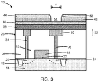
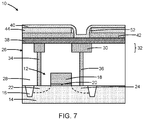
- a structure 10 includes a field-effect transistor 12 that provides an access transistor to a subsequently-formed non-volatile memory element.
- the field-effect transistor 12 may be fabricated by front-end-of-line (FEOL) processing using a substrate 14 that is composed of a single-crystal semiconductor material, such as single-crystal silicon.
- Shallow trench isolation regions 16 which may be composed of a dielectric material such as silicon dioxide, may be formed in trenches that are patterned in the substrate 14 .
- the shallow trench isolation regions 16 surround an active region of the substrate 14 in which the field-effect transistor 12 is formed.
- the field-effect transistor 12 may include a gate electrode 18 , a gate dielectric layer 20 , a source region 22 , and a drain region 24 .
- the gate electrode 18 may be composed of a heavily-doped polysilicon layer that is deposited and patterned with lithography and etching processes, and the gate dielectric layer 20 may be composed of silicon dioxide that is patterned along with the heavily-doped polysilicon layer.
- the gate electrode 18 may be a metal gate formed by a gate-first process or a replacement gate process, and the gate dielectric layer 20 may be composed of a high-k dielectric material.
- the source region 22 and drain region 24 may be doped regions that are located in the substrate 14 .
- the source region 22 and drain region 24 may be doped with an n-type dopant (e.g., phosphorus and/or arsenic) that provides n-type conductivity or, alternatively, may be doped with a p-type dopant (e.g., boron) that provides p-type conductivity.
- the field-effect transistor 12 may be a fin-type field-effect transistor, a gate-all-around field-effect transistor, etc.
- An interconnect structure 26 is formed over the field-effect transistor 12 by middle-of-line processing and back-end-of-line processing, which includes formation of contacts, vias, and wiring that is coupled with the field-effect transistor 12 .
- the interconnect structure 26 includes one or more interlayer dielectric layers 28 , a metal feature 30 in a metallization level 32 , and interconnections, such as interconnections 34 , 36 , having one or more metal islands, vias, and/or contacts arranged as metal features in the one or more interlayer dielectric layers 28 .
- the one or more interlayer dielectric layers 28 may be composed of a dielectric material, such as carbon-doped silicon dioxide, the metal feature 30 may be composed of copper, and the interconnections 34 , 36 may be composed of one or more metals, such as copper, tungsten, and/or a metal silicide.
- a dielectric material such as carbon-doped silicon dioxide
- the metal feature 30 may be composed of copper
- the interconnections 34 , 36 may be composed of one or more metals, such as copper, tungsten, and/or a metal silicide.
- a bottom electrode layer 38 is formed over the metallization level 32 . A portion of the bottom electrode layer 38 is in direct contact with the metal feature 30 .
- a resistive layer 40 is formed over the bottom electrode layer 38 . Dielectric layers 42 , 44 are formed over the resistive layer 40 . The resistive layer 40 is fully positioned between the bottom electrode layer 38 and the dielectric layer 42 .
- the resistive layer 40 is planar in that its top surface (having an interface with the dielectric layer 42 ) is planar or flat and its bottom surface (having an interface with the bottom electrode layer 38 ) is planar or flat.
- the dielectric layer 42 may directly contact the resistive layer 40
- the dielectric layer 44 may directly contact the dielectric layer 42 .
- the bottom electrode layer 38 may be composed of a metal, such as ruthenium, platinum, titanium nitride, or tantalum nitride, deposited by physical vapor deposition.
- the resistive layer 40 may be composed of a dielectric material, such as silicon dioxide, silicon nitride, or a metal oxide (e.g., magnesium oxide, tantalum oxide, hafnium oxide, titanium oxide, or aluminum oxide), deposited by chemical vapor deposition or atomic layer deposition.
- the dielectric layer 42 may be composed of dielectric material, such as silicon nitride, deposited by chemical vapor deposition or atomic layer deposition.
- the dielectric layer 44 may be composed of dielectric material, such as silicon dioxide, deposited by chemical vapor deposition or atomic layer deposition. In an embodiment, the dielectric layer 44 may be composed of silicon dioxide deposited by chemical vapor deposition using tetraethylorthosilicate (TEOS) as a reactant.
- TEOS tetrae
- the etch mask 46 is formed over the dielectric layer 44 .
- the etch mask 46 may include a layer of a photoresist that is applied by a spin-coating process, pre-baked, exposed to light projected through a photomask, baked after exposure, and developed with a chemical developer to define an opening 48 .
- the opening 48 is generally aligned with the metal feature 30 .
- an opening 50 is formed in the upper dielectric layer 44 by an etching process with the etch mask 46 ( FIG. 2 ) present.
- the dielectric layer 44 is etched at the location of the opening 48 in the etch mask 46 to form the opening 50 .
- the etching process which may be a reactive ion etching process, removes the material of the dielectric layer 44 selective to the material of the dielectric layer 42 , which functions as an etch stop.
- the terms “selective” and “selectivity” in reference to a material removal process denote that the material removal rate (i.e., etch rate) for the targeted material is higher than the material removal rate (i.e., etch rate) for at least another material exposed to the material removal.
- the etch mask 46 is stripped after the opening 50 is formed.
- Sidewall spacers 52 are formed on the sidewalls of the dielectric layer 44 inside the opening 50 .
- the sidewall spacers 52 may be formed by depositing a conformal layer of a dielectric material, such as silicon dioxide, and etching the deposited conformal layer with an anisotropic etching process, such as a reactive ion etching process.
- the etching process removes the material of the conformal layer selective to the material of the dielectric layer 42 , which again functions as an etch stop.
- the spacing, s, inside the lower portion of the opening 50 proximate to the dielectric layer 42 establishes a width dimension of a lower portion of a subsequently-formed top electrode.
- the curvature of the sidewall spacers 52 establishes a varying width dimension for an upper portion of the subsequently-formed top electrode.
- an opening 51 is formed in the dielectric layer 42 with an etching process.
- the etching process is a wet chemical etching process.
- the wet chemical etching process may utilize an etchant solution containing phosphoric acid. The etching process removes the material of the dielectric layer 42 selective to the material of the resistive layer 40 .
- the opening 51 in the dielectric layer 44 is formed at the location of the spacer-clad opening 50 in the dielectric layer 42 .
- the width dimension of the opening 51 in the dielectric layer 42 may be equal or substantially equal to the spacing, s, between the sidewall spacers 52 .
- a top electrode 54 is formed inside the openings 50 , 51 .
- the top electrode 54 may be formed by depositing a layer composed of a metal, such as ruthenium, platinum, titanium nitride, or tantalum nitride, and planarizing the deposited layer relative to the top surface of the dielectric layer 44 with chemical-mechanical polishing.
- the top electrode 54 conforms to the shape of the openings 50 , 51 and may be in direct contact at its opposite side surfaces with the sidewall spacers 52 and the sidewalls of the dielectric layer 42 below the sidewall spacers 52 .
- the top electrode 54 may have a top surface 55 that is co-planar or substantially co-planar with a top surface 45 of the dielectric layer 44 .
- the top electrode 54 has an upper portion of a given thickness or height inside the opening 50 .
- the top electrode 54 has a lower portion of a given thickness or height inside the opening 51 .
- the thickness of the upper portion of the top electrode 54 may be equal or substantially equal to the thickness of the dielectric layer 44 .
- the thickness of the lower portion of the top electrode 54 may be equal or substantially equal to the thickness of the dielectric layer 42 .
- the lower portion of the top electrode 54 is in contact with the resistive layer 40 . In an embodiment, the lower portion of the top electrode 54 may directly contact the resistive layer 40 .
- the top electrode 54 is formed without the use of reactive ion etching. Instead, the layer used to form the top electrode 54 is deposited inside the registered openings 50 , 51 and planarized.
- the opening 51 which exposes the resistive layer 40 , is formed using a wet chemical etching process, and is not formed using reactive ion etching.
- the sidewall spacers 52 are positioned between the dielectric layer 44 and the upper portion of the top electrode 54 inside the opening 50 in the dielectric layer 44 .
- the lower portion of the top electrode 54 inside the opening 51 may have a substantially constant width over its height or thickness that is equal to the width dimension, w 1 .
- the lower portion of the top electrode 54 may be have a sub-lithographic width dimension that is less than the lithography critical dimension because of the use of the sidewall spacers 53 in forming the opening 51 .
- the sidewall spacers 52 may have a curved shape such that the upper portion of the top electrode 54 inside the opening 50 has a varying width over its height or thickness.
- the width dimension of the upper portion of the top electrode 54 is narrowest at the interface with the lower portion of the top electrode 54 and widens with increasing distance from the interface. As a result, the upper portion of the top electrode 54 has a width dimension that increases with increasing distance from the lower portion of the top electrode 54 .
- the width dimension of the upper portion of the top electrode 54 has a width dimension that is greater than or equal to the width dimension of the lower portion of the top electrode 54 .
- a non-volatile memory element 56 is formed by depositing a dielectric layer 58 and patterning the layers 38 , 40 , 42 , 44 , 58 with lithography and etching processes.
- the etching process may be a reactive ion etching process.
- the patterned bottom electrode layer 38 defines a bottom electrode of the non-volatile memory element 56 and the patterned resistive layer 40 defines a switching layer of the non-volatile memory element 56 .
- the top electrode 54 is not patterned by the etching process.
- the bottom electrode layer 38 , resistive layer 40 , and dielectric layers 42 , 44 terminate at a side surface or sidewall 57 of the non-volatile memory element 56 .
- the top electrode 54 which is spaced inward from the sidewall 57 , is surrounded by the dielectric layers 42 , 44 and covered by the dielectric layer 58 during the etching process, which protects the top electrode 54 against exposure to the etching process.
- the bottom electrode is coupled to the metal feature 30 .
- the width dimension, w 1 , of the top electrode 54 is less than a width dimension, w 2 , of the bottom electrode and the resistive layer 40 .
- Additional metallization levels of the interconnect structure 26 may be formed by back-end-of-line processing over the metallization level 32 and non-volatile memory element 56 .
- the non-volatile memory element 56 may be a phase change material (PCM) memory element that include a phase change material as the switching layer.
- the phase change material may be a chalcogenide glass, such as Ge 2 Sb 2 Te 5 , and may be heated to provide an amorphous phase or a crystalline phase that respectively define the high-resistance and low-resistance states.
- the non-volatile memory element 56 may be a magnetic tunnel junction memory element.
- the non-volatile memory element may include a pinned or fixed layer, a tunnel barrier layer, and a free layer that are arranged in a layer stack between the bottom and top electrodes.
- the fixed layer may include one or more layers, such as a reference layer and a hard layer, that are composed of a magnetic material, such as a cobalt-platinum alloy or a cobalt-iron-boron alloy.
- the tunnel barrier layer may be composed of a non-magnetic, dielectric material, such as magnesium oxide or aluminum oxide.
- the free layer may include one or more layers composed of a magnetic alloy, such as a cobalt-iron-boron alloy.
- the magnetization of the reference layer of the fixed layer is pinned such that the magnetization vector cannot flip (i.e., rotate) under the influence of a programming current.
- the magnetization of the free layer is not pinned such that the magnetization vector can flip (i.e., rotate) under the influence of a programming current.
- the resistive layer 40 may be omitted from the initial layer stack formed over the metallization level 32 .
- the dielectric layer 42 is deposited directly on the bottom electrode layer 38 .
- the opening 50 in the upper dielectric layer 44 and sidewall spacers 52 are formed as previously described, and the opening 51 in the dielectric layer 42 is subsequently formed also as previously described.
- the opening 51 terminates at the bottom electrode layer 38 instead of terminating at the resistive layer, which is not yet deposited.
- the resistive layer 40 is deposited over the dielectric layer 44 and inside the openings 50 , 51 .
- the portion of the resistive layer 40 inside the opening 50 conforms to the shape of the openings 50 and sidewall spacers 52 .
- the portion of the resistive layer 40 inside the opening 50 directly contacts the bottom electrode layer 38 .
- the resistive layer 40 may have a conformal thickness.
- the top electrode 54 is formed inside the openings 50 , 51 after the resistive layer 40 is formed.
- the top electrode 54 is planarized relative to the resistive layer 40 .
- a portion of the resistive layer 40 is positioned between the top electrode 54 and the bottom electrode layer 38 .
- a non-volatile memory element 56 a is formed by depositing the dielectric layer 58 and patterning the layers 38 , 40 , 42 , 44 , 58 with lithography and etching processes, as previously described.
- the methods as described above are used in the fabrication of integrated circuit chips.
- the resulting integrated circuit chips can be distributed by the fabricator in raw wafer form (e.g., as a single wafer that has multiple unpackaged chips), as a bare die, or in a packaged form.
- the chip may be integrated with other chips, discrete circuit elements, and/or other signal processing devices as part of either an intermediate product or an end product.
- the end product can be any product that includes integrated circuit chips, such as computer products having a central processor or smartphones.
- references herein to terms modified by language of approximation such as “about”, “approximately”, and “substantially”, are not to be limited to the precise value specified.
- the language of approximation may correspond to the precision of an instrument used to measure the value and, unless otherwise dependent on the precision of the instrument, may indicate +/ ⁇ 10% of the stated value(s).
- references herein to terms such as “vertical”, “horizontal”, etc. are made by way of example, and not by way of limitation, to establish a frame of reference.
- the term “horizontal” as used herein is defined as a plane parallel to a conventional plane of a semiconductor substrate, regardless of its actual three-dimensional spatial orientation.
- the terms “vertical” and “normal” refer to a direction perpendicular to the horizontal, as just defined.
- the term “lateral” refers to a direction within the horizontal plane.
- a feature “connected” or “coupled” to or with another feature may be directly connected or coupled to or with the other feature or, instead, one or more intervening features may be present.
- a feature may be “directly connected” or “directly coupled” to or with another feature if intervening features are absent.
- a feature may be “indirectly connected” or “indirectly coupled” to or with another feature if at least one intervening feature is present.
- a feature “on” or “contacting” another feature may be directly on or in direct contact with the other feature or, instead, one or more intervening features may be present.
- a feature may be “directly on” or in “direct contact” with another feature if intervening features are absent.
- a feature may be “indirectly on” or in “indirect contact” with another feature if at least one intervening feature is present.
Landscapes
- Engineering & Computer Science (AREA)
- Manufacturing & Machinery (AREA)
- Semiconductor Memories (AREA)
Abstract
Description
- The present invention relates to integrated circuits and semiconductor device fabrication and, more specifically, to structures for a non-volatile memory element and methods of forming a structure for a non-volatile memory element.
- A resistive random-access memory (RRAM) device provides one type of embedded non-volatile memory technology. Because the memory elements of the resistive random-access memory device are non-volatile, stored bits of data are retained by a resistive random-access memory device even if the memory elements are unpowered. The non-volatility of a resistive random-access memory device contrasts with volatile memory technologies, such as a static random-access memory (SRAM) device in which the stored bits of data are eventually lost when unpowered and a dynamic random-access memory (DRAM) device in which the stored bits of data are lost if not periodically refreshed.
- Data is stored in a resistive random-access memory element by changing the resistance across a switching layer to provide different information-storage states—a high-resistance state and a low-resistance state—representing the stored bits of data. The switching layer can be modified to conduct through one or more filaments or conductive paths that are generated by applying a sufficiently high voltage across the switching layer. The filaments of the resistive random-access memory element are created or destroyed in order to respectively program the low-resistance state or the high-resistance state.
- The switching layer of a resistive random-access memory element is positioned between a bottom electrode and a top electrode. The resistive random-access memory element is formed by depositing a layer stack and then patterning the layer stack with lithography and reactive ion etching processes to successively shape the top electrode, the switching layer, and the bottom electrode. The reactive ion etching process includes a plasma component with energetic ions that can cause sputtering and redeposition of sputtered material, and that may damage the materials of the different layers.
- Improved structures for a non-volatile memory element and methods of forming a structure for a non-volatile memory element are needed.
- According to an embodiment of the invention, a structure for a non-volatile memory element is provided. The structure includes a first electrode, a switching layer positioned over the first electrode, and a dielectric layer positioned over the switching layer. The dielectric layer includes an opening extending to a first portion of the switching layer. A second electrode includes a portion in the opening in the dielectric layer. The portion of the second electrode is in contact with the first portion of the switching layer. The switching layer further includes a second portion positioned between the dielectric layer and the first electrode.
- According to another embodiment of the invention, a method of forming a structure for a non-volatile memory element is provided. The method includes depositing a first electrode layer, depositing a switching layer over the first electrode layer, depositing a dielectric layer over the switching layer, forming an opening in the dielectric layer that extends to a portion of the switching layer, and forming a second electrode including a portion in the opening in the dielectric layer. The portion of the second electrode is in contact with a first portion of the switching layer, and the switching layer includes a second portion positioned between the dielectric layer and the first electrode.
- The accompanying drawings, which are incorporated in and constitute a part of this specification, illustrate various embodiments of the invention and, together with a general description of the invention given above and the detailed description of the embodiments given below, serve to explain the embodiments of the invention. In the drawings, like reference numerals refer to like features in the various views.
-
FIG. 1 is a cross-sectional view of a structure at an initial fabrication stage of a processing method in accordance with embodiments of the invention. -
FIG. 1A is a top view of the structure ofFIG. 1 in whichFIG. 1 is taken generally along line 1-1. -
FIGS. 2-5 are cross-sectional views of the structure at successive fabrication stages subsequent toFIG. 1 . -
FIGS. 6-8 are cross-sectional views of a structure at successive fabrication stages of a processing method in accordance with alternative embodiments of the invention. - With reference to
FIGS. 1, 1A and in accordance with embodiments of the invention, astructure 10 includes a field-effect transistor 12 that provides an access transistor to a subsequently-formed non-volatile memory element. The field-effect transistor 12 may be fabricated by front-end-of-line (FEOL) processing using asubstrate 14 that is composed of a single-crystal semiconductor material, such as single-crystal silicon. Shallowtrench isolation regions 16, which may be composed of a dielectric material such as silicon dioxide, may be formed in trenches that are patterned in thesubstrate 14. The shallowtrench isolation regions 16 surround an active region of thesubstrate 14 in which the field-effect transistor 12 is formed. - The field-
effect transistor 12 may include agate electrode 18, a gatedielectric layer 20, asource region 22, and adrain region 24. Thegate electrode 18 may be composed of a heavily-doped polysilicon layer that is deposited and patterned with lithography and etching processes, and the gatedielectric layer 20 may be composed of silicon dioxide that is patterned along with the heavily-doped polysilicon layer. Alternatively, thegate electrode 18 may be a metal gate formed by a gate-first process or a replacement gate process, and the gatedielectric layer 20 may be composed of a high-k dielectric material. Thesource region 22 and drainregion 24 may be doped regions that are located in thesubstrate 14. Thesource region 22 anddrain region 24 may be doped with an n-type dopant (e.g., phosphorus and/or arsenic) that provides n-type conductivity or, alternatively, may be doped with a p-type dopant (e.g., boron) that provides p-type conductivity. Instead of having the representative planar design, the field-effect transistor 12 may be a fin-type field-effect transistor, a gate-all-around field-effect transistor, etc. - An
interconnect structure 26 is formed over the field-effect transistor 12 by middle-of-line processing and back-end-of-line processing, which includes formation of contacts, vias, and wiring that is coupled with the field-effect transistor 12. Theinterconnect structure 26 includes one or more interlayerdielectric layers 28, ametal feature 30 in ametallization level 32, and interconnections, such asinterconnections dielectric layers 28. The one or more interlayerdielectric layers 28 may be composed of a dielectric material, such as carbon-doped silicon dioxide, themetal feature 30 may be composed of copper, and theinterconnections - A
bottom electrode layer 38 is formed over themetallization level 32. A portion of thebottom electrode layer 38 is in direct contact with themetal feature 30. Aresistive layer 40 is formed over thebottom electrode layer 38.Dielectric layers resistive layer 40. Theresistive layer 40 is fully positioned between thebottom electrode layer 38 and thedielectric layer 42. Theresistive layer 40 is planar in that its top surface (having an interface with the dielectric layer 42) is planar or flat and its bottom surface (having an interface with the bottom electrode layer 38) is planar or flat. Thedielectric layer 42 may directly contact theresistive layer 40, and thedielectric layer 44 may directly contact thedielectric layer 42. - The
bottom electrode layer 38 may be composed of a metal, such as ruthenium, platinum, titanium nitride, or tantalum nitride, deposited by physical vapor deposition. Theresistive layer 40 may be composed of a dielectric material, such as silicon dioxide, silicon nitride, or a metal oxide (e.g., magnesium oxide, tantalum oxide, hafnium oxide, titanium oxide, or aluminum oxide), deposited by chemical vapor deposition or atomic layer deposition. Thedielectric layer 42 may be composed of dielectric material, such as silicon nitride, deposited by chemical vapor deposition or atomic layer deposition. Thedielectric layer 44 may be composed of dielectric material, such as silicon dioxide, deposited by chemical vapor deposition or atomic layer deposition. In an embodiment, thedielectric layer 44 may be composed of silicon dioxide deposited by chemical vapor deposition using tetraethylorthosilicate (TEOS) as a reactant. - An
etch mask 46 is formed over thedielectric layer 44. Theetch mask 46 may include a layer of a photoresist that is applied by a spin-coating process, pre-baked, exposed to light projected through a photomask, baked after exposure, and developed with a chemical developer to define an opening 48. The opening 48 is generally aligned with themetal feature 30. - With reference to
FIG. 2 in which like reference numerals refer to like features inFIG. 1 and at a subsequent fabrication stage, anopening 50 is formed in the upperdielectric layer 44 by an etching process with the etch mask 46 (FIG. 2 ) present. Thedielectric layer 44 is etched at the location of the opening 48 in theetch mask 46 to form the opening 50. - The etching process, which may be a reactive ion etching process, removes the material of the
dielectric layer 44 selective to the material of thedielectric layer 42, which functions as an etch stop. As used herein, the terms “selective” and “selectivity” in reference to a material removal process (e.g., etching) denote that the material removal rate (i.e., etch rate) for the targeted material is higher than the material removal rate (i.e., etch rate) for at least another material exposed to the material removal. Theetch mask 46 is stripped after the opening 50 is formed. -
Sidewall spacers 52 are formed on the sidewalls of thedielectric layer 44 inside theopening 50. The sidewall spacers 52 may be formed by depositing a conformal layer of a dielectric material, such as silicon dioxide, and etching the deposited conformal layer with an anisotropic etching process, such as a reactive ion etching process. The etching process removes the material of the conformal layer selective to the material of thedielectric layer 42, which again functions as an etch stop. The spacing, s, inside the lower portion of theopening 50 proximate to thedielectric layer 42 establishes a width dimension of a lower portion of a subsequently-formed top electrode. The curvature of thesidewall spacers 52 establishes a varying width dimension for an upper portion of the subsequently-formed top electrode. - With reference to
FIG. 3 in which like reference numerals refer to like features inFIG. 2 and at a subsequent fabrication stage, anopening 51 is formed in thedielectric layer 42 with an etching process. In an embodiment, the etching process is a wet chemical etching process. In an embodiment in which thedielectric layer 42 is composed of silicon nitride, the wet chemical etching process may utilize an etchant solution containing phosphoric acid. The etching process removes the material of thedielectric layer 42 selective to the material of theresistive layer 40. Theopening 51 in thedielectric layer 44 is formed at the location of the spacer-cladopening 50 in thedielectric layer 42. The width dimension of theopening 51 in thedielectric layer 42 may be equal or substantially equal to the spacing, s, between thesidewall spacers 52. - With reference to
FIG. 4 in which like reference numerals refer to like features inFIG. 3 and at a subsequent fabrication stage, atop electrode 54 is formed inside theopenings top electrode 54 may be formed by depositing a layer composed of a metal, such as ruthenium, platinum, titanium nitride, or tantalum nitride, and planarizing the deposited layer relative to the top surface of thedielectric layer 44 with chemical-mechanical polishing. Thetop electrode 54 conforms to the shape of theopenings sidewall spacers 52 and the sidewalls of thedielectric layer 42 below thesidewall spacers 52. Thetop electrode 54 may have atop surface 55 that is co-planar or substantially co-planar with atop surface 45 of thedielectric layer 44. Thetop electrode 54 has an upper portion of a given thickness or height inside theopening 50. Thetop electrode 54 has a lower portion of a given thickness or height inside theopening 51. The thickness of the upper portion of thetop electrode 54 may be equal or substantially equal to the thickness of thedielectric layer 44. The thickness of the lower portion of thetop electrode 54 may be equal or substantially equal to the thickness of thedielectric layer 42. The lower portion of thetop electrode 54 is in contact with theresistive layer 40. In an embodiment, the lower portion of thetop electrode 54 may directly contact theresistive layer 40. - Conventional process flows rely on reactive ion etching to pattern the top electrode. In contrast, the
top electrode 54 is formed without the use of reactive ion etching. Instead, the layer used to form thetop electrode 54 is deposited inside the registeredopenings opening 51, which exposes theresistive layer 40, is formed using a wet chemical etching process, and is not formed using reactive ion etching. - The sidewall spacers 52 are positioned between the
dielectric layer 44 and the upper portion of thetop electrode 54 inside theopening 50 in thedielectric layer 44. The lower portion of thetop electrode 54 inside theopening 51 may have a substantially constant width over its height or thickness that is equal to the width dimension, w1. The lower portion of thetop electrode 54 may be have a sub-lithographic width dimension that is less than the lithography critical dimension because of the use of the sidewall spacers 53 in forming theopening 51. The sidewall spacers 52 may have a curved shape such that the upper portion of thetop electrode 54 inside theopening 50 has a varying width over its height or thickness. The width dimension of the upper portion of thetop electrode 54 is narrowest at the interface with the lower portion of thetop electrode 54 and widens with increasing distance from the interface. As a result, the upper portion of thetop electrode 54 has a width dimension that increases with increasing distance from the lower portion of thetop electrode 54. The width dimension of the upper portion of thetop electrode 54 has a width dimension that is greater than or equal to the width dimension of the lower portion of thetop electrode 54. - With reference to
FIG. 5 in which like reference numerals refer to like features inFIG. 4 and at a subsequent fabrication stage, anon-volatile memory element 56 is formed by depositing adielectric layer 58 and patterning thelayers bottom electrode layer 38 defines a bottom electrode of thenon-volatile memory element 56 and the patternedresistive layer 40 defines a switching layer of thenon-volatile memory element 56. Thetop electrode 54 is not patterned by the etching process. - The
bottom electrode layer 38,resistive layer 40, anddielectric layers sidewall 57 of thenon-volatile memory element 56. Thetop electrode 54, which is spaced inward from thesidewall 57, is surrounded by thedielectric layers dielectric layer 58 during the etching process, which protects thetop electrode 54 against exposure to the etching process. The bottom electrode is coupled to themetal feature 30. The width dimension, w1, of thetop electrode 54 is less than a width dimension, w2, of the bottom electrode and theresistive layer 40. - Additional metallization levels of the
interconnect structure 26 may be formed by back-end-of-line processing over themetallization level 32 andnon-volatile memory element 56. - In an alternative embodiment, the
non-volatile memory element 56 may be a phase change material (PCM) memory element that include a phase change material as the switching layer. The phase change material may be a chalcogenide glass, such as Ge2Sb2Te5, and may be heated to provide an amorphous phase or a crystalline phase that respectively define the high-resistance and low-resistance states. - In an alternative embodiment, the
non-volatile memory element 56 may be a magnetic tunnel junction memory element. In that regard, the non-volatile memory element may include a pinned or fixed layer, a tunnel barrier layer, and a free layer that are arranged in a layer stack between the bottom and top electrodes. The fixed layer may include one or more layers, such as a reference layer and a hard layer, that are composed of a magnetic material, such as a cobalt-platinum alloy or a cobalt-iron-boron alloy. The tunnel barrier layer may be composed of a non-magnetic, dielectric material, such as magnesium oxide or aluminum oxide. The free layer may include one or more layers composed of a magnetic alloy, such as a cobalt-iron-boron alloy. The magnetization of the reference layer of the fixed layer is pinned such that the magnetization vector cannot flip (i.e., rotate) under the influence of a programming current. The magnetization of the free layer is not pinned such that the magnetization vector can flip (i.e., rotate) under the influence of a programming current. - With reference to
FIG. 6 in which like reference numerals refer to like features inFIG. 3 and in accordance with alternative embodiments of the invention, theresistive layer 40 may be omitted from the initial layer stack formed over themetallization level 32. As a result of the omission of theresistive layer 40, thedielectric layer 42 is deposited directly on thebottom electrode layer 38. Theopening 50 in theupper dielectric layer 44 andsidewall spacers 52 are formed as previously described, and theopening 51 in thedielectric layer 42 is subsequently formed also as previously described. Theopening 51 terminates at thebottom electrode layer 38 instead of terminating at the resistive layer, which is not yet deposited. - With reference to
FIG. 7 in which like reference numerals refer to like features inFIG. 6 and at a subsequent fabrication stage, theresistive layer 40 is deposited over thedielectric layer 44 and inside theopenings resistive layer 40 inside theopening 50 conforms to the shape of theopenings 50 andsidewall spacers 52. The portion of theresistive layer 40 inside theopening 50 directly contacts thebottom electrode layer 38. Theresistive layer 40 may have a conformal thickness. - With reference to
FIG. 8 in which like reference numerals refer to like features inFIG. 7 and at a subsequent fabrication stage, thetop electrode 54 is formed inside theopenings resistive layer 40 is formed. Thetop electrode 54 is planarized relative to theresistive layer 40. A portion of theresistive layer 40 is positioned between thetop electrode 54 and thebottom electrode layer 38. Anon-volatile memory element 56 a is formed by depositing thedielectric layer 58 and patterning thelayers - The methods as described above are used in the fabrication of integrated circuit chips. The resulting integrated circuit chips can be distributed by the fabricator in raw wafer form (e.g., as a single wafer that has multiple unpackaged chips), as a bare die, or in a packaged form. The chip may be integrated with other chips, discrete circuit elements, and/or other signal processing devices as part of either an intermediate product or an end product. The end product can be any product that includes integrated circuit chips, such as computer products having a central processor or smartphones.
- References herein to terms modified by language of approximation, such as “about”, “approximately”, and “substantially”, are not to be limited to the precise value specified. The language of approximation may correspond to the precision of an instrument used to measure the value and, unless otherwise dependent on the precision of the instrument, may indicate +/−10% of the stated value(s).
- References herein to terms such as “vertical”, “horizontal”, etc. are made by way of example, and not by way of limitation, to establish a frame of reference. The term “horizontal” as used herein is defined as a plane parallel to a conventional plane of a semiconductor substrate, regardless of its actual three-dimensional spatial orientation. The terms “vertical” and “normal” refer to a direction perpendicular to the horizontal, as just defined. The term “lateral” refers to a direction within the horizontal plane.
- A feature “connected” or “coupled” to or with another feature may be directly connected or coupled to or with the other feature or, instead, one or more intervening features may be present. A feature may be “directly connected” or “directly coupled” to or with another feature if intervening features are absent. A feature may be “indirectly connected” or “indirectly coupled” to or with another feature if at least one intervening feature is present. A feature “on” or “contacting” another feature may be directly on or in direct contact with the other feature or, instead, one or more intervening features may be present. A feature may be “directly on” or in “direct contact” with another feature if intervening features are absent. A feature may be “indirectly on” or in “indirect contact” with another feature if at least one intervening feature is present.
- The descriptions of the various embodiments of the present invention have been presented for purposes of illustration but are not intended to be exhaustive or limited to the embodiments disclosed. Many modifications and variations will be apparent to those of ordinary skill in the art without departing from the scope and spirit of the described embodiments. The terminology used herein was chosen to best explain the principles of the embodiments, the practical application or technical improvement over technologies found in the marketplace, or to enable others of ordinary skill in the art to understand the embodiments disclosed herein.
Claims (20)
Priority Applications (1)
| Application Number | Priority Date | Filing Date | Title |
|---|---|---|---|
| US16/846,940 US11289649B2 (en) | 2020-04-13 | 2020-04-13 | Non-volatile memory elements with a narrowed electrode |
Applications Claiming Priority (1)
| Application Number | Priority Date | Filing Date | Title |
|---|---|---|---|
| US16/846,940 US11289649B2 (en) | 2020-04-13 | 2020-04-13 | Non-volatile memory elements with a narrowed electrode |
Publications (2)
| Publication Number | Publication Date |
|---|---|
| US20210320249A1 true US20210320249A1 (en) | 2021-10-14 |
| US11289649B2 US11289649B2 (en) | 2022-03-29 |
Family
ID=78005969
Family Applications (1)
| Application Number | Title | Priority Date | Filing Date |
|---|---|---|---|
| US16/846,940 Active US11289649B2 (en) | 2020-04-13 | 2020-04-13 | Non-volatile memory elements with a narrowed electrode |
Country Status (1)
| Country | Link |
|---|---|
| US (1) | US11289649B2 (en) |
Cited By (1)
| Publication number | Priority date | Publication date | Assignee | Title |
|---|---|---|---|---|
| US20220139968A1 (en) * | 2020-11-03 | 2022-05-05 | Boe Technology Group Co., Ltd. | Display substrate, manufacturing method thereof, display panel and display device |
Family Cites Families (9)
| Publication number | Priority date | Publication date | Assignee | Title |
|---|---|---|---|---|
| US6791102B2 (en) * | 2002-12-13 | 2004-09-14 | Intel Corporation | Phase change memory |
| KR100827653B1 (en) * | 2004-12-06 | 2008-05-07 | 삼성전자주식회사 | Phase change memory cells and manufacturing methods thereof |
| KR100675279B1 (en) * | 2005-04-20 | 2007-01-26 | 삼성전자주식회사 | Phase Shift Memory Adopting Cell Diodes and Their Manufacturing Methods |
| US20060289848A1 (en) * | 2005-06-28 | 2006-12-28 | Dennison Charles H | Reducing oxidation of phase change memory electrodes |
| TWI290369B (en) * | 2005-07-08 | 2007-11-21 | Ind Tech Res Inst | Phase change memory with adjustable resistance ratio and fabricating method thereof |
| TWI273703B (en) * | 2005-08-19 | 2007-02-11 | Ind Tech Res Inst | A manufacture method and structure for improving the characteristics of phase change memory |
| US7772581B2 (en) * | 2006-09-11 | 2010-08-10 | Macronix International Co., Ltd. | Memory device having wide area phase change element and small electrode contact area |
| US20090239334A1 (en) * | 2008-03-20 | 2009-09-24 | International Business Machines Corporation | Electrode formed in aperture defined by a copolymer mask |
| US10003022B2 (en) | 2014-03-04 | 2018-06-19 | Taiwan Semiconductor Manufacturing Co., Ltd. | RRAM cell structure with conductive etch-stop layer |
-
2020
- 2020-04-13 US US16/846,940 patent/US11289649B2/en active Active
Cited By (2)
| Publication number | Priority date | Publication date | Assignee | Title |
|---|---|---|---|---|
| US20220139968A1 (en) * | 2020-11-03 | 2022-05-05 | Boe Technology Group Co., Ltd. | Display substrate, manufacturing method thereof, display panel and display device |
| US11705461B2 (en) * | 2020-11-03 | 2023-07-18 | Boe Technology Group Co., Ltd. | Display substrate, manufacturing method thereof, display panel and display device |
Also Published As
| Publication number | Publication date |
|---|---|
| US11289649B2 (en) | 2022-03-29 |
Similar Documents
| Publication | Publication Date | Title |
|---|---|---|
| US11856797B2 (en) | Resistive switching random access memory with asymmetric source and drain | |
| US7291556B2 (en) | Method for forming small features in microelectronic devices using sacrificial layers | |
| US7901979B2 (en) | Method of forming a small contact in phase-change memory | |
| US10211257B2 (en) | High density resistive random access memory (RRAM) | |
| US7834403B2 (en) | Bipolar transistor FINFET technology | |
| TW202008596A (en) | Nanosheet field effect transistor with spacers between sheets | |
| TW202036680A (en) | Methods of forming a device, and related devices and electronic systems | |
| TW202013710A (en) | Integrated chip and method of forming thereof | |
| US20130126819A1 (en) | Memory device having vertical selection transistors with shared channel structure and method for making the same | |
| TWI736272B (en) | Non-volatile memory elements with filament confinement | |
| US10109636B2 (en) | Active contact and gate contact interconnect for mitigating adjacent gate electrode shortages | |
| KR20170082732A (en) | Semiconductor devices and methods of manufacturing the same | |
| US11081640B2 (en) | Magnetic random access memory bottom electrode self-aligned to underlying interconnect structures | |
| US20150123068A1 (en) | Fin-type memory | |
| US10522395B1 (en) | Methods of forming a pattern | |
| US11289649B2 (en) | Non-volatile memory elements with a narrowed electrode | |
| TW202306168A (en) | Semiconductor structure and methods for forming the same | |
| US11502242B2 (en) | Embedded memory devices | |
| CN115528061A (en) | Semiconductor structure and forming method thereof | |
| US11075247B2 (en) | Circuit structure and method for resistive RAM with self aligned contacts in zero-via layer | |
| TW202326942A (en) | Integrated circuit device | |
| US10777607B1 (en) | Bitcells for a non-volatile memory device | |
| CN109859787B (en) | Memory circuit | |
| EP4412425B1 (en) | Layer stacks for a resistive memory element | |
| US12484234B2 (en) | Resistive random-access memory elements with lateral sidewall switching |
Legal Events
| Date | Code | Title | Description |
|---|---|---|---|
| AS | Assignment |
Owner name: GLOBALFOUNDRIES SINGAPORE PTE. LTD., SINGAPORE Free format text: ASSIGNMENT OF ASSIGNORS INTEREST;ASSIGNORS:LEONG, LUP SAN;HSIEH, CURTIS CHUN-I;TAN, JUAN BOON;AND OTHERS;SIGNING DATES FROM 20200407 TO 20200409;REEL/FRAME:052380/0631 |
|
| FEPP | Fee payment procedure |
Free format text: ENTITY STATUS SET TO UNDISCOUNTED (ORIGINAL EVENT CODE: BIG.); ENTITY STATUS OF PATENT OWNER: LARGE ENTITY |
|
| STPP | Information on status: patent application and granting procedure in general |
Free format text: FINAL REJECTION MAILED |
|
| STPP | Information on status: patent application and granting procedure in general |
Free format text: RESPONSE AFTER FINAL ACTION FORWARDED TO EXAMINER |
|
| STPP | Information on status: patent application and granting procedure in general |
Free format text: ADVISORY ACTION MAILED |
|
| STPP | Information on status: patent application and granting procedure in general |
Free format text: DOCKETED NEW CASE - READY FOR EXAMINATION |
|
| STPP | Information on status: patent application and granting procedure in general |
Free format text: NOTICE OF ALLOWANCE MAILED -- APPLICATION RECEIVED IN OFFICE OF PUBLICATIONS |
|
| STPP | Information on status: patent application and granting procedure in general |
Free format text: AWAITING TC RESP., ISSUE FEE NOT PAID |
|
| STPP | Information on status: patent application and granting procedure in general |
Free format text: NOTICE OF ALLOWANCE MAILED -- APPLICATION RECEIVED IN OFFICE OF PUBLICATIONS |
|
| STPP | Information on status: patent application and granting procedure in general |
Free format text: PUBLICATIONS -- ISSUE FEE PAYMENT VERIFIED |
|
| STCF | Information on status: patent grant |
Free format text: PATENTED CASE |
|
| MAFP | Maintenance fee payment |
Free format text: PAYMENT OF MAINTENANCE FEE, 4TH YEAR, LARGE ENTITY (ORIGINAL EVENT CODE: M1551); ENTITY STATUS OF PATENT OWNER: LARGE ENTITY Year of fee payment: 4 |