US20210028362A1 - Display devices and manufacturing method thereof - Google Patents
Display devices and manufacturing method thereof Download PDFInfo
- Publication number
- US20210028362A1 US20210028362A1 US16/871,128 US202016871128A US2021028362A1 US 20210028362 A1 US20210028362 A1 US 20210028362A1 US 202016871128 A US202016871128 A US 202016871128A US 2021028362 A1 US2021028362 A1 US 2021028362A1
- Authority
- US
- United States
- Prior art keywords
- layer
- display device
- substrate
- mother
- manufacturing
- Prior art date
- Legal status (The legal status is an assumption and is not a legal conclusion. Google has not performed a legal analysis and makes no representation as to the accuracy of the status listed.)
- Granted
Links
Images


Classifications
-
- B—PERFORMING OPERATIONS; TRANSPORTING
- B32—LAYERED PRODUCTS
- B32B—LAYERED PRODUCTS, i.e. PRODUCTS BUILT-UP OF STRATA OF FLAT OR NON-FLAT, e.g. CELLULAR OR HONEYCOMB, FORM
- B32B7/00—Layered products characterised by the relation between layers; Layered products characterised by the relative orientation of features between layers, or by the relative values of a measurable parameter between layers, i.e. products comprising layers having different physical, chemical or physicochemical properties; Layered products characterised by the interconnection of layers
- B32B7/04—Interconnection of layers
- B32B7/12—Interconnection of layers using interposed adhesives or interposed materials with bonding properties
-
- H—ELECTRICITY
- H10—SEMICONDUCTOR DEVICES; ELECTRIC SOLID-STATE DEVICES NOT OTHERWISE PROVIDED FOR
- H10H—INORGANIC LIGHT-EMITTING SEMICONDUCTOR DEVICES HAVING POTENTIAL BARRIERS
- H10H29/00—Integrated devices, or assemblies of multiple devices, comprising at least one light-emitting semiconductor element covered by group H10H20/00
- H10H29/10—Integrated devices comprising at least one light-emitting semiconductor component covered by group H10H20/00
- H10H29/14—Integrated devices comprising at least one light-emitting semiconductor component covered by group H10H20/00 comprising multiple light-emitting semiconductor components
- H10H29/142—Two-dimensional arrangements, e.g. asymmetric LED layout
-
- H01L51/003—
-
- H10P72/7402—
-
- B—PERFORMING OPERATIONS; TRANSPORTING
- B32—LAYERED PRODUCTS
- B32B—LAYERED PRODUCTS, i.e. PRODUCTS BUILT-UP OF STRATA OF FLAT OR NON-FLAT, e.g. CELLULAR OR HONEYCOMB, FORM
- B32B27/00—Layered products comprising a layer of synthetic resin
- B32B27/06—Layered products comprising a layer of synthetic resin as the main or only constituent of a layer, which is next to another layer of the same or of a different material
- B32B27/08—Layered products comprising a layer of synthetic resin as the main or only constituent of a layer, which is next to another layer of the same or of a different material of synthetic resin
-
- B—PERFORMING OPERATIONS; TRANSPORTING
- B32—LAYERED PRODUCTS
- B32B—LAYERED PRODUCTS, i.e. PRODUCTS BUILT-UP OF STRATA OF FLAT OR NON-FLAT, e.g. CELLULAR OR HONEYCOMB, FORM
- B32B27/00—Layered products comprising a layer of synthetic resin
- B32B27/28—Layered products comprising a layer of synthetic resin comprising synthetic resins not wholly covered by any one of the sub-groups B32B27/30 - B32B27/42
- B32B27/281—Layered products comprising a layer of synthetic resin comprising synthetic resins not wholly covered by any one of the sub-groups B32B27/30 - B32B27/42 comprising polyimides
-
- B—PERFORMING OPERATIONS; TRANSPORTING
- B32—LAYERED PRODUCTS
- B32B—LAYERED PRODUCTS, i.e. PRODUCTS BUILT-UP OF STRATA OF FLAT OR NON-FLAT, e.g. CELLULAR OR HONEYCOMB, FORM
- B32B27/00—Layered products comprising a layer of synthetic resin
- B32B27/36—Layered products comprising a layer of synthetic resin comprising polyesters
-
- B—PERFORMING OPERATIONS; TRANSPORTING
- B32—LAYERED PRODUCTS
- B32B—LAYERED PRODUCTS, i.e. PRODUCTS BUILT-UP OF STRATA OF FLAT OR NON-FLAT, e.g. CELLULAR OR HONEYCOMB, FORM
- B32B37/00—Methods or apparatus for laminating, e.g. by curing or by ultrasonic bonding
- B32B37/02—Methods or apparatus for laminating, e.g. by curing or by ultrasonic bonding characterised by a sequence of laminating steps, e.g. by adding new layers at consecutive laminating stations
-
- B—PERFORMING OPERATIONS; TRANSPORTING
- B32—LAYERED PRODUCTS
- B32B—LAYERED PRODUCTS, i.e. PRODUCTS BUILT-UP OF STRATA OF FLAT OR NON-FLAT, e.g. CELLULAR OR HONEYCOMB, FORM
- B32B37/00—Methods or apparatus for laminating, e.g. by curing or by ultrasonic bonding
- B32B37/12—Methods or apparatus for laminating, e.g. by curing or by ultrasonic bonding characterised by using adhesives
-
- B—PERFORMING OPERATIONS; TRANSPORTING
- B32—LAYERED PRODUCTS
- B32B—LAYERED PRODUCTS, i.e. PRODUCTS BUILT-UP OF STRATA OF FLAT OR NON-FLAT, e.g. CELLULAR OR HONEYCOMB, FORM
- B32B38/00—Ancillary operations in connection with laminating processes
- B32B38/0004—Cutting, tearing or severing, e.g. bursting; Cutter details
-
- B—PERFORMING OPERATIONS; TRANSPORTING
- B32—LAYERED PRODUCTS
- B32B—LAYERED PRODUCTS, i.e. PRODUCTS BUILT-UP OF STRATA OF FLAT OR NON-FLAT, e.g. CELLULAR OR HONEYCOMB, FORM
- B32B43/00—Operations specially adapted for layered products and not otherwise provided for, e.g. repairing; Apparatus therefor
- B32B43/006—Delaminating
-
- H01L27/3223—
-
- H01L27/3244—
-
- H01L51/0097—
-
- H01L51/56—
-
- H—ELECTRICITY
- H10—SEMICONDUCTOR DEVICES; ELECTRIC SOLID-STATE DEVICES NOT OTHERWISE PROVIDED FOR
- H10K—ORGANIC ELECTRIC SOLID-STATE DEVICES
- H10K59/00—Integrated devices, or assemblies of multiple devices, comprising at least one organic light-emitting element covered by group H10K50/00
- H10K59/10—OLED displays
- H10K59/12—Active-matrix OLED [AMOLED] displays
- H10K59/1201—Manufacture or treatment
-
- H—ELECTRICITY
- H10—SEMICONDUCTOR DEVICES; ELECTRIC SOLID-STATE DEVICES NOT OTHERWISE PROVIDED FOR
- H10K—ORGANIC ELECTRIC SOLID-STATE DEVICES
- H10K59/00—Integrated devices, or assemblies of multiple devices, comprising at least one organic light-emitting element covered by group H10K50/00
- H10K59/80—Constructional details
- H10K59/88—Dummy elements, i.e. elements having non-functional features
-
- H—ELECTRICITY
- H10—SEMICONDUCTOR DEVICES; ELECTRIC SOLID-STATE DEVICES NOT OTHERWISE PROVIDED FOR
- H10K—ORGANIC ELECTRIC SOLID-STATE DEVICES
- H10K71/00—Manufacture or treatment specially adapted for the organic devices covered by this subclass
-
- H—ELECTRICITY
- H10—SEMICONDUCTOR DEVICES; ELECTRIC SOLID-STATE DEVICES NOT OTHERWISE PROVIDED FOR
- H10K—ORGANIC ELECTRIC SOLID-STATE DEVICES
- H10K71/00—Manufacture or treatment specially adapted for the organic devices covered by this subclass
- H10K71/80—Manufacture or treatment specially adapted for the organic devices covered by this subclass using temporary substrates
-
- H—ELECTRICITY
- H10—SEMICONDUCTOR DEVICES; ELECTRIC SOLID-STATE DEVICES NOT OTHERWISE PROVIDED FOR
- H10K—ORGANIC ELECTRIC SOLID-STATE DEVICES
- H10K77/00—Constructional details of devices covered by this subclass and not covered by groups H10K10/80, H10K30/80, H10K50/80 or H10K59/80
- H10K77/10—Substrates, e.g. flexible substrates
- H10K77/111—Flexible substrates
-
- H10P14/683—
-
- H10P54/00—
-
- H10W72/013—
-
- H10W72/019—
-
- H10W72/30—
-
- H10W72/90—
-
- B32B2037/1246—
-
- B—PERFORMING OPERATIONS; TRANSPORTING
- B32—LAYERED PRODUCTS
- B32B—LAYERED PRODUCTS, i.e. PRODUCTS BUILT-UP OF STRATA OF FLAT OR NON-FLAT, e.g. CELLULAR OR HONEYCOMB, FORM
- B32B2307/00—Properties of the layers or laminate
- B32B2307/70—Other properties
- B32B2307/732—Dimensional properties
-
- B—PERFORMING OPERATIONS; TRANSPORTING
- B32—LAYERED PRODUCTS
- B32B—LAYERED PRODUCTS, i.e. PRODUCTS BUILT-UP OF STRATA OF FLAT OR NON-FLAT, e.g. CELLULAR OR HONEYCOMB, FORM
- B32B2367/00—Polyesters, e.g. PET, i.e. polyethylene terephthalate
-
- B—PERFORMING OPERATIONS; TRANSPORTING
- B32—LAYERED PRODUCTS
- B32B—LAYERED PRODUCTS, i.e. PRODUCTS BUILT-UP OF STRATA OF FLAT OR NON-FLAT, e.g. CELLULAR OR HONEYCOMB, FORM
- B32B2379/00—Other polymers having nitrogen, with or without oxygen or carbon only, in the main chain
- B32B2379/08—Polyimides
-
- B—PERFORMING OPERATIONS; TRANSPORTING
- B32—LAYERED PRODUCTS
- B32B—LAYERED PRODUCTS, i.e. PRODUCTS BUILT-UP OF STRATA OF FLAT OR NON-FLAT, e.g. CELLULAR OR HONEYCOMB, FORM
- B32B2457/00—Electrical equipment
- B32B2457/20—Displays, e.g. liquid crystal displays, plasma displays
-
- H01L2227/326—
-
- H01L2251/5338—
-
- H01L2251/566—
-
- H—ELECTRICITY
- H10—SEMICONDUCTOR DEVICES; ELECTRIC SOLID-STATE DEVICES NOT OTHERWISE PROVIDED FOR
- H10K—ORGANIC ELECTRIC SOLID-STATE DEVICES
- H10K2102/00—Constructional details relating to the organic devices covered by this subclass
- H10K2102/301—Details of OLEDs
- H10K2102/311—Flexible OLED
-
- H—ELECTRICITY
- H10—SEMICONDUCTOR DEVICES; ELECTRIC SOLID-STATE DEVICES NOT OTHERWISE PROVIDED FOR
- H10K—ORGANIC ELECTRIC SOLID-STATE DEVICES
- H10K71/00—Manufacture or treatment specially adapted for the organic devices covered by this subclass
- H10K71/851—Division of substrate
-
- H10P72/7428—
-
- Y—GENERAL TAGGING OF NEW TECHNOLOGICAL DEVELOPMENTS; GENERAL TAGGING OF CROSS-SECTIONAL TECHNOLOGIES SPANNING OVER SEVERAL SECTIONS OF THE IPC; TECHNICAL SUBJECTS COVERED BY FORMER USPC CROSS-REFERENCE ART COLLECTIONS [XRACs] AND DIGESTS
- Y02—TECHNOLOGIES OR APPLICATIONS FOR MITIGATION OR ADAPTATION AGAINST CLIMATE CHANGE
- Y02E—REDUCTION OF GREENHOUSE GAS [GHG] EMISSIONS, RELATED TO ENERGY GENERATION, TRANSMISSION OR DISTRIBUTION
- Y02E10/00—Energy generation through renewable energy sources
- Y02E10/50—Photovoltaic [PV] energy
- Y02E10/549—Organic PV cells
-
- Y—GENERAL TAGGING OF NEW TECHNOLOGICAL DEVELOPMENTS; GENERAL TAGGING OF CROSS-SECTIONAL TECHNOLOGIES SPANNING OVER SEVERAL SECTIONS OF THE IPC; TECHNICAL SUBJECTS COVERED BY FORMER USPC CROSS-REFERENCE ART COLLECTIONS [XRACs] AND DIGESTS
- Y02—TECHNOLOGIES OR APPLICATIONS FOR MITIGATION OR ADAPTATION AGAINST CLIMATE CHANGE
- Y02P—CLIMATE CHANGE MITIGATION TECHNOLOGIES IN THE PRODUCTION OR PROCESSING OF GOODS
- Y02P70/00—Climate change mitigation technologies in the production process for final industrial or consumer products
- Y02P70/50—Manufacturing or production processes characterised by the final manufactured product
Definitions
- the present disclosure relates to a display device and a manufacturing method thereof, and more particularly, to a display device and a manufacturing method thereof that may reduce occurrence of bubbles during a process of adhering a film to a rear surface of a substrate.
- a light emitting diode display as a self-emission display device has attracted attention as a device for displaying an image.
- the light emitting diode display has a self-emission characteristic and does not require an additional light source, unlike a liquid crystal display device, it is possible to reduce thickness and weight thereof. Further, the light emitting diode display has high-quality characteristics such as low power consumption, high luminance, and high response speed.
- the light emitting diode display includes a substrate, a plurality of thin film transistors disposed on the substrate, a plurality of insulating layers disposed between wires included in the thin film transistors, and a light emitting diode connected to the thin film transistors.
- Such a light emitting diode display may be manufactured through a process of forming a plurality of display devices on one substrate and then cutting them into individual display device units.
- a flexible display device has attracted attention, and thus, a flexible substrate such as polyimide is also used.
- a film or the like may be attached to a rear surface of the substrate.
- Embodiments have been made in an effort to provide a display device and a manufacturing method thereof that may reduce occurrence of bubbles during a process of adhering a film to a rear surface of a substrate.
- An embodiment of the present inventive concept provides a display device including: a mother substrate on which a plurality of display modules are located; and a mother film located on a rear surface of the mother substrate, wherein the mother film may include a first layer and a second layer disposed between the first layer and the mother substrate, the second layer has a thickness of from about 40 ⁇ m to about 60 ⁇ m, and a thickness of the first layer may be greater than that of the second layer.
- the second layer may include a pressure sensitive adhesive.
- the first layer may include polyethylene terephthalate (PET).
- PET polyethylene terephthalate
- the first layer may have a thickness of from about 60 ⁇ m to about 90 ⁇ m.
- the substrate may be a flexible substrate including polyimide.
- Another embodiment of the present inventive concept provides a manufacturing method of a display device, including: preparing a substrate including a plurality of display modules; and attaching a mother film to a rear surface of the substrate, wherein the mother film may include a first layer and a second layer disposed between the first layer and the mother substrate, and the second layer may have a thickness of from about 40 ⁇ m to about 60 ⁇ m.
- the second layer may include a pressure sensitive adhesive.
- the first layer may include polyethylene terephthalate (PET).
- PET polyethylene terephthalate
- the first layer may have a thickness of from about 60 ⁇ m to about 90 ⁇ m.
- a thickness of the first layer may be greater than that of the second layer.
- the manufacturing method of the display device may further include cutting the plurality of display modules into individual display modules, and eliminating the mother film.
- Another embodiment of the present inventive concept provides a manufacturing method of a display device, including: preparing a substrate including a plurality of display modules and a plurality dummy patterns disposed between the plurality of display modules; and cutting the substrate along a cutting line and separating the substrate into individual display modules, wherein the plurality of dummy patterns may be disposed along a direction parallel to the cutting line, and each of the plurality of dummy patterns may be provided with a groove disposed along a direction perpendicular to the cutting line.
- Each of the plurality of dummy patterns may include a first organic film and a second organic film disposed on the first organic film, and the second organic film may be partially removed along a direction perpendicular to the cutting line.
- the manufacturing method of the display device may further include an alignment mark disposed on the substrate, wherein the second organic film on the align mark is removed.
- the first organic film and the second organic film may be removed in a direction perpendicular to the cutting line.
- the plurality of dummy patterns may not overlap the cutting line.
- the plurality of dummy patterns may overlap the cutting line.
- the preparing of the substrate including the plurality of display modules and the plurality of dummy patterns disposed between the display modules may include: preparing a mother substrate including a plurality of display modules; and attaching a mother film to a rear surface of the mother substrate, wherein the mother film may include a first layer and a second layer disposed between the first layer and the mother substrate, while the second layer may include a pressure-sensitive adhesive (PSA), and a thickness of the second layer may be from about 40 ⁇ m to about 60 ⁇ m.
- PSA pressure-sensitive adhesive
- the manufacturing method of the display device may further include, after the cutting of the substrate along the cutting line to separate the substrate into individual display modules, eliminating the mother film, and attaching a protective layer to a rear surface of the substrate.
- a display device and a manufacturing method thereof that may reduce occurrence of bubbles during a process of adhering a film to a rear surface of a substrate, are provided.
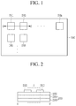
- FIG. 1 illustrates a display device according to an embodiment of the present inventive concept.
- FIG. 2 illustrates a cross-sectional view taken along line II-II′ of FIG. 1 .
- FIG. 3 illustrates an enlarged view of a portion indicated by area A of FIG. 2 in detail.
- FIG. 4 illustrates a manufacturing process of a general display device.
- FIG. 5 and FIG. 6 illustrate a principle in which bubbles occur in a display device including a second layer having a thickness of 25 ⁇ m.
- FIG. 7 illustrates a cross-sectional view of a display device according to an embodiment of the present inventive concept, which is the same as those of FIG. 5 and FIG. 6 .
- FIG. 8 illustrates a result of an experiment according to Example 1.
- FIG. 9 and FIG. 10 illustrate a process of cutting the display device of FIG. 3 , respectively.
- FIG. 11 illustrates a region where bubbles occur in a display device cut to include one display module.
- FIG. 12 schematically illustrates a manufacturing method of a display device according to an embodiment.
- FIG. 13 illustrates a top plan view and a cross-sectional view near a cutting line L 1 in a display device according to an embodiment of the present inventive concept.
- FIG. 14 illustrates an image near a cut plane of the display device according to the embodiment of FIG. 13 .
- FIG. 15 illustrates the same area as FIG. 13 in another embodiment of the present inventive concept.
- FIG. 16 illustrates the same area as FIG. 13 in another embodiment of the present inventive concept.
- FIG. 17 illustrates an image near a cut plane of the display device according to the embodiment of FIG. 16 .
- FIG. 18 illustrates the same area as FIG. 16 in another embodiment of the present inventive concept.
- FIG. 19 illustrates an image in which bubbles occur such that an alignment mark is covered according to a comparative example of the present inventive concept.
- FIG. 20 illustrates an image in which no alignment mark is covered because no bubbles occur according to an embodiment of the present inventive concept.
- FIG. 21 , FIG. 22 , FIG. 23 , and FIG. 24 illustrate the same region as FIG. 13 in a display device according to another embodiment of the present inventive concept.
- the phrase “in a plan view” means viewing a target portion from the top
- the phrase “in a cross-sectional view” means viewing a cross-section formed by vertically cutting a target portion from the side.
- the present inventive concept may solve a problem that bubbles occur during a process of adhering a film to a lower portion of a substrate in a display device and in a manufacturing process thereof.
- FIG. 1 illustrates a display device according to an embodiment of the present inventive concept.
- the display device according to the embodiment of FIG. 1 includes a plurality of display modules (DM 1 , DM 2 , DM 3 , . . . , DMn) disposed on a mother substrate 1000 . That is, FIG. 1 illustrates the display device including the plurality of display modules (DM 1 , DM 2 , DM 3 , . . . , DMn) that may separately operate, and the display device may later be cut into individual display modules to function as respective display devices.
- the mother substrate 1000 may be a flexible substrate including polyimide.
- FIG. 2 illustrates a cross-sectional view taken along line II-II′ of FIG. 1 .
- the display device according to the present embodiment includes a mother film 2000 disposed under the mother substrate 1000 .
- the mother film 2000 includes a first layer 2100 and a second layer 2200 .
- the second layer 2200 may be disposed between the first layer 2100 and the mother substrate 1000 .
- the first layer 2100 may include polyethylene terephthalate (PET).
- the second layer 2200 may include a pressure sensitive adhesive (PSA). The PSA of the second layer 2200 adheres the first layer 2100 to the mother substrate 1000 .
- the mother film 2000 may be removed after the display device including the plurality of display modules is cut into individual display modules.
- a thickness of the first layer 2100 may be 60 ⁇ m to 90 ⁇ m, and a thickness of the second layer 2200 may be 40 ⁇ m to 60 ⁇ m. In the present inventive concept, the thickness of the first layer 2100 may be greater than that of the second layer 2200 .
- the thickness of the second layer 2200 is greater than that of the first layer 2100 , a problem may occur in which an upper protective film 3000 is broken while the mother film 2000 is removed. In addition, an upper structure of the mother substrate 1000 may be damaged during the removing process of the mother film 2000 .
- the second layer 2200 including the PSA has a thickness of 40 ⁇ m to 60 ⁇ m. Therefore, because the second layer 2200 has a sufficient thickness to be able to suppress occurrence of bubbles therein, the problem that the bubbles occur in the manufacturing process of the display device may be improved.
- an effect of the present inventive concept together with the manufacturing process of the display device will be described in detail.
- a manufacturing method of a display device includes preparing a substrate including a plurality of display modules, and attaching the mother film 2000 to a rear surface of the substrate.
- the mother film 2000 includes the first layer 2100 , and the second layer 2200 disposed between the first layer 2100 and the substrate 1000 .
- the second layer 2200 may include the PSA, and its thickness may be from about 40 ⁇ m to about 60 ⁇ m.
- the manufacturing method may further include cutting the plurality of display modules into individual display modules and removing the mother film 2000 .
- the mother film 2000 includes the second layer 2200 that has a multilayer structure, includes the PSA, and has a thickness of from about 40 ⁇ m to about 60 ⁇ m, it is possible to improve the problem that the bubbles occur during the manufacturing process of the display device.
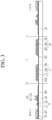
- FIG. 3 illustrates an enlarged view of a portion indicated by area A of FIG. 2 in detail.
- a first inorganic film 110 a second inorganic film 120 , an intermediate film 130 , a first organic film 140 , a second organic film 150 , and a thin film encapsulation layer 160 are disposed on the mother substrate 1000 .
- the structures of the inorganic films and the organic films are mainly shown, but a structure that is not shown may be further included.
- a display area DA, dams D 1 and D 2 , and a dummy pattern DP are disposed on the mother substrate 1000 between adjacent individual display modules.
- the display area DA includes a display module and displays an image. Types of films stacked in the display area DA, the dams D 1 and D 2 , and the dummy pattern DP may be different from each other, as shown in FIG. 3 .
- the mother substrate 1000 is cut along a first cutting line L 1 during a first cut. Thereafter, the cut mother substrate is cut along a second cutting line L 2 during a second cut. That is, only one display area DA is disposed in the cut mother substrate through the first cut along the first cutting line L 1 , and the dummy pattern DP is eliminated through the second cut along the second cutting line L 2 .
- a bezel size has been reduced, and the display area has been gradually increased.
- a distance between the display modules in the mother substrate 1000 is shortened. This means that distances between the first and second cutting lines L 1 and L 2 and the display area DA are shortened, and thus, bubbles are easily formed on the rear surface of the mother substrate 1000 , and the bubbles are not easily eliminated.
- the bubbles on the rear surface of the mother substrate 1000 are formed during the process of attaching the mother film 2000 to the mother substrate 1000 .
- FIG. 4 illustrates a manufacturing process of a general display device.
- a plurality of display modules DM 1 , DM 2 , and DM 3 are disposed on the mother substrate 1000 , and then the upper protective film 3000 is disposed thereon.
- the mother film 2000 is attached to a lower side of the mother substrate 1000 .
- the mother film 2000 is a film attached in a manufacturing process, and it may be removed in a final display device.
- the mother film 2000 may be attached by using a roller 7000 .
- In the manufacturing process it takes some time until cutting the mother film 2000 after attaching it to the display device.
- the waiting time varies depending on the manufacturing process, and it may be as short as 8 hours and as long as 100 hours or more.
- the mother film 2000 lifts from the mother substrate 1000 to generate bubbles. In FIG. 4 , the bubbles are generated between adjacent display modules which is indicated by an arrow.
- the display device and the manufacturing method thereof according to the present embodiment prevent the formation of bubbles by setting the thickness of the second layer 2200 including the PSA from about 40 ⁇ m to about 60 ⁇ m.
- FIG. 5 and FIG. 6 illustrate a principle in which bubbles occur in a display device according to a comparative example including the second layer 2200 having a thickness of about 25 ⁇ m.
- the mother film 2000 is attached to the display device by using a roller. Therefore, the mother substrate 1000 of the display device is pressed by a round surface of the roller, and is bent. This is because the mother substrate 1000 is a flexible substrate including a flexible material such as polyimide.
- the mother film 2000 is attached to the bent mother substrate 1000 , when the thickness of the second layer 2200 serving as an adhesive is not sufficiently thick, the mother film 2000 is lifted at the bent portion of the mother substrate 1000 and bubbles are formed at the bent portion of the mother substrate 1000 which are indicated by an arrow.
- FIG. 6 illustrates a cross-section of the display device in which the bubbles are formed.
- bubbles occur when the mother substrate 1000 and the mother film 2000 are separated from each other at the bent portion of the mother substrate 1000 .
- FIG. 7 illustrates a cross-sectional view of a display device according to an embodiment of the present inventive concept, which is the same portion as those of FIG. 5 and FIG. 6 .
- the thickness of the second layer 2200 of the mother film 2000 is from about 40 ⁇ m to about 60 ⁇ m, which is thicker than that of the comparative example.
- the mother substrate remains attached. Therefore, it is possible to prevent the lifting of the mother film 2000 on the curved surface of the mother substrate 1000 , and to suppress the occurrence of bubbles.
- adhesive force also increases, and thus the mother substrate 1000 and the mother film 2000 are more strongly attached to each other and are not separated.
- a bubble-occurring rate between the mother substrate 1000 and the mother film including the PSA was measured, and is shown in Table 1.
- Example 1 the thickness of the first layer 2100 including PET was about 75 ⁇ m and the thickness of the second layer 2200 including the PSA was about 50 ⁇ m.
- a bubble defect rate was measured after 32 hours had elapsed after the mother film 2000 was attached to the mother substrate 1000 .
- FIG. 8 illustrates a result of an experiment according to Example 1.
- Example 1 Stagnation time 32 h 100 h Thickness of film layer 75/50 75/50 ( ⁇ m) (PET/PSA) Mother panel bubble Not occurring 0% Not occurring 0% defect rate (0/46 substrate) (0/46 substrate)
- the measurement of the bubble defect rate was calculated by the number of substrates in which bubbles occurred among test target substrates.
- Example 1 in which the thickness of the second layer 2200 containing the PSA was about 50 ⁇ m, the phenomenon of bubble occurrence after 32 hours was improved. That is, in Example 1, no bubbles were observed in any of the 46 substrates. Referring to FIG. 8 , it was confirmed that almost no bubbles were formed in the display device. Referring back to Table 1, in the display device according to Example 1, no bubbles were observed even after 100 hours had elapsed, and it was confirmed that the phenomenon of bubble occurrence was improved.
- the display device and the manufacturing method thereof according to the present embodiment have the increased thickness of the second layer 2200 including the PSA in the mother film 2000 , so that the adhesive force between the mother substrate 1000 and the mother film 2000 is increased, and the second layer 2200 completely fills the curved portion of the mother substrate 1000 . Accordingly, it is possible to prevent the occurrence of bubbles between the mother substrate 1000 and the mother film 2000 .
- the display device and the manufacturing method thereof that are previously described relate to a mother substrate in which a plurality of display modules are formed on one substrate, and the manufacturing method of the display device according to the present embodiment includes a process of cutting the mother substrate on which the plurality of display modules are located into individual display modules.
- the manufacturing method of the display device includes preparing a substrate which includes a plurality of display modules and dummy patterns disposed between the display modules in a plan view and cutting the substrate along a cutting line to separate the substrate into individual display modules, wherein the dummy pattern is disposed along the cutting line, and a groove in which a second organic film 150 is eliminated in the dummy pattern is positioned in a direction perpendicular to the cutting line.
- the manufacturing method may further include forming a protective layer on the rear surface of the substrate. Bubbles occurring in the forming of the protective layer may be easily eliminated in the direction of the cutting line through the groove located in the dummy pattern.
- the substrate prepared in the preparing of the substrate including the plurality of display modules may be the substrate manufactured according to the manufacturing method of the foregoing embodiment. That is, the substrate prepared in the preparing of the substrate including the plurality of display modules may be a substrate manufactured by preparing the mother substrate 1000 including the plurality of display modules and attaching the mother film 2000 to the rear surface of the mother substrate 1000 .
- the mother film 2000 may include the first layer 2100 and the second layer 2200 disposed between the first layer 2100 and the substrate 1000 , and the second layer 2200 may include the PSA and have a thickness of from about 40 ⁇ m to about 60 ⁇ m.
- Bubbles may not be formed on the rear surface of the substrate including the plurality of display modules manufactured in this manner. However, even though the mother substrate is prepared without bubbles in the rear surface thereof, bubbles may be formed when the protective layer is attached after the mother substrate is cut into individual substrates.
- the manufacturing method of the display device according to the present embodiment prevents bubbles occurring in the process of attaching the protective layer after cutting the mother substrate into individual substrates.
- FIG. 9 and FIG. 10 respectively illustrate a process in which the display device of FIG. 3 is cut.
- FIG. 9 illustrates a cross-sectional view of a general display device cut along the first cutting line L 1 of FIG. 3 . Then, it is cut along the second cutting line L 2 .
- the bubbles occurring when the protective layer is attached to the rear surface of the substrate 1000 may be eliminated.
- the dummy pattern DP is disposed near the second cutting line L 2 . Therefore, a passage through which bubbles can be removed is formed when the protective layer is attached to the rear surface. That is, the bubble-eliminating passage is blocked by the dummy pattern DP, and thus the bubbles are not easily eliminated.
- the dummy pattern DP corresponds to a structure positioned on the substrate 1000 and the protective layer corresponds to a structure attached to the rear surface of the substrate, contact properties between the protective layer on the rear surface of the substrate and the substrate are affected by the structure on the substrate 1000 . Therefore, by changing a design of a structure of an upper surface of the substrate 1000 , it is possible to eliminate the bubbles in the protective layer located on the rear surface of the substrate.
- FIG. 11 illustrates a region where bubbles occur in a display device which is cut to include one display module.
- An area indicated by ‘B’ in FIG. 11 is an area where bubbles are prone to occur.
- FIG. 12 schematically illustrates a manufacturing method of a display device according to an embodiment.
- the mother film 2000 on which the plurality of display modules DM 1 , DM 2 , and DM 3 are disposed is first attached to the rear surface of the mother substrate 1000 .
- the upper protective film 3000 is formed on the plurality of display modules DM 1 , DM 2 , and DM 3 .
- the mother film 2000 may be attached by roll lamination using the roller 7000 , and the mother film 2000 may include the first layer 2100 and the second layer 2200 .
- the first layer 2100 may include PET and have a thickness of from about 60 ⁇ m to about 90 ⁇ m
- the second layer 2200 may include the PSA and may have a thickness of from about 40 ⁇ m to about 60 ⁇ m.
- the mother substrate 1000 is cut to separate the plurality of display modules into individual display modules.
- a protective layer 4000 is attached on the rear surface of the substrate 1000 from which the mother film 2000 is removed.
- the protective layer 4000 may be of a film type, and may be attached by roll lamination using the roller 7000 . Bubbles may be formed in the process of attaching the protective layer 4000 on an alignment mark of the display device, thereby obstructing a subsequent alignment process.
- the manufacturing method of the display device according to the present embodiment is a manufacturing method that may easily eliminate bubbles occurring when the protective layer 4000 is attached.
- FIG. 13 illustrates a display device according to an embodiment of the present inventive concept.
- the dummy pattern DP which includes an inorganic film 120 , an intermediate film 130 , a first organic film 140 and a second organic film 150 is disposed to overlap the cutting line L 1 .
- a portion of the second organic film 150 is removed along a direction b-b′ extending perpendicular to the cutting line L 1 to expose the first organic film 140 .
- a valley is formed between adjacent second organic films 150 .
- FIG. 14 illustrates an image near a cutting line of the display device according to the embodiment of FIG. 13 .
- the valley is indicated by an arrow.
- a width of the valley is about 0.5 mm.
- the bubbles near the cutting line may be discharged through the valley.
- FIG. 13 illustrates a structure in which the first organic film 140 which is disposed under the second organic film 140 is not removed, but in another embodiment, the first organic film 140 may also be removed. That is, as shown in FIG. 15 , when the first organic film 140 is removed, the bubbles may be well discharged through a valley formed by removing the second organic film 150 and the first organic film 140 .
- FIG. 16 illustrates the same area as FIG. 13 in another embodiment of the present inventive concept.
- the display device according to the present embodiment is the same as the display device of FIG. 13 , except that an area in which the second organic film 150 is eliminated is larger than that in FIG. 13 . A detailed description of the same components will be omitted.
- FIG. 17 illustrates an image near a cut plane of the display device according to the embodiment of FIG. 16 .
- a width of the second organic film 150 eliminated is about 4.15 nm.
- the bubble was completely eliminated, and it was confirmed that the alignment mark indicated by a dotted circle in FIG. 17 was clearly seen without being covered by the bubbles.
- FIG. 16 illustrates a structure in which the first organic film 140 is not removed and the second organic film 150 is partially removed, but the first organic film 140 may also be removed. That is, as shown in FIG. 18 , when the first organic film 140 is removed, the bubbles may be well discharged.
- FIG. 19 illustrates an image in which bubbles occur such that an alignment mark is covered by the bubbles according to a comparative example of the present inventive concept.
- FIG. 20 illustrates an image in which no alignment mark is covered by the bubbles because no bubbles occur according to an embodiment of the present inventive concept. Comparing FIG. 19 with FIG. 20 , it can be seen that in FIG. 19 , the alignment mark is covered by the bubbles, so it is hard to be recognized (see the dashed circle portion), but in FIG. 20 , there are no bubbles, so the alignment mark is clearly recognized (see the dashed circle portion).
- the area in which the second organic film 150 is recognized overlaps the alignment mark.
- the groove of the dummy pattern DP in which the second organic film 150 is recognized overlaps the alignment mark, it is possible to prevent the alignment mark from being covered by the bubbles because the bubbles are removed through the valley in which the first organic film or the second organic film 150 is removed.
- FIG. 21 to FIG. 23 illustrate display devices according to other embodiments.
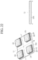
- the display device according to the present embodiment is the same as the display device according to the embodiment of FIG. 13 , except that the first organic film and the second organic film 150 in the dummy pattern DP in an area overlapping the cutting line L 1 is also removed. A detailed description of the same components will be omitted.
- the display device of FIG. 22 is the same as the display device according to the embodiment of FIG. 21 , except that both the second organic film 150 and the first organic film 140 are removed along a line e-e′ too.
- both the first organic film 140 and the second organic film 150 are removed in the direction perpendicular to the cutting line L 1 , the bubbles may be more easily removed.
- FIG. 23 is the same as that of FIG. 21 except that the first organic film 140 is not removed at the cutting line L 1 . A detailed description of the same components will be omitted.
- FIG. 24 is the same as that of FIG. 21 , except that the first organic film 140 and the second organic film 150 are eliminated in the direction perpendicular to the cutting line L 1 .
- no organic film is disposed in the passage through which the bubbles are discharged, so that the bubbles may be well discharged.
- the protective layer is a structure attached to the rear surface of the substrate 1000 and the dummy pattern DP is a structure disposed on the upper surface of the substrate, but the passage through which the bubbles formed on the rear surface of the substrate 1000 are discharged is affected by the structure disposed on the upper surface. Therefore, when the passage through which the bubbles may be discharged is formed in the dummy pattern DP as in the manufacturing method according to the present embodiment, the bubbles formed when the protective layer is attached on the rear surface of the substrate 1000 may be easily removed.
- the display device and the manufacturing method thereof by increasing the thickness of the mother film 2000 which may be removed during the manufacturing process, it is possible to improve the problem that the mother substrate 1000 and the mother film 2000 are detached from each other to form bubbles between the mother substrate 1000 and the mother film 2000 during the prolonged waiting time in the manufacturing process.
- the groove is formed in the dummy pattern near the cutting line in the direction perpendicular to the cutting line, and thus, the passage through which the bubbles formed between the mother substrate 1000 and the rear protective layer may be discharged is formed, so that the bubbles may be effectively removed.
Landscapes
- Engineering & Computer Science (AREA)
- Manufacturing & Machinery (AREA)
- Microelectronics & Electronic Packaging (AREA)
- Computer Hardware Design (AREA)
- Power Engineering (AREA)
- Devices For Indicating Variable Information By Combining Individual Elements (AREA)
- Physics & Mathematics (AREA)
- Condensed Matter Physics & Semiconductors (AREA)
- General Physics & Mathematics (AREA)
- Electroluminescent Light Sources (AREA)
Abstract
Description
- This application claims priority to and the benefit of Korean Patent Application No. 10-2019-0088330 filed in the Korean Intellectual Property Office on Jul. 22, 2019, the entire contents of which are incorporated herein by reference.
- The present disclosure relates to a display device and a manufacturing method thereof, and more particularly, to a display device and a manufacturing method thereof that may reduce occurrence of bubbles during a process of adhering a film to a rear surface of a substrate.
- Recently, a light emitting diode display as a self-emission display device has attracted attention as a device for displaying an image.
- Because the light emitting diode display has a self-emission characteristic and does not require an additional light source, unlike a liquid crystal display device, it is possible to reduce thickness and weight thereof. Further, the light emitting diode display has high-quality characteristics such as low power consumption, high luminance, and high response speed.
- Generally, the light emitting diode display includes a substrate, a plurality of thin film transistors disposed on the substrate, a plurality of insulating layers disposed between wires included in the thin film transistors, and a light emitting diode connected to the thin film transistors.
- Such a light emitting diode display may be manufactured through a process of forming a plurality of display devices on one substrate and then cutting them into individual display device units. Recently, a flexible display device has attracted attention, and thus, a flexible substrate such as polyimide is also used. In this case, in order to ensure stability of the substrate during the manufacturing process, a film or the like may be attached to a rear surface of the substrate.
- The above information disclosed in this Background section is only for enhancement of understanding of the background of the inventive concept, and therefore it may contain information that does not form the prior art that is already known in this country to a person of ordinary skill in the art.
- Embodiments have been made in an effort to provide a display device and a manufacturing method thereof that may reduce occurrence of bubbles during a process of adhering a film to a rear surface of a substrate.
- An embodiment of the present inventive concept provides a display device including: a mother substrate on which a plurality of display modules are located; and a mother film located on a rear surface of the mother substrate, wherein the mother film may include a first layer and a second layer disposed between the first layer and the mother substrate, the second layer has a thickness of from about 40 μm to about 60 μm, and a thickness of the first layer may be greater than that of the second layer.
- The second layer may include a pressure sensitive adhesive.
- The first layer may include polyethylene terephthalate (PET).
- The first layer may have a thickness of from about 60 μm to about 90 μm.
- The substrate may be a flexible substrate including polyimide.
- Another embodiment of the present inventive concept provides a manufacturing method of a display device, including: preparing a substrate including a plurality of display modules; and attaching a mother film to a rear surface of the substrate, wherein the mother film may include a first layer and a second layer disposed between the first layer and the mother substrate, and the second layer may have a thickness of from about 40 μm to about 60 μm.
- The second layer may include a pressure sensitive adhesive.
- The first layer may include polyethylene terephthalate (PET).
- The first layer may have a thickness of from about 60 μm to about 90 μm.
- A thickness of the first layer may be greater than that of the second layer.
- The manufacturing method of the display device may further include cutting the plurality of display modules into individual display modules, and eliminating the mother film.
- Another embodiment of the present inventive concept provides a manufacturing method of a display device, including: preparing a substrate including a plurality of display modules and a plurality dummy patterns disposed between the plurality of display modules; and cutting the substrate along a cutting line and separating the substrate into individual display modules, wherein the plurality of dummy patterns may be disposed along a direction parallel to the cutting line, and each of the plurality of dummy patterns may be provided with a groove disposed along a direction perpendicular to the cutting line.
- Each of the plurality of dummy patterns may include a first organic film and a second organic film disposed on the first organic film, and the second organic film may be partially removed along a direction perpendicular to the cutting line.
- The manufacturing method of the display device may further include an alignment mark disposed on the substrate, wherein the second organic film on the align mark is removed.
- The first organic film and the second organic film may be removed in a direction perpendicular to the cutting line.
- The plurality of dummy patterns may not overlap the cutting line.
- The plurality of dummy patterns may overlap the cutting line.
- The preparing of the substrate including the plurality of display modules and the plurality of dummy patterns disposed between the display modules may include: preparing a mother substrate including a plurality of display modules; and attaching a mother film to a rear surface of the mother substrate, wherein the mother film may include a first layer and a second layer disposed between the first layer and the mother substrate, while the second layer may include a pressure-sensitive adhesive (PSA), and a thickness of the second layer may be from about 40 μm to about 60 μm.
- The manufacturing method of the display device may further include, after the cutting of the substrate along the cutting line to separate the substrate into individual display modules, eliminating the mother film, and attaching a protective layer to a rear surface of the substrate.
- According to the embodiments, a display device and a manufacturing method thereof that may reduce occurrence of bubbles during a process of adhering a film to a rear surface of a substrate, are provided.
-
FIG. 1 illustrates a display device according to an embodiment of the present inventive concept. -
FIG. 2 illustrates a cross-sectional view taken along line II-II′ ofFIG. 1 . -
FIG. 3 illustrates an enlarged view of a portion indicated by area A ofFIG. 2 in detail. -
FIG. 4 illustrates a manufacturing process of a general display device. -
FIG. 5 andFIG. 6 illustrate a principle in which bubbles occur in a display device including a second layer having a thickness of 25 μm. -
FIG. 7 illustrates a cross-sectional view of a display device according to an embodiment of the present inventive concept, which is the same as those ofFIG. 5 andFIG. 6 . -
FIG. 8 illustrates a result of an experiment according to Example 1. -
FIG. 9 andFIG. 10 illustrate a process of cutting the display device ofFIG. 3 , respectively. -
FIG. 11 illustrates a region where bubbles occur in a display device cut to include one display module. -
FIG. 12 schematically illustrates a manufacturing method of a display device according to an embodiment. -
FIG. 13 illustrates a top plan view and a cross-sectional view near a cutting line L1 in a display device according to an embodiment of the present inventive concept. -
FIG. 14 illustrates an image near a cut plane of the display device according to the embodiment ofFIG. 13 . -
FIG. 15 illustrates the same area asFIG. 13 in another embodiment of the present inventive concept. -
FIG. 16 illustrates the same area asFIG. 13 in another embodiment of the present inventive concept. -
FIG. 17 illustrates an image near a cut plane of the display device according to the embodiment ofFIG. 16 . -
FIG. 18 illustrates the same area asFIG. 16 in another embodiment of the present inventive concept. -
FIG. 19 illustrates an image in which bubbles occur such that an alignment mark is covered according to a comparative example of the present inventive concept. -
FIG. 20 illustrates an image in which no alignment mark is covered because no bubbles occur according to an embodiment of the present inventive concept. -
FIG. 21 ,FIG. 22 ,FIG. 23 , andFIG. 24 illustrate the same region asFIG. 13 in a display device according to another embodiment of the present inventive concept. - The present inventive concept will be described more fully hereinafter with reference to the accompanying drawings, in which embodiments of the inventive concept are shown. As those skilled in the art would realize, the described embodiments may be modified in various different ways, all without departing from the spirit or scope of the present disclosure.
- Parts that are irrelevant to the description will be omitted to clearly describe the present disclosure, and like reference numerals designate like elements throughout the specification.
- Further, in the drawings, the size and thickness of each element are arbitrarily illustrated for ease of description, and the present disclosure is not necessarily limited to those illustrated in the drawings. In the drawings, the thicknesses of layers, films, panels, regions, etc., are exaggerated for clarity. In the drawings, for ease of description, the thicknesses of some layers and areas are exaggerated.
- It will be understood that when an element such as a layer, film, region, or substrate is referred to as being “on” another element, it can be directly on the other element or intervening elements may also be present. In contrast, when an element is referred to as being “directly on” another element, there are no intervening elements present. Further, in the specification, the word “on” or “above” means positioned on or below the object portion, and does not necessarily mean positioned on the upper side of the object portion based on a gravitational direction.
- In addition, unless explicitly described to the contrary, the word “comprise” and variations such as “comprises” or “comprising” will be understood to imply the inclusion of stated elements but not the exclusion of any other elements.
- Further, throughout the specification, the phrase “in a plan view” means viewing a target portion from the top, and the phrase “in a cross-sectional view” means viewing a cross-section formed by vertically cutting a target portion from the side.
- Hereinafter, a display device and a manufacturing method thereof according to an embodiment of the present inventive concept will be described in detail with reference to the accompanying drawings. The present inventive concept may solve a problem that bubbles occur during a process of adhering a film to a lower portion of a substrate in a display device and in a manufacturing process thereof.
-
FIG. 1 illustrates a display device according to an embodiment of the present inventive concept. The display device according to the embodiment ofFIG. 1 includes a plurality of display modules (DM1, DM2, DM3, . . . , DMn) disposed on amother substrate 1000. That is,FIG. 1 illustrates the display device including the plurality of display modules (DM1, DM2, DM3, . . . , DMn) that may separately operate, and the display device may later be cut into individual display modules to function as respective display devices. Themother substrate 1000 may be a flexible substrate including polyimide. -
FIG. 2 illustrates a cross-sectional view taken along line II-II′ ofFIG. 1 . Referring toFIG. 2 , the display device according to the present embodiment includes amother film 2000 disposed under themother substrate 1000. Themother film 2000 includes afirst layer 2100 and asecond layer 2200. Thesecond layer 2200 may be disposed between thefirst layer 2100 and themother substrate 1000. - The
first layer 2100 may include polyethylene terephthalate (PET). In addition, thesecond layer 2200 may include a pressure sensitive adhesive (PSA). The PSA of thesecond layer 2200 adheres thefirst layer 2100 to themother substrate 1000. - The
mother film 2000 may be removed after the display device including the plurality of display modules is cut into individual display modules. - In the present inventive concept, a thickness of the
first layer 2100 may be 60 μm to 90 μm, and a thickness of thesecond layer 2200 may be 40 μm to 60 μm. In the present inventive concept, the thickness of thefirst layer 2100 may be greater than that of thesecond layer 2200. When the thickness of thesecond layer 2200 is greater than that of thefirst layer 2100, a problem may occur in which an upperprotective film 3000 is broken while themother film 2000 is removed. In addition, an upper structure of themother substrate 1000 may be damaged during the removing process of themother film 2000. - In the present inventive concept, the
second layer 2200 including the PSA has a thickness of 40 μm to 60 μm. Therefore, because thesecond layer 2200 has a sufficient thickness to be able to suppress occurrence of bubbles therein, the problem that the bubbles occur in the manufacturing process of the display device may be improved. Hereinafter, an effect of the present inventive concept together with the manufacturing process of the display device will be described in detail. - A manufacturing method of a display device according to an embodiment of the present inventive concept includes preparing a substrate including a plurality of display modules, and attaching the
mother film 2000 to a rear surface of the substrate. Themother film 2000 includes thefirst layer 2100, and thesecond layer 2200 disposed between thefirst layer 2100 and thesubstrate 1000. Thesecond layer 2200 may include the PSA, and its thickness may be from about 40 μm to about 60 μm. Thereafter, the manufacturing method may further include cutting the plurality of display modules into individual display modules and removing themother film 2000. - That is, in the display device and the manufacturing method thereof according to the present inventive concept, because the
mother film 2000 includes thesecond layer 2200 that has a multilayer structure, includes the PSA, and has a thickness of from about 40 μm to about 60 μm, it is possible to improve the problem that the bubbles occur during the manufacturing process of the display device. - Hereinafter, an effect of the present inventive concept will be described in detail with reference to the accompanying drawings.
-
FIG. 3 illustrates an enlarged view of a portion indicated by area A ofFIG. 2 in detail. Referring toFIG. 3 , a firstinorganic film 110, a secondinorganic film 120, anintermediate film 130, a firstorganic film 140, a secondorganic film 150, and a thinfilm encapsulation layer 160 are disposed on themother substrate 1000. InFIG. 3 , the structures of the inorganic films and the organic films are mainly shown, but a structure that is not shown may be further included. - Referring to
FIG. 3 , a display area DA, dams D1 and D2, and a dummy pattern DP are disposed on themother substrate 1000 between adjacent individual display modules. The display area DA includes a display module and displays an image. Types of films stacked in the display area DA, the dams D1 and D2, and the dummy pattern DP may be different from each other, as shown inFIG. 3 . - Referring to
FIG. 3 , themother substrate 1000 is cut along a first cutting line L1 during a first cut. Thereafter, the cut mother substrate is cut along a second cutting line L2 during a second cut. That is, only one display area DA is disposed in the cut mother substrate through the first cut along the first cutting line L1, and the dummy pattern DP is eliminated through the second cut along the second cutting line L2. - Recently, in the display device, a bezel size has been reduced, and the display area has been gradually increased. In addition, because many display modules are prepared on one
mother substrate 1000 during a manufacturing process for cost reduction, a distance between the display modules in themother substrate 1000 is shortened. This means that distances between the first and second cutting lines L1 and L2 and the display area DA are shortened, and thus, bubbles are easily formed on the rear surface of themother substrate 1000, and the bubbles are not easily eliminated. The bubbles on the rear surface of themother substrate 1000 are formed during the process of attaching themother film 2000 to themother substrate 1000. -
FIG. 4 illustrates a manufacturing process of a general display device. Referring toFIG. 4 , a plurality of display modules DM1, DM2, and DM3 are disposed on themother substrate 1000, and then the upperprotective film 3000 is disposed thereon. - The
mother film 2000 is attached to a lower side of themother substrate 1000. Themother film 2000 is a film attached in a manufacturing process, and it may be removed in a final display device. Themother film 2000 may be attached by using aroller 7000. In the manufacturing process, it takes some time until cutting themother film 2000 after attaching it to the display device. The waiting time varies depending on the manufacturing process, and it may be as short as 8 hours and as long as 100 hours or more. During the waiting time, themother film 2000 lifts from themother substrate 1000 to generate bubbles. InFIG. 4 , the bubbles are generated between adjacent display modules which is indicated by an arrow. - However, the display device and the manufacturing method thereof according to the present embodiment prevent the formation of bubbles by setting the thickness of the
second layer 2200 including the PSA from about 40 μm to about 60 μm. -
FIG. 5 andFIG. 6 illustrate a principle in which bubbles occur in a display device according to a comparative example including thesecond layer 2200 having a thickness of about 25 μm. Referring toFIG. 5 , themother film 2000 is attached to the display device by using a roller. Therefore, themother substrate 1000 of the display device is pressed by a round surface of the roller, and is bent. This is because themother substrate 1000 is a flexible substrate including a flexible material such as polyimide. - In a case in which the
mother film 2000 is attached to thebent mother substrate 1000, when the thickness of thesecond layer 2200 serving as an adhesive is not sufficiently thick, themother film 2000 is lifted at the bent portion of themother substrate 1000 and bubbles are formed at the bent portion of themother substrate 1000 which are indicated by an arrow. -
FIG. 6 illustrates a cross-section of the display device in which the bubbles are formed. Referring toFIG. 6 , bubbles occur when themother substrate 1000 and themother film 2000 are separated from each other at the bent portion of themother substrate 1000. -
FIG. 7 illustrates a cross-sectional view of a display device according to an embodiment of the present inventive concept, which is the same portion as those ofFIG. 5 andFIG. 6 . Referring toFIG. 7 , in the display device according to the present embodiment, the thickness of thesecond layer 2200 of themother film 2000 is from about 40 μm to about 60 μm, which is thicker than that of the comparative example. - Accordingly, as shown in
FIG. 7 , as thesecond layer 2200 fills the curved surface of themother substrate 1000 without gap dispose between themother substrate 1000 and themother film 2000, the mother substrate remains attached. Therefore, it is possible to prevent the lifting of themother film 2000 on the curved surface of themother substrate 1000, and to suppress the occurrence of bubbles. In addition, as the thickness of thesecond layer 2200 increases, adhesive force also increases, and thus themother substrate 1000 and themother film 2000 are more strongly attached to each other and are not separated. - A bubble-occurring rate between the
mother substrate 1000 and the mother film including the PSA was measured, and is shown in Table 1. - In Example 1, the thickness of the
first layer 2100 including PET was about 75 μm and the thickness of thesecond layer 2200 including the PSA was about 50 μm. A bubble defect rate was measured after 32 hours had elapsed after themother film 2000 was attached to themother substrate 1000.FIG. 8 illustrates a result of an experiment according to Example 1. -
TABLE 1 Example 1 Stagnation time 32 h 100 h Thickness of film layer 75/50 75/50 (μm) (PET/PSA) Mother panel bubble Not occurring 0% Not occurring 0% defect rate (0/46 substrate) (0/46 substrate) - The measurement of the bubble defect rate was calculated by the number of substrates in which bubbles occurred among test target substrates. In Example 1 in which the thickness of the
second layer 2200 containing the PSA was about 50 μm, the phenomenon of bubble occurrence after 32 hours was improved. That is, in Example 1, no bubbles were observed in any of the 46 substrates. Referring toFIG. 8 , it was confirmed that almost no bubbles were formed in the display device. Referring back to Table 1, in the display device according to Example 1, no bubbles were observed even after 100 hours had elapsed, and it was confirmed that the phenomenon of bubble occurrence was improved. - That is, the display device and the manufacturing method thereof according to the present embodiment have the increased thickness of the
second layer 2200 including the PSA in themother film 2000, so that the adhesive force between themother substrate 1000 and themother film 2000 is increased, and thesecond layer 2200 completely fills the curved portion of themother substrate 1000. Accordingly, it is possible to prevent the occurrence of bubbles between themother substrate 1000 and themother film 2000. - Hereinafter, a manufacturing method of a display device according to another embodiment of the present inventive concept will be described. The display device and the manufacturing method thereof that are previously described relate to a mother substrate in which a plurality of display modules are formed on one substrate, and the manufacturing method of the display device according to the present embodiment includes a process of cutting the mother substrate on which the plurality of display modules are located into individual display modules.
- That is, the manufacturing method of the display device according to the present embodiment includes preparing a substrate which includes a plurality of display modules and dummy patterns disposed between the display modules in a plan view and cutting the substrate along a cutting line to separate the substrate into individual display modules, wherein the dummy pattern is disposed along the cutting line, and a groove in which a second
organic film 150 is eliminated in the dummy pattern is positioned in a direction perpendicular to the cutting line. - Thereafter, the manufacturing method may further include forming a protective layer on the rear surface of the substrate. Bubbles occurring in the forming of the protective layer may be easily eliminated in the direction of the cutting line through the groove located in the dummy pattern.
- In the present embodiment, the substrate prepared in the preparing of the substrate including the plurality of display modules may be the substrate manufactured according to the manufacturing method of the foregoing embodiment. That is, the substrate prepared in the preparing of the substrate including the plurality of display modules may be a substrate manufactured by preparing the
mother substrate 1000 including the plurality of display modules and attaching themother film 2000 to the rear surface of themother substrate 1000. - In this case, the
mother film 2000 may include thefirst layer 2100 and thesecond layer 2200 disposed between thefirst layer 2100 and thesubstrate 1000, and thesecond layer 2200 may include the PSA and have a thickness of from about 40 μm to about 60 μm. - Bubbles may not be formed on the rear surface of the substrate including the plurality of display modules manufactured in this manner. However, even though the mother substrate is prepared without bubbles in the rear surface thereof, bubbles may be formed when the protective layer is attached after the mother substrate is cut into individual substrates. The manufacturing method of the display device according to the present embodiment prevents bubbles occurring in the process of attaching the protective layer after cutting the mother substrate into individual substrates.
-
FIG. 9 andFIG. 10 respectively illustrate a process in which the display device ofFIG. 3 is cut.FIG. 9 illustrates a cross-sectional view of a general display device cut along the first cutting line L1 ofFIG. 3 . Then, it is cut along the second cutting line L2. In this case, inFIG. 9 , because a structure such as the dummy pattern DP is not disposed near the second cutting line L2, the bubbles occurring when the protective layer is attached to the rear surface of thesubstrate 1000 may be eliminated. - However, recently, because the size of a bezel of a display device is minimized, a cross-section as shown in
FIG. 10 is provided. Referring toFIG. 10 , the dummy pattern DP is disposed near the second cutting line L2. Therefore, a passage through which bubbles can be removed is formed when the protective layer is attached to the rear surface. That is, the bubble-eliminating passage is blocked by the dummy pattern DP, and thus the bubbles are not easily eliminated. This is because, although the dummy pattern DP corresponds to a structure positioned on thesubstrate 1000 and the protective layer corresponds to a structure attached to the rear surface of the substrate, contact properties between the protective layer on the rear surface of the substrate and the substrate are affected by the structure on thesubstrate 1000. Therefore, by changing a design of a structure of an upper surface of thesubstrate 1000, it is possible to eliminate the bubbles in the protective layer located on the rear surface of the substrate. -
FIG. 11 illustrates a region where bubbles occur in a display device which is cut to include one display module. An area indicated by ‘B’ inFIG. 11 is an area where bubbles are prone to occur. -
FIG. 12 schematically illustrates a manufacturing method of a display device according to an embodiment. Referring toFIG. 12 , themother film 2000 on which the plurality of display modules DM1, DM2, and DM3 are disposed is first attached to the rear surface of themother substrate 1000. The upperprotective film 3000 is formed on the plurality of display modules DM1, DM2, and DM3. - The
mother film 2000 may be attached by roll lamination using theroller 7000, and themother film 2000 may include thefirst layer 2100 and thesecond layer 2200. Thefirst layer 2100 may include PET and have a thickness of from about 60 μm to about 90 μm, and thesecond layer 2200 may include the PSA and may have a thickness of from about 40 μm to about 60 μm. - Next, referring to
FIG. 12 , themother substrate 1000 is cut to separate the plurality of display modules into individual display modules. - Then, the
mother film 2000 under themother substrate 1000 is removed. - Subsequently, a
protective layer 4000 is attached on the rear surface of thesubstrate 1000 from which themother film 2000 is removed. In this case, theprotective layer 4000 may be of a film type, and may be attached by roll lamination using theroller 7000. Bubbles may be formed in the process of attaching theprotective layer 4000 on an alignment mark of the display device, thereby obstructing a subsequent alignment process. - Thus, the manufacturing method of the display device according to the present embodiment is a manufacturing method that may easily eliminate bubbles occurring when the
protective layer 4000 is attached. -
FIG. 13 illustrates a display device according to an embodiment of the present inventive concept. Referring toFIG. 13 , the dummy pattern DP which includes aninorganic film 120, anintermediate film 130, a firstorganic film 140 and a secondorganic film 150 is disposed to overlap the cutting line L1. In this case, a portion of the secondorganic film 150 is removed along a direction b-b′ extending perpendicular to the cutting line L1 to expose the firstorganic film 140. A valley is formed between adjacent secondorganic films 150. - The bubbles may be discharged through the valley.
FIG. 14 illustrates an image near a cutting line of the display device according to the embodiment ofFIG. 13 . Referring toFIG. 14 , the valley is indicated by an arrow. In the present embodiment, a width of the valley is about 0.5 mm. As can be seen inFIG. 13 , the bubbles near the cutting line may be discharged through the valley. -
FIG. 13 illustrates a structure in which the firstorganic film 140 which is disposed under the secondorganic film 140 is not removed, but in another embodiment, the firstorganic film 140 may also be removed. That is, as shown inFIG. 15 , when the firstorganic film 140 is removed, the bubbles may be well discharged through a valley formed by removing the secondorganic film 150 and the firstorganic film 140. -
FIG. 16 illustrates the same area asFIG. 13 in another embodiment of the present inventive concept. Referring toFIG. 16 , the display device according to the present embodiment is the same as the display device ofFIG. 13 , except that an area in which the secondorganic film 150 is eliminated is larger than that inFIG. 13 . A detailed description of the same components will be omitted. -
FIG. 17 illustrates an image near a cut plane of the display device according to the embodiment ofFIG. 16 . Referring toFIG. 17 , in the display device according to the embodiment, a width of the secondorganic film 150 eliminated is about 4.15 nm. In this case, the bubble was completely eliminated, and it was confirmed that the alignment mark indicated by a dotted circle inFIG. 17 was clearly seen without being covered by the bubbles. -
FIG. 16 illustrates a structure in which the firstorganic film 140 is not removed and the secondorganic film 150 is partially removed, but the firstorganic film 140 may also be removed. That is, as shown inFIG. 18 , when the firstorganic film 140 is removed, the bubbles may be well discharged. -
FIG. 19 illustrates an image in which bubbles occur such that an alignment mark is covered by the bubbles according to a comparative example of the present inventive concept.FIG. 20 illustrates an image in which no alignment mark is covered by the bubbles because no bubbles occur according to an embodiment of the present inventive concept. ComparingFIG. 19 withFIG. 20 , it can be seen that inFIG. 19 , the alignment mark is covered by the bubbles, so it is hard to be recognized (see the dashed circle portion), but inFIG. 20 , there are no bubbles, so the alignment mark is clearly recognized (see the dashed circle portion). - Therefore, in the manufacturing method of the display device according to the present embodiment, it is desirable that the area in which the second
organic film 150 is recognized overlaps the alignment mark. When the groove of the dummy pattern DP in which the secondorganic film 150 is recognized overlaps the alignment mark, it is possible to prevent the alignment mark from being covered by the bubbles because the bubbles are removed through the valley in which the first organic film or the secondorganic film 150 is removed. -
FIG. 21 toFIG. 23 illustrate display devices according to other embodiments. Referring toFIG. 21 , the display device according to the present embodiment is the same as the display device according to the embodiment ofFIG. 13 , except that the first organic film and the secondorganic film 150 in the dummy pattern DP in an area overlapping the cutting line L1 is also removed. A detailed description of the same components will be omitted. - Referring to the cross-sectional view taken along line d-d′ of
FIG. 21 , when the portion of the secondorganic film 150 is removed and the firstorganic film 140 and the secondorganic film 150 are removed at a portion overlapping the cutting line L1, the bubbles may be more easily removed. - The display device of
FIG. 22 is the same as the display device according to the embodiment ofFIG. 21 , except that both the secondorganic film 150 and the firstorganic film 140 are removed along a line e-e′ too. InFIG. 22 , because both the firstorganic film 140 and the secondorganic film 150 are removed in the direction perpendicular to the cutting line L1, the bubbles may be more easily removed. - The embodiment of
FIG. 23 is the same as that ofFIG. 21 except that the firstorganic film 140 is not removed at the cutting line L1. A detailed description of the same components will be omitted. - The embodiment of
FIG. 24 is the same as that ofFIG. 21 , except that the firstorganic film 140 and the secondorganic film 150 are eliminated in the direction perpendicular to the cutting line L1. InFIG. 24 , no organic film is disposed in the passage through which the bubbles are discharged, so that the bubbles may be well discharged. - The protective layer is a structure attached to the rear surface of the
substrate 1000 and the dummy pattern DP is a structure disposed on the upper surface of the substrate, but the passage through which the bubbles formed on the rear surface of thesubstrate 1000 are discharged is affected by the structure disposed on the upper surface. Therefore, when the passage through which the bubbles may be discharged is formed in the dummy pattern DP as in the manufacturing method according to the present embodiment, the bubbles formed when the protective layer is attached on the rear surface of thesubstrate 1000 may be easily removed. - As described above, according to the display device and the manufacturing method thereof according to the embodiment of the present inventive concept, by increasing the thickness of the
mother film 2000 which may be removed during the manufacturing process, it is possible to improve the problem that themother substrate 1000 and themother film 2000 are detached from each other to form bubbles between themother substrate 1000 and themother film 2000 during the prolonged waiting time in the manufacturing process. In addition, the groove is formed in the dummy pattern near the cutting line in the direction perpendicular to the cutting line, and thus, the passage through which the bubbles formed between themother substrate 1000 and the rear protective layer may be discharged is formed, so that the bubbles may be effectively removed. - While this inventive concept has been described in connection with what is presently considered to be practical embodiments, it is to be understood that the inventive concept is not limited to the disclosed embodiments, but, on the contrary, is intended to cover various modifications and equivalent arrangements included within the spirit and scope of the appended claims.
Claims (20)
Applications Claiming Priority (2)
| Application Number | Priority Date | Filing Date | Title |
|---|---|---|---|
| KR1020190088330A KR102747576B1 (en) | 2019-07-22 | 2019-07-22 | Display devices and manufacturing method thereof |
| KR10-2019-0088330 | 2019-07-22 |
Publications (2)
| Publication Number | Publication Date |
|---|---|
| US20210028362A1 true US20210028362A1 (en) | 2021-01-28 |
| US12207537B2 US12207537B2 (en) | 2025-01-21 |
Family
ID=74188009
Family Applications (1)
| Application Number | Title | Priority Date | Filing Date |
|---|---|---|---|
| US16/871,128 Active 2043-07-18 US12207537B2 (en) | 2019-07-22 | 2020-05-11 | Display devices and manufacturing method thereof |
Country Status (3)
| Country | Link |
|---|---|
| US (1) | US12207537B2 (en) |
| KR (1) | KR102747576B1 (en) |
| CN (1) | CN112289827B (en) |
Citations (2)
| Publication number | Priority date | Publication date | Assignee | Title |
|---|---|---|---|---|
| US20160107425A1 (en) * | 2014-10-21 | 2016-04-21 | Nitto Europe N.V. | Pressure-sensitive adhesive film for laser beam cutting applications |
| US20170358762A1 (en) * | 2016-06-10 | 2017-12-14 | Samsung Display Co., Ltd. | Display device and method of manufacturing the same |
Family Cites Families (14)
| Publication number | Priority date | Publication date | Assignee | Title |
|---|---|---|---|---|
| KR101838756B1 (en) | 2011-12-22 | 2018-03-15 | 엘지디스플레이 주식회사 | Encapsulating method for organic electric light emission device |
| KR102104927B1 (en) | 2012-09-28 | 2020-04-28 | 삼성디스플레이 주식회사 | Organic light emitting display device and method of manufacturing the same |
| US20140091288A1 (en) | 2012-09-28 | 2014-04-03 | Samsung Display Co., Ltd. | Organic light emitting diode display and method of manufacturing the same |
| KR102010850B1 (en) | 2012-12-31 | 2019-08-14 | 엘지디스플레이 주식회사 | Method for fabricating liquid crystal panel |
| KR20140142026A (en) | 2013-06-03 | 2014-12-11 | 삼성디스플레이 주식회사 | Laminating Film and Substrate Laminated Appratus and Method of Manufacturing Organic Light Emitting Display Apparatus Using thereof |
| US9356256B2 (en) | 2013-07-31 | 2016-05-31 | Samsung Display Co., Ltd. | Flexible display device and manufacturing method thereof |
| KR20150016053A (en) * | 2013-07-31 | 2015-02-11 | 삼성디스플레이 주식회사 | Flexible display device and manufacturing method thereof |
| KR102117054B1 (en) * | 2013-08-14 | 2020-06-01 | 삼성디스플레이 주식회사 | Manufacturing method for flexible display device |
| KR20160013486A (en) | 2014-07-25 | 2016-02-04 | 삼성디스플레이 주식회사 | Mother Substrate For Display Device, Display Device and Method of manufacturing the same |
| KR102401014B1 (en) | 2015-07-01 | 2022-05-24 | 삼성디스플레이 주식회사 | Flexible display apparatus and manufacturing method thereof |
| KR102520559B1 (en) | 2016-02-03 | 2023-04-13 | 삼성디스플레이 주식회사 | Display device and method of manufacturing of the same |
| KR102548461B1 (en) | 2016-06-10 | 2023-06-28 | 삼성디스플레이 주식회사 | Display device and method for manufacturing the same |
| KR102546280B1 (en) | 2016-07-22 | 2023-06-23 | 삼성디스플레이 주식회사 | Acrylic adhesive and protective film having the same |
| KR102710447B1 (en) * | 2016-08-12 | 2024-09-27 | 삼성디스플레이 주식회사 | Organic light emitting display device |
-
2019
- 2019-07-22 KR KR1020190088330A patent/KR102747576B1/en active Active
-
2020
- 2020-05-11 US US16/871,128 patent/US12207537B2/en active Active
- 2020-07-21 CN CN202010706274.8A patent/CN112289827B/en active Active
Patent Citations (2)
| Publication number | Priority date | Publication date | Assignee | Title |
|---|---|---|---|---|
| US20160107425A1 (en) * | 2014-10-21 | 2016-04-21 | Nitto Europe N.V. | Pressure-sensitive adhesive film for laser beam cutting applications |
| US20170358762A1 (en) * | 2016-06-10 | 2017-12-14 | Samsung Display Co., Ltd. | Display device and method of manufacturing the same |
Also Published As
| Publication number | Publication date |
|---|---|
| KR102747576B1 (en) | 2024-12-27 |
| CN112289827B (en) | 2025-03-07 |
| CN112289827A (en) | 2021-01-29 |
| US12207537B2 (en) | 2025-01-21 |
| KR20210011540A (en) | 2021-02-02 |
Similar Documents
| Publication | Publication Date | Title |
|---|---|---|
| US10224289B2 (en) | Display device having an alignment mark | |
| US9722205B2 (en) | Active-matrix organic light-emitting diode (AMOLED) display panel, manufacturing method thereof and display device | |
| CN111584606B (en) | Display substrate, display device and manufacturing method thereof | |
| US20220384492A1 (en) | Array substrate, manufacturing method therefor, light-emitting substrate, and display device | |
| US20110255034A1 (en) | Display device | |
| KR20140122960A (en) | Flexible display panel | |
| TW201001001A (en) | Liquid crystal display | |
| JP2013205839A (en) | Line-on-glass type liquid crystal display device and method of fabricating the same | |
| US10515885B2 (en) | Method of fabricating a flexible display screen having substrate with a plurality of pins inserted in the through holes of lamination plate | |
| CN112786621A (en) | Flexible substrate, display panel and display device | |
| US20250143077A1 (en) | Display panel and method for manufacturing the same | |
| US20160131944A1 (en) | Display device and manufacturing method thereof | |
| CN110444697A (en) | Display panel and preparation method thereof | |
| WO2017041423A1 (en) | Array substrate and wearable device | |
| KR20150145417A (en) | Organic light emitting display device and method of manufacturing the same | |
| US20240215430A1 (en) | Stretchable display substrate and manufacturing method thereof | |
| WO2022077690A1 (en) | Support structure, flexible display panel and electronic device | |
| US12207537B2 (en) | Display devices and manufacturing method thereof | |
| CN114220932B (en) | a display device | |
| WO2020248408A1 (en) | Array substrate, display panel, and method for fabricating array substrate | |
| US12199103B2 (en) | Display panel | |
| TWI739659B (en) | Electronic device | |
| KR20170026020A (en) | Organic light emitting display device and manufacturing method thereof | |
| KR20200101551A (en) | Display device | |
| CN217983351U (en) | Displays and Electronics |
Legal Events
| Date | Code | Title | Description |
|---|---|---|---|
| AS | Assignment |
Owner name: SAMSUNG DISPLAY CO., LTD., KOREA, REPUBLIC OF Free format text: ASSIGNMENT OF ASSIGNORS INTEREST;ASSIGNORS:KIM, KWANG NYUN;BAE, KI CHUL;RYU, JONG GIL;AND OTHERS;REEL/FRAME:052630/0155 Effective date: 20191224 |
|
| FEPP | Fee payment procedure |
Free format text: ENTITY STATUS SET TO UNDISCOUNTED (ORIGINAL EVENT CODE: BIG.); ENTITY STATUS OF PATENT OWNER: LARGE ENTITY |
|
| STPP | Information on status: patent application and granting procedure in general |
Free format text: DOCKETED NEW CASE - READY FOR EXAMINATION |
|
| STPP | Information on status: patent application and granting procedure in general |
Free format text: NON FINAL ACTION MAILED |
|
| STPP | Information on status: patent application and granting procedure in general |
Free format text: NON FINAL ACTION MAILED |
|
| STPP | Information on status: patent application and granting procedure in general |
Free format text: RESPONSE TO NON-FINAL OFFICE ACTION ENTERED AND FORWARDED TO EXAMINER |
|
| STPP | Information on status: patent application and granting procedure in general |
Free format text: NON FINAL ACTION MAILED |
|
| STPP | Information on status: patent application and granting procedure in general |
Free format text: NOTICE OF ALLOWANCE MAILED -- APPLICATION RECEIVED IN OFFICE OF PUBLICATIONS |
|
| ZAAB | Notice of allowance mailed |
Free format text: ORIGINAL CODE: MN/=. |
|
| STPP | Information on status: patent application and granting procedure in general |
Free format text: PUBLICATIONS -- ISSUE FEE PAYMENT VERIFIED |
|
| STCF | Information on status: patent grant |
Free format text: PATENTED CASE |