US20190217618A1 - Method for manufacturing a fluid-ejection device with improved resonance frequency and fluid-ejection velocity, and fluid-ejection device - Google Patents
Method for manufacturing a fluid-ejection device with improved resonance frequency and fluid-ejection velocity, and fluid-ejection device Download PDFInfo
- Publication number
- US20190217618A1 US20190217618A1 US16/249,752 US201916249752A US2019217618A1 US 20190217618 A1 US20190217618 A1 US 20190217618A1 US 201916249752 A US201916249752 A US 201916249752A US 2019217618 A1 US2019217618 A1 US 2019217618A1
- Authority
- US
- United States
- Prior art keywords
- chamber
- layer
- fluid
- structural layer
- volume
- Prior art date
- Legal status (The legal status is an assumption and is not a legal conclusion. Google has not performed a legal analysis and makes no representation as to the accuracy of the status listed.)
- Granted
Links
Images


Classifications
-
- B—PERFORMING OPERATIONS; TRANSPORTING
- B41—PRINTING; LINING MACHINES; TYPEWRITERS; STAMPS
- B41J—TYPEWRITERS; SELECTIVE PRINTING MECHANISMS, i.e. MECHANISMS PRINTING OTHERWISE THAN FROM A FORME; CORRECTION OF TYPOGRAPHICAL ERRORS
- B41J2/00—Typewriters or selective printing mechanisms characterised by the printing or marking process for which they are designed
- B41J2/005—Typewriters or selective printing mechanisms characterised by the printing or marking process for which they are designed characterised by bringing liquid or particles selectively into contact with a printing material
- B41J2/01—Ink jet
- B41J2/135—Nozzles
- B41J2/14—Structure thereof only for on-demand ink jet heads
- B41J2/14201—Structure of print heads with piezoelectric elements
- B41J2/14233—Structure of print heads with piezoelectric elements of film type, deformed by bending and disposed on a diaphragm
-
- B—PERFORMING OPERATIONS; TRANSPORTING
- B41—PRINTING; LINING MACHINES; TYPEWRITERS; STAMPS
- B41J—TYPEWRITERS; SELECTIVE PRINTING MECHANISMS, i.e. MECHANISMS PRINTING OTHERWISE THAN FROM A FORME; CORRECTION OF TYPOGRAPHICAL ERRORS
- B41J2/00—Typewriters or selective printing mechanisms characterised by the printing or marking process for which they are designed
- B41J2/005—Typewriters or selective printing mechanisms characterised by the printing or marking process for which they are designed characterised by bringing liquid or particles selectively into contact with a printing material
- B41J2/01—Ink jet
- B41J2/135—Nozzles
- B41J2/16—Production of nozzles
- B41J2/1621—Manufacturing processes
- B41J2/1626—Manufacturing processes etching
-
- B—PERFORMING OPERATIONS; TRANSPORTING
- B41—PRINTING; LINING MACHINES; TYPEWRITERS; STAMPS
- B41J—TYPEWRITERS; SELECTIVE PRINTING MECHANISMS, i.e. MECHANISMS PRINTING OTHERWISE THAN FROM A FORME; CORRECTION OF TYPOGRAPHICAL ERRORS
- B41J2/00—Typewriters or selective printing mechanisms characterised by the printing or marking process for which they are designed
- B41J2/005—Typewriters or selective printing mechanisms characterised by the printing or marking process for which they are designed characterised by bringing liquid or particles selectively into contact with a printing material
- B41J2/01—Ink jet
- B41J2/135—Nozzles
- B41J2/14—Structure thereof only for on-demand ink jet heads
- B41J2/14201—Structure of print heads with piezoelectric elements
-
- B—PERFORMING OPERATIONS; TRANSPORTING
- B41—PRINTING; LINING MACHINES; TYPEWRITERS; STAMPS
- B41J—TYPEWRITERS; SELECTIVE PRINTING MECHANISMS, i.e. MECHANISMS PRINTING OTHERWISE THAN FROM A FORME; CORRECTION OF TYPOGRAPHICAL ERRORS
- B41J2/00—Typewriters or selective printing mechanisms characterised by the printing or marking process for which they are designed
- B41J2/005—Typewriters or selective printing mechanisms characterised by the printing or marking process for which they are designed characterised by bringing liquid or particles selectively into contact with a printing material
- B41J2/01—Ink jet
- B41J2/135—Nozzles
- B41J2/16—Production of nozzles
- B41J2/1606—Coating the nozzle area or the ink chamber
-
- B—PERFORMING OPERATIONS; TRANSPORTING
- B41—PRINTING; LINING MACHINES; TYPEWRITERS; STAMPS
- B41J—TYPEWRITERS; SELECTIVE PRINTING MECHANISMS, i.e. MECHANISMS PRINTING OTHERWISE THAN FROM A FORME; CORRECTION OF TYPOGRAPHICAL ERRORS
- B41J2/00—Typewriters or selective printing mechanisms characterised by the printing or marking process for which they are designed
- B41J2/005—Typewriters or selective printing mechanisms characterised by the printing or marking process for which they are designed characterised by bringing liquid or particles selectively into contact with a printing material
- B41J2/01—Ink jet
- B41J2/135—Nozzles
- B41J2/16—Production of nozzles
- B41J2/1607—Production of print heads with piezoelectric elements
- B41J2/161—Production of print heads with piezoelectric elements of film type, deformed by bending and disposed on a diaphragm
-
- B—PERFORMING OPERATIONS; TRANSPORTING
- B41—PRINTING; LINING MACHINES; TYPEWRITERS; STAMPS
- B41J—TYPEWRITERS; SELECTIVE PRINTING MECHANISMS, i.e. MECHANISMS PRINTING OTHERWISE THAN FROM A FORME; CORRECTION OF TYPOGRAPHICAL ERRORS
- B41J2/00—Typewriters or selective printing mechanisms characterised by the printing or marking process for which they are designed
- B41J2/005—Typewriters or selective printing mechanisms characterised by the printing or marking process for which they are designed characterised by bringing liquid or particles selectively into contact with a printing material
- B41J2/01—Ink jet
- B41J2/135—Nozzles
- B41J2/16—Production of nozzles
- B41J2/1621—Manufacturing processes
- B41J2/1623—Manufacturing processes bonding and adhesion
-
- B—PERFORMING OPERATIONS; TRANSPORTING
- B41—PRINTING; LINING MACHINES; TYPEWRITERS; STAMPS
- B41J—TYPEWRITERS; SELECTIVE PRINTING MECHANISMS, i.e. MECHANISMS PRINTING OTHERWISE THAN FROM A FORME; CORRECTION OF TYPOGRAPHICAL ERRORS
- B41J2/00—Typewriters or selective printing mechanisms characterised by the printing or marking process for which they are designed
- B41J2/005—Typewriters or selective printing mechanisms characterised by the printing or marking process for which they are designed characterised by bringing liquid or particles selectively into contact with a printing material
- B41J2/01—Ink jet
- B41J2/135—Nozzles
- B41J2/16—Production of nozzles
- B41J2/1621—Manufacturing processes
- B41J2/1626—Manufacturing processes etching
- B41J2/1628—Manufacturing processes etching dry etching
-
- B—PERFORMING OPERATIONS; TRANSPORTING
- B41—PRINTING; LINING MACHINES; TYPEWRITERS; STAMPS
- B41J—TYPEWRITERS; SELECTIVE PRINTING MECHANISMS, i.e. MECHANISMS PRINTING OTHERWISE THAN FROM A FORME; CORRECTION OF TYPOGRAPHICAL ERRORS
- B41J2/00—Typewriters or selective printing mechanisms characterised by the printing or marking process for which they are designed
- B41J2/005—Typewriters or selective printing mechanisms characterised by the printing or marking process for which they are designed characterised by bringing liquid or particles selectively into contact with a printing material
- B41J2/01—Ink jet
- B41J2/135—Nozzles
- B41J2/16—Production of nozzles
- B41J2/1621—Manufacturing processes
- B41J2/1626—Manufacturing processes etching
- B41J2/1629—Manufacturing processes etching wet etching
-
- B—PERFORMING OPERATIONS; TRANSPORTING
- B41—PRINTING; LINING MACHINES; TYPEWRITERS; STAMPS
- B41J—TYPEWRITERS; SELECTIVE PRINTING MECHANISMS, i.e. MECHANISMS PRINTING OTHERWISE THAN FROM A FORME; CORRECTION OF TYPOGRAPHICAL ERRORS
- B41J2/00—Typewriters or selective printing mechanisms characterised by the printing or marking process for which they are designed
- B41J2/005—Typewriters or selective printing mechanisms characterised by the printing or marking process for which they are designed characterised by bringing liquid or particles selectively into contact with a printing material
- B41J2/01—Ink jet
- B41J2/135—Nozzles
- B41J2/16—Production of nozzles
- B41J2/1621—Manufacturing processes
- B41J2/1631—Manufacturing processes photolithography
-
- B—PERFORMING OPERATIONS; TRANSPORTING
- B41—PRINTING; LINING MACHINES; TYPEWRITERS; STAMPS
- B41J—TYPEWRITERS; SELECTIVE PRINTING MECHANISMS, i.e. MECHANISMS PRINTING OTHERWISE THAN FROM A FORME; CORRECTION OF TYPOGRAPHICAL ERRORS
- B41J2/00—Typewriters or selective printing mechanisms characterised by the printing or marking process for which they are designed
- B41J2/005—Typewriters or selective printing mechanisms characterised by the printing or marking process for which they are designed characterised by bringing liquid or particles selectively into contact with a printing material
- B41J2/01—Ink jet
- B41J2/135—Nozzles
- B41J2/16—Production of nozzles
- B41J2/1621—Manufacturing processes
- B41J2/1632—Manufacturing processes machining
-
- B—PERFORMING OPERATIONS; TRANSPORTING
- B41—PRINTING; LINING MACHINES; TYPEWRITERS; STAMPS
- B41J—TYPEWRITERS; SELECTIVE PRINTING MECHANISMS, i.e. MECHANISMS PRINTING OTHERWISE THAN FROM A FORME; CORRECTION OF TYPOGRAPHICAL ERRORS
- B41J2/00—Typewriters or selective printing mechanisms characterised by the printing or marking process for which they are designed
- B41J2/005—Typewriters or selective printing mechanisms characterised by the printing or marking process for which they are designed characterised by bringing liquid or particles selectively into contact with a printing material
- B41J2/01—Ink jet
- B41J2/135—Nozzles
- B41J2/16—Production of nozzles
- B41J2/1621—Manufacturing processes
- B41J2/164—Manufacturing processes thin film formation
- B41J2/1642—Manufacturing processes thin film formation thin film formation by CVD [chemical vapor deposition]
-
- B—PERFORMING OPERATIONS; TRANSPORTING
- B81—MICROSTRUCTURAL TECHNOLOGY
- B81C—PROCESSES OR APPARATUS SPECIALLY ADAPTED FOR THE MANUFACTURE OR TREATMENT OF MICROSTRUCTURAL DEVICES OR SYSTEMS
- B81C1/00—Manufacture or treatment of devices or systems in or on a substrate
- B81C1/00015—Manufacture or treatment of devices or systems in or on a substrate for manufacturing microsystems
- B81C1/00023—Manufacture or treatment of devices or systems in or on a substrate for manufacturing microsystems without movable or flexible elements
- B81C1/00087—Holes
-
- B—PERFORMING OPERATIONS; TRANSPORTING
- B41—PRINTING; LINING MACHINES; TYPEWRITERS; STAMPS
- B41J—TYPEWRITERS; SELECTIVE PRINTING MECHANISMS, i.e. MECHANISMS PRINTING OTHERWISE THAN FROM A FORME; CORRECTION OF TYPOGRAPHICAL ERRORS
- B41J2/00—Typewriters or selective printing mechanisms characterised by the printing or marking process for which they are designed
- B41J2/005—Typewriters or selective printing mechanisms characterised by the printing or marking process for which they are designed characterised by bringing liquid or particles selectively into contact with a printing material
- B41J2/01—Ink jet
- B41J2/135—Nozzles
- B41J2/14—Structure thereof only for on-demand ink jet heads
- B41J2/14201—Structure of print heads with piezoelectric elements
- B41J2/14233—Structure of print heads with piezoelectric elements of film type, deformed by bending and disposed on a diaphragm
- B41J2002/14241—Structure of print heads with piezoelectric elements of film type, deformed by bending and disposed on a diaphragm having a cover around the piezoelectric thin film element
-
- B—PERFORMING OPERATIONS; TRANSPORTING
- B41—PRINTING; LINING MACHINES; TYPEWRITERS; STAMPS
- B41J—TYPEWRITERS; SELECTIVE PRINTING MECHANISMS, i.e. MECHANISMS PRINTING OTHERWISE THAN FROM A FORME; CORRECTION OF TYPOGRAPHICAL ERRORS
- B41J2/00—Typewriters or selective printing mechanisms characterised by the printing or marking process for which they are designed
- B41J2/005—Typewriters or selective printing mechanisms characterised by the printing or marking process for which they are designed characterised by bringing liquid or particles selectively into contact with a printing material
- B41J2/01—Ink jet
- B41J2/135—Nozzles
- B41J2/14—Structure thereof only for on-demand ink jet heads
- B41J2002/14491—Electrical connection
Definitions
- the present disclosure relates to a method for manufacturing a fluid-ejection device and to a fluid-ejection device.
- inkjet heads for printing applications.
- Similar heads may likewise be used for ejection of fluids other than ink, for example for applications in the biological or biomedical field, for local application of biological material (e.g., DNA) in the manufacture of sensors for biological analyses, for decoration of fabrics or ceramics, and in 3D-printing and additive-production applications.
- biological material e.g., DNA
- U.S. Pat. Pub. No. 2014/0313264 discloses a method for manufacturing a fluid-ejection device, which is completely provided on silicon substrates with technologies typically used for manufacturing semiconductor devices and is obtained by coupling just three wafers.
- U.S. Pat. Pub. No. 2017/182778 discloses a further method for manufacturing a fluid-ejection device of an improved type.
- the steps for manufacturing the nozzle are carried out on the corresponding wafer prior to coupling of the latter to the other wafers for formation of the finished device.
- the manufacturing process envisages coupling of just three wafers, thus reducing the risks of misalignment and limiting the manufacturing costs.
- the step of coupling between wafers envisages that they have a certain thickness greater than a minimum thickness, to enable handling thereof via the tools typically used during bonding.
- Both of the fluid-ejection devices mentioned above have a feeding channel arranged between the fluid-containment chamber and the nozzle for ejection of the fluid contained in the chamber. This channel forms a path for feeding the fluid, from the chamber to the nozzle, through a structural layer having the function of increasing the thickness of the corresponding wafer in which the channel itself is formed, for the purposes discussed above.
- the presence of the above feeding channel may cause, in given operating conditions, a deterioration of the resonance frequency of the print head and may likewise affect the velocity of fluid ejection from the nozzle, thereby reducing it.
- Embodiments are directed to a method for manufacturing a fluid-ejection device and a corresponding fluid-ejection device.
- one or more embodiments are directed to methods for manufacturing fluid-ejection heads based upon piezoelectric technology, and corresponding fluid-ejection heads based upon piezoelectric technology.
- FIG. 1 shows, in lateral sectional view, a fluid-ejection device in accordance with an embodiment of the present disclosure
- FIGS. 2-12 show steps for manufacturing the fluid-ejection device of FIG. 1 , according to one embodiment
- FIGS. 13-15 show the fluid-ejection device of FIG. 1 during respective operating steps
- FIGS. 16A and 16B show a fluid-ejection device according to another embodiment.
- Fluid-ejection devices based upon piezoelectric technology may be manufactured by bonding or gluing together a plurality of wafers previously machined by micromachining technologies typically used for manufacturing MEMS (Micro-Electro-Mechanical Systems) devices.
- a liquid-ejection device 1 is illustrated according to an aspect of the present disclosure.
- the liquid-ejection device 1 comprises a first wafer 2 , a second wafer 4 , and a third wafer 8 .
- the first wafer includes a substrate 11 and at least one piezoelectric actuator 3 , which is designed to be governed for generating a deflection of a membrane 7 coupled thereto.
- the membrane 7 extends partially suspended over at least one chamber 10 that defines a reservoir for containing fluid 6 to be expelled during use.
- the second wafer 4 defines at least one containment chamber 5 of the piezoelectric actuator 3 configured to isolate, in use, the piezoelectric actuator 3 from the fluid 6 to be ejected, and further has at least one inlet channel 9 for the fluid 6 , in fluidic connection with the chamber 10 .
- the third wafer 8 includes a body made, for example, of polysilicon (designated by the references 35 and 45 ), and at least one channel 13 for ejection of the fluid 6 (ejection nozzle), which is formed in part through the polysilicon body, provided with a hydrophilic region 42 (made, for example, of SiO 2 ), and is configured to arrange the chamber 10 in fluid communication with an environment external to the liquid-ejection device 1 .
- the aforementioned wafers 2 , 4 , 8 are coupled together by soldering-interface regions, and/or bonding regions, and/or gluing regions and/or adhesive regions, which are made, for example, of polymeric material and are designated as a whole by 15 in FIG. 1 .
- the piezoelectric actuators 3 comprise a piezoelectric region 16 arranged between a top electrode 18 and a bottom electrode 19 , designed to supply an electrical signal to the piezoelectric region 16 for generating, in use, deflection of the piezoelectric region 16 , which consequently causes deflection of the membrane 7 in a per se known manner.
- Metal paths (designated as a whole by the reference 20 ) extend from the top electrode 18 and the bottom electrode 19 towards an electrical contact region, provided with contact pads 21 designed to be biased by bonding wires (not illustrated).
- FIGS. 2-4 describe steps of micromachining of the first and second wafers 2 , 4 ;
- FIGS. 5-12 describe steps of micromachining of the third wafer 8 .
- the steps of fabrication of the first wafer 2 in brief envisage, first of all, providing the substrate 11 of semiconductor material (e.g., silicon). Then, formed on said substrate is a membrane layer 7 , for example including a stack of SiO 2 -polysilicon-SiO 2 , where the SiO 2 layers have a thickness comprised, for example, between 0.1 and 2 ⁇ m, and the polysilicon layer (grown epitaxially) has a thickness comprised between 1 and 20 ⁇ m.
- semiconductor material e.g., silicon
- a membrane layer 7 for example including a stack of SiO 2 -polysilicon-SiO 2 , where the SiO 2 layers have a thickness comprised, for example, between 0.1 and 2 ⁇ m, and the polysilicon layer (grown epitaxially) has a thickness comprised between 1 and 20 ⁇ m.
- the membrane may be made of other materials typically used for MEMS devices, for example SiO 2 or else SiN, having a thickness comprised between 0.5 and 10 ⁇ m, or else a stack in various combinations of SiO 2 —Si—SiN.
- the bottom electrode 19 of the piezoelectric actuator 3 (for example, formed by a TiO 2 layer with a thickness comprised between 5 and 50 nm, deposited on which is a Pt layer with a thickness comprised between 30 and 300 nm).
- a piezoelectric layer on top of the bottom electrode 19 by depositing a layer of PZT (Pb, Zr, TiO 3 ), having a thickness comprised between 0.5 and 3.0 ⁇ m, more typically 1 or 2 ⁇ m (which will form, after subsequent steps of definition, the piezoelectric region 16 ).
- a second layer of conductive material for example Pt or Ir or IrO2 or TiW or Ru, having a thickness comprised between 30 and 300 nm, to form the top electrode 18 .
- the electrode and piezoelectric layers are subjected to lithographic and etching steps, for patterning them according to a desired pattern, thus forming the bottom electrode 19 , the piezoelectric region 16 , and the top electrode 18 .
- One or more passivation layers 17 are then deposited on the bottom electrode 19 , the piezoelectric region 16 , and the top electrode 18 .
- the passivation layers include dielectric materials used for electrical insulation of the electrodes, for example, layers of SiO 2 , or SiN, or Al 2 O 3 , either single, or in stacks arranged on top of one another, having a thickness comprised between 10 nm and 1000.
- the passivation layers are then etched in selective regions, to creating trenches for access to the bottom electrode 19 and to the top electrode 18 .
- conductive material such as metal (e.g., aluminum or else gold, possibly together with barrier and adhesion layers such as Ti, TiN, TiW or Ta, TaN), within the trenches thus created and on the passivation layers 17 .
- a subsequent patterning step enables formation of conductive paths 23 , 25 , which enable selective access to the top electrode 18 and to the bottom electrode 19 in order to bias them electrically during use. It is further possible to form further passivation layers (e.g., of SiO 2 or SiN, not illustrated) for protecting the conductive paths 23 , 25 .
- Conductive pads 21 are likewise formed alongside the piezoelectric actuator, electrically coupled to the conductive paths 23 , 25 .
- the membrane layer 7 is selectively etched in a region thereof that extends alongside, and at a distance from, the piezoelectric actuator 3 , to expose a surface region 11 ′ of the underlying substrate 11 .
- a through hole 14 is thus formed through the membrane layer 7 , which enables, in subsequent manufacturing steps, formation of a fluidic path from outside the fluid-ejection device 1 towards the reservoir 10 , through the inlet channel 9 , as illustrated in FIG. 1 .
- the manufacturing steps envisage providing a substrate 22 of semiconductor material (e.g., silicon) with a thickness of, for example, 400 ⁇ m, which is provided with one or more dielectric layers 29 a, 29 b (e.g., layers of SiO 2 or SiN or combinations thereof) on both sides.
- a structural polysilicon layer 26 On a top face of the second wafer 4 , deposited on the dielectric layer 29 a, is a structural polysilicon layer 26 , with a thickness comprised between 1 and 20 ⁇ m, for example 4 ⁇ m.
- the second wafer 4 is etched in the region where the inlet channel 9 is to be formed by removing selective portions of the dielectric layer 29 b and of the substrate 22 throughout the thickness thereof and etching a deep trench 9 ′ (with etch stop at the dielectric layer 29 a ).
- a recess 27 a which will subsequently constitute the containment chamber 5
- a recess 27 b which, in subsequent steps, will face the region of the first wafer 2 that houses the conductive pads 21 .
- the recesses 27 a, 27 b thus formed have a depth, along Z, comprised between 50 and 300 ⁇ m.
- the first and second wafers 2 , 4 thus produced are then coupled together (e.g., by wafer-to-wafer bonding technique) so that the containment chamber 5 completely contains the piezoelectric actuator 3 and so that the through hole 14 made through the membrane 7 is aligned, and in fluidic connection, with the trench 9 ′ etched through the substrate 22 of the second wafer 4 .
- a stack of wafers is thus obtained.
- the substrate 11 of the wafer 2 is machined so as to reduce the thickness thereof.
- a step of CMP (Chemical Mechanical Polishing) or grinding is carried out in order to reach a final thickness of the substrate 11 that is, for example, comprised approximately between 5 ⁇ m and 200 ⁇ m.
- reduction of the thickness of the substrate 11 is carried out after the step of coupling between the first and second wafers 2 , 4 . In this way, handling of the wafers to enable them to be joined together is not jeopardized or rendered problematical.
- the wafer 2 is then subjected to lithographic and etching steps in a per se known manner.
- the substrate 11 of the wafer 2 is etched so as to form a cavity on the side opposite to the side that houses the piezoelectric actuator 3 , through which the silicon-oxide layer that forms the membrane 7 is exposed.
- This step enables release of the membrane 7 , rendering it suspended, and at the same time formation of a first portion 10 ′ of the chamber 10 .
- a small thickness of the substrate 11 is advantageous, in this step of definition of the membrane 7 , in so far as it enables a high control of the size of the membrane 7 in a way substantially independent of the etching technique used.
- the impact on the final size of the membrane 7 (as compared to the size defined lithographically) decreases with the reduction of the thickness of the substrate 11 (in other words, the area of the membrane 7 is all the more conformable to the photolithographic mask used, the smaller the thickness of the substrate 11 ). Control of the area of the membrane and, in particular, of its width, is important both for determination of the resonance frequency and for the volume of liquid displaced by the membrane when it is actuated.
- the thickness of the substrate 11 further defines the volume of the first portion 10 ′ of the chamber 10 .
- the volume defined by the first portion 10 ′ is comprised between 10% and 60% of the total volume designed for the chamber 10 , and more in particular between 10% and 20%.
- the third wafer 8 is provided, including a substrate 31 , for example having a thickness of approximately between 400 and 800 ⁇ m, in particular approximately 600 ⁇ m.
- the substrate 31 is made, according to an embodiment of the present disclosure, of semiconductor material, such as silicon.
- the substrate 31 has a first surface 31 a and a second surface 31 b, opposite to one another in a direction Z.
- Formed on the first surface 31 a by thermal oxidation is a first interface layer 33 , of silicon oxide (SiO 2 ).
- the step of thermal oxidation typically entails formation of an oxide layer 34 also on the back of the substrate 31 , on the second surface 31 b.
- the first interface layer 33 (and, likewise, the back oxide layer 34 ) has, for example, a thickness of approximately between 0.2 ⁇ m and 2 ⁇ m.
- FIG. 5B it is possible to form on the interface layer 33 (or as an alternative thereto) one or more further anti-wettability layers 33 ′, which have hydrophobic characteristics, i.e., are designed to provide anti-wettability functions for the nozzle 13 subsequently obtained.
- These layers are made of materials typically formed by silicon, in compounds containing hydrogen or carbon or fluorine, for example, Si x H x , SiC, SiOC.
- a nozzle layer 35 Formed on the first interface layer 33 (or on the one or more further anti-wettability layers, if present) is a nozzle layer 35 , may, for example, of epitaxially grown polysilicon, having a thickness of approximately between 10 and 75 ⁇ m.
- the nozzle layer 35 may be made of a material other than the polysilicon, for example silicon or some other material still, provided that it may be removed selectively with respect to the material of which the first interface layer 33 (or the anti-wettability layer, if present) is formed.
- a photoresist mask (not illustrated) is deposited on an exposed top surface 35 a of the nozzle layer 35 and, by subsequent lithographic and etching steps, a through hole 35 ′ is formed through the nozzle layer 35 , until a surface region of the interface layer 33 is exposed.
- said further layers are etched and removed in this process step so as to be self-aligned during complete opening of the nozzle.
- Etching is carried out using an etching chemistry capable of selectively removing the material of which the nozzle layer 35 is made (here, polysilicon), but not the material of which the interface layer 33 is made (here, silicon oxide).
- the profile of etching of the intermediate layer 35 may be controlled by choosing an etching technology and an etching chemistry in order to obtain the desired result.
- etch of a dry type RIE or DRIE
- standard silicon-etching chemistries used in the semiconductor industry SF6, HBr, etc.
- subsequent manufacturing steps envisage formation of a covering layer (reference number 42 in FIG. 7 ) on the inner walls of the through hole 35 ′, which thus causes a narrowing thereof.
- the covering layer 42 is, in particular, a layer presenting good characteristics of wettability, for example a layer of silicon oxide (SiO 2 ).
- the covering layer 42 is considered to have good characteristics of wettability when it presents a reduced angle of contact with a drop of liquid (typically, a water-based liquid or inks of different fluids) deposited thereon.
- a drop of liquid typically, a water-based liquid or inks of different fluids
- the solid-liquid interaction may be assessed in terms of angle of contact of a drop of fluid deposited on the surface considered, measured as angle formed at the surface-liquid interface. A small angle of contact is due to the tendency of the drop to flatten out on the surface, and vice versa.
- a surface is considered hydrophilic when it presents characteristics of wettability such that, when a drop is deposited thereon, the angle of contact between the surface and the drop (angle ⁇ ) has a value of less than 90°, in particular equal to or less than approximately 20° (this facilitates expulsion of any possible air bubble trapped within the chamber displacing it from the walls).
- a surface is, instead, considered as hydrophobic if it presents characteristics of wettability such that, when a drop is deposited thereon, the angle of contact between the surface and the drop (angle ⁇ ) has a value greater than 90°.
- the diameter d 1 thereof is chosen larger than the desired diameter for the ejection nozzle, as a function of the thickness envisaged for the covering layer of the inner walls of the through hole 35 ′.
- the through hole 35 ′′ has a top base opening (at the top surface 35 a of the nozzle layer 35 ) of a circular shape and with a diameter d 2 larger than the diameter d 1 of the bottom base opening (through which the interface layer 33 is exposed); i.e., it extends in the form of a conical frustum. Also in this case, since subsequent manufacturing steps envisage formation of the covering layer (reference number 42 in FIG. 7 ) on the inner walls of the through hole 35 ′′, the base diameters d 1 and d 2 are small.
- the base diameters d 1 and d 2 thereof are chosen larger than the desired value for the ejection nozzle, as a function of the thickness envisaged for the covering layer of the inner walls of the through hole 35 ′′.
- the step of formation of the through hole 35 ′ or 35 ′′, according to the respective embodiments, is followed by the step of removal of the photoresist mask and, if desired, by a step of cleaning of the top surface 35 a of the nozzle layer 35 and of the side walls internal to the through hole 35 ′, 35 ′′.
- This step carried out by removal in oxidizing environments at a high temperature (>250° C.) and/or in aggressive solvents, has the function of removing undesired polymeric layers that may form during the previous etching step.
- an optional step of thermal oxidation of the wafer 8 is carried out, for example at a temperature comprised between 800° C. and 1100° C., to form a thermal-oxide layer 38 on the nozzle layer 35 .
- This step has the function of enabling formation of the thin thermal-oxide layer 38 presenting a low surface roughness.
- the aforesaid oxide may be deposited, totally or in part, for example with techniques of a CVD type.
- the oxide layer 42 extends on the top face of the wafer 8 and within the through hole 35 ′, coating the side walls thereof.
- the thickness of the oxide layer 42 is comprised between 0.2 ⁇ m and 2 ⁇ m.
- the diameter d 3 of the through hole 35 ′ resulting after the step of formation of the oxide layer 42 has a value comprised between 1 ⁇ m and 100 ⁇ m, for example equal to 20 ⁇ m.
- a structural layer 45 formed on the oxide layer 42 is a structural layer 45 , for example of polysilicon.
- the structural layer 45 has a final thickness comprised between 5 ⁇ m and 200 ⁇ m, for example 100 ⁇ m.
- the structural layer 45 is, for instance, grown epitaxially on the oxide layer 42 and within the through hole 35 ′, until a thickness greater than the desired thickness is reached (for example, approximately 3-5 ⁇ m more), and is then subjected to a step of CMP to reduce the thickness thereof and obtain an exposed top surface with low roughness.
- a second portion 10 ′′ of the chamber 10 is followed by formation of a second portion 10 ′′ of the chamber 10 and removal of the polysilicon that, in the previous step, has filled the through hole 35 ′.
- an etching mask 50 is provided on the structural layer, and an etching step (identified by the arrows 51 ) is carried out in the region where the through hole 35 ′ had previously been formed.
- Etching is carried out with an etching chemistry designed to remove the polysilicon of which the structural layer 45 is made, but not the silicon oxide of the layer 42 .
- Etching proceeds up to complete removal of the polysilicon that extends within the through hole 35 ′ to form the second portion 10 ′′ of the chamber 10 through the structural layer 45 in fluid communication with the through opening 35 ′, as illustrated in FIG. 9 .
- the thickness of the structural layer 45 defines the volume of the second portion 10 ′′ of the chamber 10 .
- the volume defined by the second portion 10 ′′ is comprised between 90% and the 40% of the total volume designed for the chamber 10 , and more in particular between 90% and 80% (as a function of the volume of the first portion 10 ′ discussed previously).
- the stack formed by the first and second wafers 2 , 4 is coupled to the third wafer 8 via the wafer-to-wafer bonding technique using adhesive materials for the bonding 15 , which may, for example, be polymeric, or else metallic, or else vitreous.
- the third wafer 8 is coupled to the first wafer 2 so that the first and second portions 10 ′, 10 ′′ concur in forming a single fluid-containment chamber, i.e., the chamber 10 .
- the oxide layer 34 and the substrate 31 is removed. This step may be carried out by grinding the oxide layer 34 and part of the substrate 31 , or else by a chemical etch, or else by a combination of these two processes.
- the layer 33 is removed only at the top surface of the layer 35 (in the plane XY), and not along the inner walls of the nozzle 13 (for example, using an etching technique of a dry type, with an etching chemistry that is standard in semiconductor technologies).
- the layer 33 is removed on the layer 35 only at the ink-outlet nozzles.
- the step of removal of the structural layer 31 or 33 stops at the anti-wettability layer, which is not removed, or else is removed only along the walls of the nozzle 13 in the case where it were present.
- formation of the inlet channel 9 is then completed by completely removing the structural layers 26 and 29 a of the second wafer 4 .
- the fluid-ejection device of FIG. 1 is thus obtained.
- FIGS. 13-15 show the liquid-ejection device 1 in operating steps, during use.
- a first step ( FIG. 13 ) the chamber 10 is filled by a fluid 6 that is to be ejected. This step of loading of the fluid 6 is carried out through the inlet channel 9 .
- the piezoelectric actuator 3 is governed through the top and bottom electrodes 18 , 19 (which are biased by the conductive paths 23 , 25 ) so as to generate a deflection of the membrane 7 towards the inside of the chamber 10 .
- This deflection causes a movement of the fluid 6 , which, from the chamber 10 , passes directly (i.e., without intermediate channels) in the nozzle 13 , with consequent controlled ejection of a drop of fluid 6 towards the outside of the fluid-ejection device 1 .
- the piezoelectric actuator 3 is governed through the top and bottom electrodes 18 , 19 so as to generate a deflection of the membrane 7 in a direction opposite to the one illustrated in FIG. 14 so as to increase the volume of the chamber 10 , further recalling fluid 6 towards the chamber 10 through the inlet channel 9 .
- the chamber 10 is thus recharged with fluid 6 . It is thus possible to proceed cyclically by operating the piezoelectric actuator 3 for ejection of further drops of fluid.
- the steps of FIGS. 14 and 15 are then repeated throughout the printing process.
- the direct fluidic connection between the chamber 10 and the nozzle 13 enables optimization of the resonance frequency of the print head in all the operating conditions, and likewise enables an increase in the velocity of ejection of fluid from the nozzle 13 .
- the steps of production of the nozzle are carried out on the third wafer 8 prior to coupling of the latter to the first wafer 2 .
- This makes possible the use of a wide range of micromachining technologies without running the risk of damaging the coupling layers between the first and the third wafers 2 , 4 .
- it is possible to form a high-wettability layer (e.g., of silicon oxide) within the hole that defines the nozzle 13 in a simple and inexpensive way.
- the steps of production of the liquid-ejection device specify coupling of just three wafers, thus reducing the risks of misalignment in so far as just two steps of coupling of wafers are desired, thus limiting the manufacturing costs.
- the liquid-ejection device 1 a shown is the same stage of manufacture as the liquid-ejection device 1 of FIG. 12 except that the liquid-ejection device la includes a further processing step.
- the manufacturing of the liquid-ejection device la includes forming a through hole 49 in the substrate 22 to the chamber 5 .
- the chamber 5 walls, which may include the piezoelectric actuator 3 are then coated with an insulative material.
- the chamber walls, and possibly the piezoelectric actuator 3 are coated by introducing an atomic layer deposition (ALD) of a layer hafnium dioxide 50 through the through hole 49 .
- ALD atomic layer deposition
- the layer of hafnium dioxide 50 provides a barrier against humidity.
- the through hole 49 may then be closed by known methods.
- the liquid-ejection device 1 b shows a similar stage of manufacture as the liquid-ejection device la of FIG. 16A , except that the liquid-ejection device 1 b includes yet a further processing step.
- the manufacturing of the liquid-ejection device 1 b includes coating more layers of the device, such as surfaces of the chamber 10 , the trench 9 , and the nozzle 13 with the insulative layer, such as by ALD of a layer of hafnium dioxide 50 .
- the layer of hafnium dioxide may be located on outer layers of the liquid-ejection device 1 b, such as on an outer layer of substrate 22 .
- the layer of hafnium dioxide protects the surfaces, such as surfaces of the chamber and the conduits, such as the trench 9 and the nozzle 13 , against corrosive inks to be used with the device.
- the present disclosure applies, in a per se known manner to the person skilled in of the art on the basis of what has been set forth above, also to fluid-ejection devices that have, in addition to the inlet hole or channel 9 , a further recirculation hole or channel, coupled to the fluid-containment chamber 10 to enable recirculation of the fluid 6 not ejected through the nozzle 13 .
- a fluid-ejection device of this type is described, for example, in the U.S. Pat. No. 9,744,765.
Landscapes
- Engineering & Computer Science (AREA)
- Manufacturing & Machinery (AREA)
- Chemical & Material Sciences (AREA)
- Analytical Chemistry (AREA)
- Microelectronics & Electronic Packaging (AREA)
- Particle Formation And Scattering Control In Inkjet Printers (AREA)
Abstract
Description
- The present disclosure relates to a method for manufacturing a fluid-ejection device and to a fluid-ejection device.
- Known in the prior art are multiple types of fluid-ejection devices, in particular inkjet heads for printing applications. Similar heads, with appropriate modifications, may likewise be used for ejection of fluids other than ink, for example for applications in the biological or biomedical field, for local application of biological material (e.g., DNA) in the manufacture of sensors for biological analyses, for decoration of fabrics or ceramics, and in 3D-printing and additive-production applications.
- Known manufacturing methods envisage coupling via gluing or bonding of a large number of pre-machined parts; however, said method is costly and requires high precision, and the resulting device has a large thickness.
- To overcome the above drawbacks, U.S. Pat. Pub. No. 2014/0313264 discloses a method for manufacturing a fluid-ejection device, which is completely provided on silicon substrates with technologies typically used for manufacturing semiconductor devices and is obtained by coupling just three wafers.
- U.S. Pat. Pub. No. 2017/182778 discloses a further method for manufacturing a fluid-ejection device of an improved type. In particular, the steps for manufacturing the nozzle are carried out on the corresponding wafer prior to coupling of the latter to the other wafers for formation of the finished device. In addition, there is envisaged formation of a layer with high wettability within the hole that defines the nozzle in a simple and inexpensive way. Finally, also in this case, the manufacturing process envisages coupling of just three wafers, thus reducing the risks of misalignment and limiting the manufacturing costs.
- The step of coupling between wafers envisages that they have a certain thickness greater than a minimum thickness, to enable handling thereof via the tools typically used during bonding. Both of the fluid-ejection devices mentioned above have a feeding channel arranged between the fluid-containment chamber and the nozzle for ejection of the fluid contained in the chamber. This channel forms a path for feeding the fluid, from the chamber to the nozzle, through a structural layer having the function of increasing the thickness of the corresponding wafer in which the channel itself is formed, for the purposes discussed above.
- The present applicant has found that the presence of the above feeding channel may cause, in given operating conditions, a deterioration of the resonance frequency of the print head and may likewise affect the velocity of fluid ejection from the nozzle, thereby reducing it.
- Embodiments are directed to a method for manufacturing a fluid-ejection device and a corresponding fluid-ejection device. In particular, one or more embodiments are directed to methods for manufacturing fluid-ejection heads based upon piezoelectric technology, and corresponding fluid-ejection heads based upon piezoelectric technology.
- For a better understanding of the present disclosure, preferred embodiments thereof are now described, purely by way of non-limiting example, with reference to the attached drawings, wherein:
-
FIG. 1 shows, in lateral sectional view, a fluid-ejection device in accordance with an embodiment of the present disclosure; -
FIGS. 2-12 show steps for manufacturing the fluid-ejection device ofFIG. 1 , according to one embodiment; -
FIGS. 13-15 show the fluid-ejection device ofFIG. 1 during respective operating steps; and -
FIGS. 16A and 16B show a fluid-ejection device according to another embodiment. - Fluid-ejection devices based upon piezoelectric technology may be manufactured by bonding or gluing together a plurality of wafers previously machined by micromachining technologies typically used for manufacturing MEMS (Micro-Electro-Mechanical Systems) devices. In particular, with reference to
FIG. 1 , a liquid-ejection device 1 is illustrated according to an aspect of the present disclosure. With reference toFIG. 1 , the liquid-ejection device 1 comprises afirst wafer 2, asecond wafer 4, and athird wafer 8. - The first wafer includes a
substrate 11 and at least onepiezoelectric actuator 3, which is designed to be governed for generating a deflection of amembrane 7 coupled thereto. Themembrane 7 extends partially suspended over at least onechamber 10 that defines a reservoir for containingfluid 6 to be expelled during use. - The
second wafer 4 defines at least onecontainment chamber 5 of thepiezoelectric actuator 3 configured to isolate, in use, thepiezoelectric actuator 3 from thefluid 6 to be ejected, and further has at least oneinlet channel 9 for thefluid 6, in fluidic connection with thechamber 10. - The
third wafer 8 includes a body made, for example, of polysilicon (designated by thereferences 35 and 45), and at least onechannel 13 for ejection of the fluid 6 (ejection nozzle), which is formed in part through the polysilicon body, provided with a hydrophilic region 42 (made, for example, of SiO2), and is configured to arrange thechamber 10 in fluid communication with an environment external to the liquid-ejection device 1. - The
aforementioned wafers FIG. 1 . - The
piezoelectric actuators 3 comprise apiezoelectric region 16 arranged between atop electrode 18 and abottom electrode 19, designed to supply an electrical signal to thepiezoelectric region 16 for generating, in use, deflection of thepiezoelectric region 16, which consequently causes deflection of themembrane 7 in a per se known manner. Metal paths (designated as a whole by the reference 20) extend from thetop electrode 18 and thebottom electrode 19 towards an electrical contact region, provided withcontact pads 21 designed to be biased by bonding wires (not illustrated). - There now follows a description, with reference to
FIGS. 2-12 , of a process for manufacturing the fluid-ejection device 1, according to an embodiment of the present disclosure. - In particular,
FIGS. 2-4 describe steps of micromachining of the first andsecond wafers FIGS. 5-12 describe steps of micromachining of thethird wafer 8. - In particular, with reference to
FIG. 2 , the steps of fabrication of thefirst wafer 2 in brief envisage, first of all, providing thesubstrate 11 of semiconductor material (e.g., silicon). Then, formed on said substrate is amembrane layer 7, for example including a stack of SiO2-polysilicon-SiO2, where the SiO2 layers have a thickness comprised, for example, between 0.1 and 2 μm, and the polysilicon layer (grown epitaxially) has a thickness comprised between 1 and 20 μm. In various embodiments, the membrane may be made of other materials typically used for MEMS devices, for example SiO2 or else SiN, having a thickness comprised between 0.5 and 10 μm, or else a stack in various combinations of SiO2—Si—SiN. - This is followed by formation, on the
membrane layer 7, of thebottom electrode 19 of the piezoelectric actuator 3 (for example, formed by a TiO2 layer with a thickness comprised between 5 and 50 nm, deposited on which is a Pt layer with a thickness comprised between 30 and 300 nm). - There then follows deposition of a piezoelectric layer on top of the
bottom electrode 19 by depositing a layer of PZT (Pb, Zr, TiO3), having a thickness comprised between 0.5 and 3.0 μm, more typically 1 or 2 μm (which will form, after subsequent steps of definition, the piezoelectric region 16). Next, deposited on the piezoelectric layer is a second layer of conductive material, for example Pt or Ir or IrO2 or TiW or Ru, having a thickness comprised between 30 and 300 nm, to form thetop electrode 18. - The electrode and piezoelectric layers are subjected to lithographic and etching steps, for patterning them according to a desired pattern, thus forming the
bottom electrode 19, thepiezoelectric region 16, and thetop electrode 18. - One or
more passivation layers 17 are then deposited on thebottom electrode 19, thepiezoelectric region 16, and thetop electrode 18. The passivation layers include dielectric materials used for electrical insulation of the electrodes, for example, layers of SiO2, or SiN, or Al2O3, either single, or in stacks arranged on top of one another, having a thickness comprised between 10 nm and 1000. The passivation layers are then etched in selective regions, to creating trenches for access to thebottom electrode 19 and to thetop electrode 18. This is then followed by a step of deposition of conductive material, such as metal (e.g., aluminum or else gold, possibly together with barrier and adhesion layers such as Ti, TiN, TiW or Ta, TaN), within the trenches thus created and on thepassivation layers 17. A subsequent patterning step enables formation ofconductive paths top electrode 18 and to thebottom electrode 19 in order to bias them electrically during use. It is further possible to form further passivation layers (e.g., of SiO2 or SiN, not illustrated) for protecting theconductive paths Conductive pads 21 are likewise formed alongside the piezoelectric actuator, electrically coupled to theconductive paths - Finally, the
membrane layer 7 is selectively etched in a region thereof that extends alongside, and at a distance from, thepiezoelectric actuator 3, to expose asurface region 11′ of theunderlying substrate 11. A throughhole 14 is thus formed through themembrane layer 7, which enables, in subsequent manufacturing steps, formation of a fluidic path from outside the fluid-ejection device 1 towards thereservoir 10, through theinlet channel 9, as illustrated inFIG. 1 . - With reference to the second wafer 4 (illustrated in
FIG. 3 ), the manufacturing steps envisage providing asubstrate 22 of semiconductor material (e.g., silicon) with a thickness of, for example, 400 μm, which is provided with one or moredielectric layers second wafer 4, deposited on thedielectric layer 29 a, is astructural polysilicon layer 26, with a thickness comprised between 1 and 20 μm, for example 4 μm. - Then, machining steps are carried out on the bottom face, opposite to the top face, of the
second wafer 4. In particular, thesecond wafer 4 is etched in the region where theinlet channel 9 is to be formed by removing selective portions of thedielectric layer 29 b and of thesubstrate 22 throughout the thickness thereof and etching adeep trench 9′ (with etch stop at thedielectric layer 29 a). During the etching step, or in a further step of etching of the bottom face of thesecond wafer 4, likewise formed are arecess 27 a, which will subsequently constitute thecontainment chamber 5, and arecess 27 b, which, in subsequent steps, will face the region of thefirst wafer 2 that houses theconductive pads 21. According to one aspect of the present disclosure, therecesses - With reference to
FIG. 4 , the first andsecond wafers containment chamber 5 completely contains thepiezoelectric actuator 3 and so that the throughhole 14 made through themembrane 7 is aligned, and in fluidic connection, with thetrench 9′ etched through thesubstrate 22 of thesecond wafer 4. A stack of wafers is thus obtained. - The
substrate 11 of thewafer 2 is machined so as to reduce the thickness thereof. In particular, a step of CMP (Chemical Mechanical Polishing) or grinding is carried out in order to reach a final thickness of thesubstrate 11 that is, for example, comprised approximately between 5 μm and 200 μm. In this connection, it may be noted that reduction of the thickness of thesubstrate 11 is carried out after the step of coupling between the first andsecond wafers - The
wafer 2 is then subjected to lithographic and etching steps in a per se known manner. In particular, thesubstrate 11 of thewafer 2 is etched so as to form a cavity on the side opposite to the side that houses thepiezoelectric actuator 3, through which the silicon-oxide layer that forms themembrane 7 is exposed. - This step enables release of the
membrane 7, rendering it suspended, and at the same time formation of afirst portion 10′ of thechamber 10. A small thickness of thesubstrate 11 is advantageous, in this step of definition of themembrane 7, in so far as it enables a high control of the size of themembrane 7 in a way substantially independent of the etching technique used. In fact, also in the case of isotropic etching or etching that proceeds not parallel to the axis Z, the impact on the final size of the membrane 7 (as compared to the size defined lithographically) decreases with the reduction of the thickness of the substrate 11 (in other words, the area of themembrane 7 is all the more conformable to the photolithographic mask used, the smaller the thickness of the substrate 11). Control of the area of the membrane and, in particular, of its width, is important both for determination of the resonance frequency and for the volume of liquid displaced by the membrane when it is actuated. - The thickness of the
substrate 11 further defines the volume of thefirst portion 10′ of thechamber 10. According to one aspect of the present disclosure, the volume defined by thefirst portion 10′ is comprised between 10% and 60% of the total volume designed for thechamber 10, and more in particular between 10% and 20%. - There now follows a description, according to an aspect of the present disclosure, of steps machining of the
third wafer 8. - With reference to
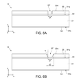
FIG. 5A , thethird wafer 8 is provided, including asubstrate 31, for example having a thickness of approximately between 400 and 800 μm, in particular approximately 600 μm. Thesubstrate 31 is made, according to an embodiment of the present disclosure, of semiconductor material, such as silicon. Thesubstrate 31 has afirst surface 31 a and asecond surface 31 b, opposite to one another in a direction Z. Formed on thefirst surface 31 a by thermal oxidation is afirst interface layer 33, of silicon oxide (SiO2). The step of thermal oxidation typically entails formation of anoxide layer 34 also on the back of thesubstrate 31, on thesecond surface 31 b. The first interface layer 33 (and, likewise, the back oxide layer 34) has, for example, a thickness of approximately between 0.2 μm and 2 μm. - According to a further embodiment of the present disclosure, illustrated in
FIG. 5B , it is possible to form on the interface layer 33 (or as an alternative thereto) one or more furtheranti-wettability layers 33′, which have hydrophobic characteristics, i.e., are designed to provide anti-wettability functions for thenozzle 13 subsequently obtained. These layers are made of materials typically formed by silicon, in compounds containing hydrogen or carbon or fluorine, for example, SixHx, SiC, SiOC. - Formed on the first interface layer 33 (or on the one or more further anti-wettability layers, if present) is a
nozzle layer 35, may, for example, of epitaxially grown polysilicon, having a thickness of approximately between 10 and 75 μm. - The
nozzle layer 35 may be made of a material other than the polysilicon, for example silicon or some other material still, provided that it may be removed selectively with respect to the material of which the first interface layer 33 (or the anti-wettability layer, if present) is formed. - With reference to
FIG. 6A , a photoresist mask (not illustrated) is deposited on an exposedtop surface 35 a of thenozzle layer 35 and, by subsequent lithographic and etching steps, a throughhole 35′ is formed through thenozzle layer 35, until a surface region of theinterface layer 33 is exposed. In the case where one or more furtheranti-wettability layers 33′ are present on theinterface layer 33, said further layers are etched and removed in this process step so as to be self-aligned during complete opening of the nozzle. - Etching is carried out using an etching chemistry capable of selectively removing the material of which the
nozzle layer 35 is made (here, polysilicon), but not the material of which theinterface layer 33 is made (here, silicon oxide). The profile of etching of theintermediate layer 35 may be controlled by choosing an etching technology and an etching chemistry in order to obtain the desired result. - For instance, with reference to
FIG. 6A , using an etch of a dry type (RIE or DRIE) with standard silicon-etching chemistries used in the semiconductor industry (SF6, HBr, etc.) it is possible to obtain a throughhole 35′ with substantially vertical side walls along Z. The throughhole 35′ forms the ejection nozzle of the fluid-ejection device 1. However, as described more fully with reference toFIG. 7 , subsequent manufacturing steps envisage formation of a covering layer (reference number 42 inFIG. 7 ) on the inner walls of the throughhole 35′, which thus causes a narrowing thereof. - The
covering layer 42 is, in particular, a layer presenting good characteristics of wettability, for example a layer of silicon oxide (SiO2). Thecovering layer 42 is considered to have good characteristics of wettability when it presents a reduced angle of contact with a drop of liquid (typically, a water-based liquid or inks of different fluids) deposited thereon. The solid-liquid interaction, as is known, may be assessed in terms of angle of contact of a drop of fluid deposited on the surface considered, measured as angle formed at the surface-liquid interface. A small angle of contact is due to the tendency of the drop to flatten out on the surface, and vice versa. In general, a surface is considered hydrophilic when it presents characteristics of wettability such that, when a drop is deposited thereon, the angle of contact between the surface and the drop (angle θ) has a value of less than 90°, in particular equal to or less than approximately 20° (this facilitates expulsion of any possible air bubble trapped within the chamber displacing it from the walls). A surface is, instead, considered as hydrophobic if it presents characteristics of wettability such that, when a drop is deposited thereon, the angle of contact between the surface and the drop (angle θ) has a value greater than 90°. - Consequently, assuming a through
hole 35′ of a circular shape, in top plan view, the diameter d1 thereof is chosen larger than the desired diameter for the ejection nozzle, as a function of the thickness envisaged for the covering layer of the inner walls of the throughhole 35′. - Alternatively, as illustrated in
FIG. 6B , using an etch of a dry type (with the etching chemistries referred to above) or a wet type (with TMAH or KOH etching chemistry) it is possible to obtain a throughhole 35″ with inclined side walls, which extend, in particular, in lateral sectional view, with an angle a of from 0° to 37° with respect to the direction Z. InFIG. 6B , the throughhole 35″ has a top base opening (at thetop surface 35 a of the nozzle layer 35) of a circular shape and with a diameter d2 larger than the diameter d1 of the bottom base opening (through which theinterface layer 33 is exposed); i.e., it extends in the form of a conical frustum. Also in this case, since subsequent manufacturing steps envisage formation of the covering layer (reference number 42 inFIG. 7 ) on the inner walls of the throughhole 35″, the base diameters d1 and d2 are small. Consequently, assuming a throughhole 35″ having a circular shape in top plan view, the base diameters d1 and d2 thereof are chosen larger than the desired value for the ejection nozzle, as a function of the thickness envisaged for the covering layer of the inner walls of the throughhole 35″. - The step of formation of the through
hole 35′ or 35″, according to the respective embodiments, is followed by the step of removal of the photoresist mask and, if desired, by a step of cleaning of thetop surface 35 a of thenozzle layer 35 and of the side walls internal to the throughhole 35′, 35″. This step, carried out by removal in oxidizing environments at a high temperature (>250° C.) and/or in aggressive solvents, has the function of removing undesired polymeric layers that may form during the previous etching step. - In what follows, a through
hole 35′ of the type illustrated inFIG. 6A will be described, without this implying any loss of generality. What has been described, in fact, applies without significant variations also to the wafer machined as illustrated inFIG. 6B . - With reference to
FIG. 7 , an optional step of thermal oxidation of thewafer 8 is carried out, for example at a temperature comprised between 800° C. and 1100° C., to form a thermal-oxide layer 38 on thenozzle layer 35. This step has the function of enabling formation of the thin thermal-oxide layer 38 presenting a low surface roughness. Instead of by thermal oxidation, the aforesaid oxide may be deposited, totally or in part, for example with techniques of a CVD type. - The
oxide layer 42 extends on the top face of thewafer 8 and within the throughhole 35′, coating the side walls thereof. The thickness of theoxide layer 42 is comprised between 0.2 μm and 2 μm. - The diameter d3 of the through
hole 35′ resulting after the step of formation of theoxide layer 42 has a value comprised between 1 μm and 100 μm, for example equal to 20 μm. - With reference to
FIG. 8 , formed on theoxide layer 42 is astructural layer 45, for example of polysilicon. Thestructural layer 45 has a final thickness comprised between 5 μm and 200 μm, for example 100 μm. Thestructural layer 45 is, for instance, grown epitaxially on theoxide layer 42 and within the throughhole 35′, until a thickness greater than the desired thickness is reached (for example, approximately 3-5 μm more), and is then subjected to a step of CMP to reduce the thickness thereof and obtain an exposed top surface with low roughness. - This is followed by formation of a
second portion 10″ of thechamber 10 and removal of the polysilicon that, in the previous step, has filled the throughhole 35′. For this purpose, anetching mask 50 is provided on the structural layer, and an etching step (identified by the arrows 51) is carried out in the region where the throughhole 35′ had previously been formed. Etching is carried out with an etching chemistry designed to remove the polysilicon of which thestructural layer 45 is made, but not the silicon oxide of thelayer 42. Etching proceeds up to complete removal of the polysilicon that extends within the throughhole 35′ to form thesecond portion 10″ of thechamber 10 through thestructural layer 45 in fluid communication with the through opening 35′, as illustrated inFIG. 9 . - The thickness of the
structural layer 45 defines the volume of thesecond portion 10″ of thechamber 10. According to one aspect of the present disclosure, the volume defined by thesecond portion 10″ is comprised between 90% and the 40% of the total volume designed for thechamber 10, and more in particular between 90% and 80% (as a function of the volume of thefirst portion 10′ discussed previously). - As illustrated in
FIG. 10 , the stack formed by the first andsecond wafers third wafer 8 via the wafer-to-wafer bonding technique using adhesive materials for thebonding 15, which may, for example, be polymeric, or else metallic, or else vitreous. - In particular, the
third wafer 8 is coupled to thefirst wafer 2 so that the first andsecond portions 10′, 10″ concur in forming a single fluid-containment chamber, i.e., thechamber 10. - With reference to
FIG. 11 theoxide layer 34 and thesubstrate 31 is removed. This step may be carried out by grinding theoxide layer 34 and part of thesubstrate 31, or else by a chemical etch, or else by a combination of these two processes. - According to the embodiment of
FIG. 12 , thelayer 33 is removed only at the top surface of the layer 35 (in the plane XY), and not along the inner walls of the nozzle 13 (for example, using an etching technique of a dry type, with an etching chemistry that is standard in semiconductor technologies). - According to one aspect of the present disclosure, the
layer 33 is removed on thelayer 35 only at the ink-outlet nozzles. - What has been described applies, in a similar way, also in the case where on the oxide layer 33 (or as an alternative thereto) one or more further anti-wettability layers were present. In this case, however, the step of removal of the
structural layer nozzle 13 in the case where it were present. - Once again with reference to
FIG. 12 , formation of theinlet channel 9 is then completed by completely removing thestructural layers second wafer 4. - A step of partial sawing of just the
second wafer 4, along thescribe line 57 illustrated inFIG. 12 , enables removal of an edge portion thereof in a region corresponding to theconductive pads 21, so as to render them accessible from outside for a subsequent wire-bonding operation. The fluid-ejection device ofFIG. 1 is thus obtained. -
FIGS. 13-15 show the liquid-ejection device 1 in operating steps, during use. - In a first step (
FIG. 13 ), thechamber 10 is filled by afluid 6 that is to be ejected. This step of loading of thefluid 6 is carried out through theinlet channel 9. - With reference to
FIG. 14 , thepiezoelectric actuator 3 is governed through the top andbottom electrodes 18, 19 (which are biased by theconductive paths 23, 25) so as to generate a deflection of themembrane 7 towards the inside of thechamber 10. This deflection causes a movement of thefluid 6, which, from thechamber 10, passes directly (i.e., without intermediate channels) in thenozzle 13, with consequent controlled ejection of a drop offluid 6 towards the outside of the fluid-ejection device 1. - With reference to
FIG. 15 , thepiezoelectric actuator 3 is governed through the top andbottom electrodes membrane 7 in a direction opposite to the one illustrated inFIG. 14 so as to increase the volume of thechamber 10, further recallingfluid 6 towards thechamber 10 through theinlet channel 9. Thechamber 10 is thus recharged withfluid 6. It is thus possible to proceed cyclically by operating thepiezoelectric actuator 3 for ejection of further drops of fluid. The steps ofFIGS. 14 and 15 are then repeated throughout the printing process. - Operation of the piezoelectric element by biasing of the top and
bottom electrodes - From an examination of the characteristics of the disclosure provided herein, the advantages that it affords are evident.
- In particular, the direct fluidic connection between the
chamber 10 and thenozzle 13 enables optimization of the resonance frequency of the print head in all the operating conditions, and likewise enables an increase in the velocity of ejection of fluid from thenozzle 13. - Furthermore, the steps of production of the nozzle are carried out on the
third wafer 8 prior to coupling of the latter to thefirst wafer 2. This makes possible the use of a wide range of micromachining technologies without running the risk of damaging the coupling layers between the first and thethird wafers nozzle 13 in a simple and inexpensive way. - Further, it should be noted that the steps of production of the liquid-ejection device specify coupling of just three wafers, thus reducing the risks of misalignment in so far as just two steps of coupling of wafers are desired, thus limiting the manufacturing costs.
- With reference to
FIG. 16A , the liquid-ejection device 1 a shown is the same stage of manufacture as the liquid-ejection device 1 ofFIG. 12 except that the liquid-ejection device la includes a further processing step. In particular, the manufacturing of the liquid-ejection device la includes forming a throughhole 49 in thesubstrate 22 to thechamber 5. Thechamber 5 walls, which may include thepiezoelectric actuator 3, are then coated with an insulative material. In particular, the chamber walls, and possibly thepiezoelectric actuator 3, are coated by introducing an atomic layer deposition (ALD) of alayer hafnium dioxide 50 through the throughhole 49. The layer ofhafnium dioxide 50 provides a barrier against humidity. Upon forming the layer ofhafnium dioxide 50, the throughhole 49 may then be closed by known methods. - With reference to
FIG. 16B , the liquid-ejection device 1 b shows a similar stage of manufacture as the liquid-ejection device la ofFIG. 16A , except that the liquid-ejection device 1 b includes yet a further processing step. In particular, the manufacturing of the liquid-ejection device 1 b includes coating more layers of the device, such as surfaces of thechamber 10, thetrench 9, and thenozzle 13 with the insulative layer, such as by ALD of a layer ofhafnium dioxide 50. Furthermore, the layer of hafnium dioxide may be located on outer layers of the liquid-ejection device 1 b, such as on an outer layer ofsubstrate 22. The layer of hafnium dioxide protects the surfaces, such as surfaces of the chamber and the conduits, such as thetrench 9 and thenozzle 13, against corrosive inks to be used with the device. - Finally, it is clear that modifications and variations may be made to what has been described and illustrated herein, without thereby departing from the scope of the present disclosure.
- In particular, as illustrated in the figures, the present disclosure applies, in a per se known manner to the person skilled in of the art on the basis of what has been set forth above, also to fluid-ejection devices that have, in addition to the inlet hole or
channel 9, a further recirculation hole or channel, coupled to the fluid-containment chamber 10 to enable recirculation of thefluid 6 not ejected through thenozzle 13. A fluid-ejection device of this type is described, for example, in the U.S. Pat. No. 9,744,765. - The various embodiments described above can be combined to provide further embodiments. These and other changes can be made to the embodiments in light of the above-detailed description. In general, in the following claims, the terms used should not be construed to limit the claims to the specific embodiments disclosed in the specification and the claims, but should be construed to include all possible embodiments along with the full scope of equivalents to which such claims are entitled. Accordingly, the claims are not limited by the disclosure.
Claims (23)
Priority Applications (1)
| Application Number | Priority Date | Filing Date | Title |
|---|---|---|---|
| US17/107,683 US11498335B2 (en) | 2018-01-17 | 2020-11-30 | Method for manufacturing a fluid-ejection device with improved resonance frequency and fluid ejection velocity, and fluid-ejection device |
Applications Claiming Priority (2)
| Application Number | Priority Date | Filing Date | Title |
|---|---|---|---|
| IT201800001152A IT201800001152A1 (en) | 2018-01-17 | 2018-01-17 | MANUFACTURING METHOD OF A FLUID EJECTION DEVICE WITH IMPROVED RESONANCE FREQUENCY AND FLUID EJECTION SPEED, AND FLUID EJECTION DEVICE |
| IT102018000001152 | 2018-01-17 |
Related Child Applications (1)
| Application Number | Title | Priority Date | Filing Date |
|---|---|---|---|
| US17/107,683 Division US11498335B2 (en) | 2018-01-17 | 2020-11-30 | Method for manufacturing a fluid-ejection device with improved resonance frequency and fluid ejection velocity, and fluid-ejection device |
Publications (2)
| Publication Number | Publication Date |
|---|---|
| US20190217618A1 true US20190217618A1 (en) | 2019-07-18 |
| US10875307B2 US10875307B2 (en) | 2020-12-29 |
Family
ID=61873844
Family Applications (2)
| Application Number | Title | Priority Date | Filing Date |
|---|---|---|---|
| US16/249,752 Active US10875307B2 (en) | 2018-01-17 | 2019-01-16 | Method for manufacturing a fluid-ejection device with improved resonance frequency and fluid-ejection velocity, and fluid-ejection device |
| US17/107,683 Active US11498335B2 (en) | 2018-01-17 | 2020-11-30 | Method for manufacturing a fluid-ejection device with improved resonance frequency and fluid ejection velocity, and fluid-ejection device |
Family Applications After (1)
| Application Number | Title | Priority Date | Filing Date |
|---|---|---|---|
| US17/107,683 Active US11498335B2 (en) | 2018-01-17 | 2020-11-30 | Method for manufacturing a fluid-ejection device with improved resonance frequency and fluid ejection velocity, and fluid-ejection device |
Country Status (3)
| Country | Link |
|---|---|
| US (2) | US10875307B2 (en) |
| CN (2) | CN210082663U (en) |
| IT (1) | IT201800001152A1 (en) |
Cited By (3)
| Publication number | Priority date | Publication date | Assignee | Title |
|---|---|---|---|---|
| JP2021020388A (en) * | 2019-07-29 | 2021-02-18 | キヤノン株式会社 | Manufacturing method of substrate joined body, substrate for liquid discharge head, and manufacturing method of substrate for liquid discharge head |
| WO2021188098A1 (en) * | 2020-03-17 | 2021-09-23 | Hewlett-Packard Development Company, L.P. | Fluid ejection head fluid coating |
| JP7476742B2 (en) | 2020-09-24 | 2024-05-01 | ブラザー工業株式会社 | Liquid ejection head |
Families Citing this family (3)
| Publication number | Priority date | Publication date | Assignee | Title |
|---|---|---|---|---|
| IT201800001152A1 (en) | 2018-01-17 | 2019-07-17 | St Microelectronics Srl | MANUFACTURING METHOD OF A FLUID EJECTION DEVICE WITH IMPROVED RESONANCE FREQUENCY AND FLUID EJECTION SPEED, AND FLUID EJECTION DEVICE |
| IT201900007213A1 (en) * | 2019-05-24 | 2020-11-24 | St Microelectronics Srl | METHOD OF MANUFACTURING A STACKED PIEZOELECTRIC TRANSDUCER AND PIEZOELECTRIC TRANSDUCER |
| JP2025024850A (en) * | 2023-08-08 | 2025-02-21 | キヤノン株式会社 | ACTUATOR, ELEMENT SUBSTRATE AND LIQUID EJECTION HEAD |
Citations (3)
| Publication number | Priority date | Publication date | Assignee | Title |
|---|---|---|---|---|
| US8864287B2 (en) * | 2011-04-19 | 2014-10-21 | Eastman Kodak Company | Fluid ejection using MEMS composite transducer |
| US8944573B2 (en) * | 2012-02-27 | 2015-02-03 | Toshiba Tec Kabushiki Kaisha | Inkjet head and method of manufacturing the same |
| US20170182778A1 (en) * | 2015-12-29 | 2017-06-29 | Stmicroelectronics S.R.L. | Manufacturing method for a fluid-ejection device, and fluid-ejection device |
Family Cites Families (7)
| Publication number | Priority date | Publication date | Assignee | Title |
|---|---|---|---|---|
| JP2009190349A (en) * | 2008-02-18 | 2009-08-27 | Seiko Epson Corp | Method for manufacturing liquid jet head |
| US8633553B2 (en) | 2010-07-26 | 2014-01-21 | Stmicroelectronics S.R.L. | Process for manufacturing a micromechanical structure having a buried area provided with a filter |
| JP2013538446A (en) * | 2010-07-26 | 2013-10-10 | 富士フイルム株式会社 | Formation of devices with curved piezoelectric films |
| ITTO20120426A1 (en) * | 2012-05-11 | 2013-11-12 | St Microelectronics Srl | PROCESS OF MANUFACTURING A NOZZLE PLATE, NOZZLE PLATE, AND LIQUID EJECTION DEVICE EQUIPPED WITH NOZZLE PLATE |
| ITTO20130312A1 (en) | 2013-04-18 | 2014-10-19 | St Microelectronics Srl | METHOD OF MANUFACTURE OF A FLUID EJECTION DEVICE AND FLUID EJECTION DEVICE |
| ITUB20156035A1 (en) | 2015-11-30 | 2017-05-30 | St Microelectronics Srl | FLUID EJECTION DEVICE WITH RESTRING CLOG, AND METHOD OF MANUFACTURE OF THE SAME |
| IT201800001152A1 (en) * | 2018-01-17 | 2019-07-17 | St Microelectronics Srl | MANUFACTURING METHOD OF A FLUID EJECTION DEVICE WITH IMPROVED RESONANCE FREQUENCY AND FLUID EJECTION SPEED, AND FLUID EJECTION DEVICE |
-
2018
- 2018-01-17 IT IT201800001152A patent/IT201800001152A1/en unknown
-
2019
- 2019-01-16 US US16/249,752 patent/US10875307B2/en active Active
- 2019-01-16 CN CN201920070358.XU patent/CN210082663U/en not_active Withdrawn - After Issue
- 2019-01-16 CN CN201910040227.1A patent/CN110039899B/en active Active
-
2020
- 2020-11-30 US US17/107,683 patent/US11498335B2/en active Active
Patent Citations (3)
| Publication number | Priority date | Publication date | Assignee | Title |
|---|---|---|---|---|
| US8864287B2 (en) * | 2011-04-19 | 2014-10-21 | Eastman Kodak Company | Fluid ejection using MEMS composite transducer |
| US8944573B2 (en) * | 2012-02-27 | 2015-02-03 | Toshiba Tec Kabushiki Kaisha | Inkjet head and method of manufacturing the same |
| US20170182778A1 (en) * | 2015-12-29 | 2017-06-29 | Stmicroelectronics S.R.L. | Manufacturing method for a fluid-ejection device, and fluid-ejection device |
Cited By (4)
| Publication number | Priority date | Publication date | Assignee | Title |
|---|---|---|---|---|
| JP2021020388A (en) * | 2019-07-29 | 2021-02-18 | キヤノン株式会社 | Manufacturing method of substrate joined body, substrate for liquid discharge head, and manufacturing method of substrate for liquid discharge head |
| JP7346131B2 (en) | 2019-07-29 | 2023-09-19 | キヤノン株式会社 | Method for manufacturing substrate assembly, substrate for liquid ejection head, and method for manufacturing substrate for liquid ejection head |
| WO2021188098A1 (en) * | 2020-03-17 | 2021-09-23 | Hewlett-Packard Development Company, L.P. | Fluid ejection head fluid coating |
| JP7476742B2 (en) | 2020-09-24 | 2024-05-01 | ブラザー工業株式会社 | Liquid ejection head |
Also Published As
| Publication number | Publication date |
|---|---|
| US20210078331A1 (en) | 2021-03-18 |
| CN110039899A (en) | 2019-07-23 |
| US11498335B2 (en) | 2022-11-15 |
| CN210082663U (en) | 2020-02-18 |
| IT201800001152A1 (en) | 2019-07-17 |
| US10875307B2 (en) | 2020-12-29 |
| CN110039899B (en) | 2021-02-05 |
Similar Documents
| Publication | Publication Date | Title |
|---|---|---|
| US10245834B2 (en) | Manufacturing method for a fluid-ejection device, and fluid-ejection device | |
| US11498335B2 (en) | Method for manufacturing a fluid-ejection device with improved resonance frequency and fluid ejection velocity, and fluid-ejection device | |
| US8998388B2 (en) | Method for manufacturing a fluid ejection device and fluid ejection device | |
| US9744765B2 (en) | Fluid ejection device with restriction channel, and manufacturing method thereof | |
| CN108656747B (en) | Fluid ejection device, printhead, printer, and method for making an ejection device | |
| US10946653B2 (en) | Fluid ejection microfluidic device, in particular for ink printing, and manufacturing process thereof | |
| CN109278407A (en) | With piezoelectric actuated microfluid MEMS device and its manufacturing process | |
| US20130083126A1 (en) | Liquid ejection device with planarized nozzle plate | |
| US11884071B2 (en) | Fluid ejection device with reduced number of components, and method for manufacturing the fluid ejection device | |
| JP7309358B2 (en) | LIQUID EJECTION HEAD AND MANUFACTURING METHOD THEREOF | |
| CN103252997A (en) | Liquid spray head and manufacturing method thereof | |
| US8037605B2 (en) | Piezoelectric inkjet printhead and method of manufacturing the same | |
| US20220410183A1 (en) | Microfluidic device for spraying very small drops of liquids | |
| CN102950897B (en) | Liquid nozzle and manufacturing method thereof | |
| US20070134928A1 (en) | Silicon wet etching method using parylene mask and method of manufacturing nozzle plate of inkjet printhead using the same | |
| US20130082028A1 (en) | Forming a planar film over microfluidic device openings |
Legal Events
| Date | Code | Title | Description |
|---|---|---|---|
| AS | Assignment |
Owner name: STMICROELECTRONICS S.R.L., ITALY Free format text: ASSIGNMENT OF ASSIGNORS INTEREST;ASSIGNORS:GIUSTI, DOMENICO;FERRERA, MARCO;PRELINI, CARLO LUIGI;AND OTHERS;SIGNING DATES FROM 20190107 TO 20190108;REEL/FRAME:048038/0620 |
|
| FEPP | Fee payment procedure |
Free format text: ENTITY STATUS SET TO UNDISCOUNTED (ORIGINAL EVENT CODE: BIG.); ENTITY STATUS OF PATENT OWNER: LARGE ENTITY |
|
| STPP | Information on status: patent application and granting procedure in general |
Free format text: DOCKETED NEW CASE - READY FOR EXAMINATION |
|
| STPP | Information on status: patent application and granting procedure in general |
Free format text: NON FINAL ACTION MAILED |
|
| STPP | Information on status: patent application and granting procedure in general |
Free format text: NOTICE OF ALLOWANCE MAILED -- APPLICATION RECEIVED IN OFFICE OF PUBLICATIONS |
|
| STCF | Information on status: patent grant |
Free format text: PATENTED CASE |
|
| MAFP | Maintenance fee payment |
Free format text: PAYMENT OF MAINTENANCE FEE, 4TH YEAR, LARGE ENTITY (ORIGINAL EVENT CODE: M1551); ENTITY STATUS OF PATENT OWNER: LARGE ENTITY Year of fee payment: 4 |