US20190086471A1 - Techniques and circuits for on-chip jitter and phase noise measurement in a digital test environment - Google Patents
Techniques and circuits for on-chip jitter and phase noise measurement in a digital test environment Download PDFInfo
- Publication number
- US20190086471A1 US20190086471A1 US15/708,924 US201715708924A US2019086471A1 US 20190086471 A1 US20190086471 A1 US 20190086471A1 US 201715708924 A US201715708924 A US 201715708924A US 2019086471 A1 US2019086471 A1 US 2019086471A1
- Authority
- US
- United States
- Prior art keywords
- circuit
- phase
- jitter
- output
- digital
- Prior art date
- Legal status (The legal status is an assumption and is not a legal conclusion. Google has not performed a legal analysis and makes no representation as to the accuracy of the status listed.)
- Granted
Links
- 238000012360 testing method Methods 0.000 title claims abstract description 63
- 238000005259 measurement Methods 0.000 title claims description 59
- 238000000034 method Methods 0.000 title claims description 18
- 238000004519 manufacturing process Methods 0.000 claims description 24
- 238000012512 characterization method Methods 0.000 claims description 9
- 230000003595 spectral effect Effects 0.000 claims description 4
- 230000003213 activating effect Effects 0.000 claims description 3
- 238000005070 sampling Methods 0.000 claims description 3
- 230000003111 delayed effect Effects 0.000 claims 2
- 238000000691 measurement method Methods 0.000 abstract description 3
- 235000012431 wafers Nutrition 0.000 description 67
- 230000005540 biological transmission Effects 0.000 description 9
- 238000010586 diagram Methods 0.000 description 7
- 230000001960 triggered effect Effects 0.000 description 6
- 238000004891 communication Methods 0.000 description 5
- 238000005516 engineering process Methods 0.000 description 5
- 238000001228 spectrum Methods 0.000 description 4
- 239000003990 capacitor Substances 0.000 description 3
- 238000012797 qualification Methods 0.000 description 3
- 238000011144 upstream manufacturing Methods 0.000 description 3
- VYPSYNLAJGMNEJ-UHFFFAOYSA-N Silicium dioxide Chemical compound O=[Si]=O VYPSYNLAJGMNEJ-UHFFFAOYSA-N 0.000 description 2
- 238000003491 array Methods 0.000 description 2
- 238000012544 monitoring process Methods 0.000 description 2
- 230000000630 rising effect Effects 0.000 description 2
- 229910052681 coesite Inorganic materials 0.000 description 1
- 239000004020 conductor Substances 0.000 description 1
- 238000011109 contamination Methods 0.000 description 1
- 229910052906 cristobalite Inorganic materials 0.000 description 1
- 230000002950 deficient Effects 0.000 description 1
- 239000011521 glass Substances 0.000 description 1
- 238000003780 insertion Methods 0.000 description 1
- 230000010354 integration Effects 0.000 description 1
- 230000007774 longterm Effects 0.000 description 1
- 230000003287 optical effect Effects 0.000 description 1
- 238000002161 passivation Methods 0.000 description 1
- 239000000377 silicon dioxide Substances 0.000 description 1
- 235000012239 silicon dioxide Nutrition 0.000 description 1
- 229910052682 stishovite Inorganic materials 0.000 description 1
- 238000012546 transfer Methods 0.000 description 1
- 229910052905 tridymite Inorganic materials 0.000 description 1
- 238000013024 troubleshooting Methods 0.000 description 1
Images


Classifications
-
- G—PHYSICS
- G01—MEASURING; TESTING
- G01R—MEASURING ELECTRIC VARIABLES; MEASURING MAGNETIC VARIABLES
- G01R31/00—Arrangements for testing electric properties; Arrangements for locating electric faults; Arrangements for electrical testing characterised by what is being tested not provided for elsewhere
- G01R31/28—Testing of electronic circuits, e.g. by signal tracer
- G01R31/317—Testing of digital circuits
- G01R31/31708—Analysis of signal quality
- G01R31/31709—Jitter measurements; Jitter generators
-
- H—ELECTRICITY
- H03—ELECTRONIC CIRCUITRY
- H03L—AUTOMATIC CONTROL, STARTING, SYNCHRONISATION OR STABILISATION OF GENERATORS OF ELECTRONIC OSCILLATIONS OR PULSES
- H03L7/00—Automatic control of frequency or phase; Synchronisation
- H03L7/06—Automatic control of frequency or phase; Synchronisation using a reference signal applied to a frequency- or phase-locked loop
- H03L7/08—Details of the phase-locked loop
- H03L7/081—Details of the phase-locked loop provided with an additional controlled phase shifter
- H03L7/0812—Details of the phase-locked loop provided with an additional controlled phase shifter and where no voltage or current controlled oscillator is used
- H03L7/0814—Details of the phase-locked loop provided with an additional controlled phase shifter and where no voltage or current controlled oscillator is used the phase shifting device being digitally controlled
-
- H—ELECTRICITY
- H03—ELECTRONIC CIRCUITRY
- H03L—AUTOMATIC CONTROL, STARTING, SYNCHRONISATION OR STABILISATION OF GENERATORS OF ELECTRONIC OSCILLATIONS OR PULSES
- H03L7/00—Automatic control of frequency or phase; Synchronisation
- H03L7/06—Automatic control of frequency or phase; Synchronisation using a reference signal applied to a frequency- or phase-locked loop
- H03L7/08—Details of the phase-locked loop
- H03L7/085—Details of the phase-locked loop concerning mainly the frequency- or phase-detection arrangement including the filtering or amplification of its output signal
- H03L7/089—Details of the phase-locked loop concerning mainly the frequency- or phase-detection arrangement including the filtering or amplification of its output signal the phase or frequency detector generating up-down pulses
-
- H01L27/092—
-
- H—ELECTRICITY
- H10—SEMICONDUCTOR DEVICES; ELECTRIC SOLID-STATE DEVICES NOT OTHERWISE PROVIDED FOR
- H10D—INORGANIC ELECTRIC SEMICONDUCTOR DEVICES
- H10D84/00—Integrated devices formed in or on semiconductor substrates that comprise only semiconducting layers, e.g. on Si wafers or on GaAs-on-Si wafers
- H10D84/80—Integrated devices formed in or on semiconductor substrates that comprise only semiconducting layers, e.g. on Si wafers or on GaAs-on-Si wafers characterised by the integration of at least one component covered by groups H10D12/00 or H10D30/00, e.g. integration of IGFETs
- H10D84/82—Integrated devices formed in or on semiconductor substrates that comprise only semiconducting layers, e.g. on Si wafers or on GaAs-on-Si wafers characterised by the integration of at least one component covered by groups H10D12/00 or H10D30/00, e.g. integration of IGFETs of only field-effect components
- H10D84/83—Integrated devices formed in or on semiconductor substrates that comprise only semiconducting layers, e.g. on Si wafers or on GaAs-on-Si wafers characterised by the integration of at least one component covered by groups H10D12/00 or H10D30/00, e.g. integration of IGFETs of only field-effect components of only insulated-gate FETs [IGFET]
- H10D84/85—Complementary IGFETs, e.g. CMOS
Definitions
- the proposed solution relates to jitter and phase noise characterization, and in particular to systems, circuits and techniques for on-chip jitter and phase noise measurement in a digital test environment.
- TDCs Time-to-Digital Converters
- high resolution jitter and phase noise measurement techniques and circuits having a resolution comparable to what is achievable with a spectrum analyzer but suitable for a digital test environment, particularly suitable, but not limited, to production testing.
- such measurement is enabled to be performed on-chip using a digital Delay Locked Loop (DLL) having a high gain 1-bit phase comparator combined with a digital accumulator and a fine resolution digitally controlled delay element to determine phase differences between the device under test and a reference clock.
- the digitally controlled delay element has a range as large as the max peak-to-peak jitter to be measured for the device under test.
- fine resolution one means controllable down to one part in a hundred or better within the maximum peak-to-pick jitter range of the device under test.
- test chips are provided for production level jitter and phase noise measurements in digital test environments.
- test jigs such as device interface boards, are provided to characterize jitter and phase noise of integrated circuit devices, electronic components incorporating devices to be tested, systems incorporating devices, etc.
- the proposed on-chip jitter and phase noise characterization circuits are employed at run-time, that is during the operation of final products or systems, to provide jitter and phase noise measurement in digital test environments.
- a digital jitter and phase noise measurement circuit comprising a combination of: a high-gain 1-bit phase detector configured to a receive reference clock signal and a feedback signal to provide a phase detector signal; a digital accumulator configured to receive the phase detector signal and output a digital jitter code; and a digitally controlled delay element configured to track an accumulated phase difference between the reference clock signal and a signal output by a device under test such that the output of the digitally controlled delay element provides the feedback signal, said combination providing a digitally controlled delay locked loop having a resolution and range selected to track a phase error between an output signal of the tested device and the reference clock.
- a method of using a digital jitter and phase noise measurement circuit for characterizing the jitter and phase noise of the device comprising a combination of: a high-gain 1-bit phase detector configured to a receive reference clock signal and a feedback signal to provide a phase detector signal; a digital accumulator configured to receive the phase detector signal and output a digital jitter code; and a digitally controlled delay element configured to track an accumulated phase difference between the reference clock signal and a signal output by a device under test such that the output of the digitally controlled delay element provides the feedback signal, said combination providing a digitally controlled delay locked loop having a resolution and range selected to track a phase error between an output signal of the tested device and the reference clock.
- a method for characterizing the jitter and phase noise of a device comprising: providing a high-gain 1-bit phase detector configured to a receive reference clock signal and a feedback signal to provide a phase detector signal; providing a digital accumulator configured to receive the phase detector signal and output a digital jitter code; and providing a digitally controlled delay element configured to track an accumulated phase difference between the reference clock signal and a signal output by a device under test such that the output of the digitally controlled delay element provides the feedback signal, the combination providing a digitally controlled delay locked loop having a resolution and range selected to track a phase error between an output signal of the tested device and the reference clock.
- FIG. 1 is schematic plot showing simulated phase noise variability for low node FinFet technology
- FIG. 2A is a schematic circuit diagram illustrating a circuit schematic in accordance with an embodiment of the proposed solution
- FIG. 2B is a schematic circuit diagram illustrating a realization of a high gain linear digital phase detector employing delay transmission lines in accordance with an implementation of the proposed solution
- FIG. 2C is a schematic circuit diagram illustrating another realization of a high gain linear digital phase detector employing integrators in accordance with another implementation of the proposed solution
- FIGS. 3A and 3B are schematic plots illustrating representations of experimental measurements in accordance with an implementation of the proposed solution
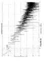
- FIG. 3C is a schematic plot illustrating a representation of power spectral density of the phase error corresponding to measurements illustrated in FIG. 3A and 3B in accordance with the implementation of the proposed solution;
- FIGS. 4A and 4B are schematic diagrams illustrating jitter and phase noise measurement circuits wafer-level manufactured on the same wafer with devices to be characterized in accordance with various embodiments of the proposed solution;
- FIGS. 5A and 5B are schematic diagrams illustrating jitter and phase noise measurement circuits wafer-level manufactured on a separate wafer from devices wafer-level manufactured on other wafers to be tested in accordance with another embodiment of the proposed solution, the combination of FIGS. 5A and 5B illustrating flip-chip testing in accordance with some device characterization procedures proposed herein;
- FIGS. 6A and 6B are schematic diagrams illustrating electronic components employing the jitter and phase noise measurement circuits of the proposed solution in various digital test environments in accordance with different embodiments thereof.
- FIG. 7 is schematic diagram illustrating a digital test environment in accordance with an embodiment of the proposed solution.
- VCO Voltage Controlled Oscillator
- LC Inductance-Capacitance
- FIG. 1 illustrates a plot showing simulated phase noise variability for low node FinFet technology having a larger than 15 dB variation between best and worst case flicker noise model.
- dBc refers to the ratio of power of the noise relative to power in a carrier expressed in decibels.
- the operating principles of proposed digital on-chip jitter and phase noise measurement techniques and circuits include the use of a digitally controlled Delay Locked Loop (DLL) having a very fine resolution but limited range to track the phase error between a tested device output clock and the reference clock input.
- DLL Delay Locked Loop
- Some embodiments employ a combination of a high-gain 1-bit phase detector, a digital accumulator and a fine digitally controlled delay element to track the accumulated phase difference between the reference clock and the output of the device under test. Observing the accumulator output provides an indication of the jitter and performing a Fast Fourier Transform (FFT) of the accumulator output provides the phase noise of the device under test.
- FFT Fast Fourier Transform
- FIG. 2A illustrates, in accordance with an embodiment, such a proposed on-chip jitter and phase noise measurement circuit for characterizing a PLL device in a digital test environment.
- a digital on-chip jitter and phase noise measurement circuit 100 includes a digital delay-locked loop 102 built using a 1-bit high gain digital phase detector 104 followed by an accumulator 106 and a very fine digitally controlled delay element 108 to track the accumulated phase difference between the output clock 110 and the reference clock 112 within the DLL 102 tracking bandwidth.
- the controlled delay element 108 can have a range as large as the peak-to-peak jitter of the device under test to be measured, and a fine resolution controllable down to one part in a hundred or better.
- the ideal output clock signal 110 has an approximately constant signal period, various specific periods throughout the output clock signal 110 train may deviate from the ideal output signal period. This deviation may be the result of PLL error introduced by one or more subcomponents of the PLL device for example resulting in excessive cycle-to-cycle period jitter, long term jitter, phase jitter and other forms of phase noise. These and/or other types of phase noise and associated jitter may be characteristic to other devices under test 120 . Devices under test 120 having least phase noise and jitter can be preferentially selected from others which underperform.
- the high gain digital phase detector 104 determines an amount of PLL error based on the reference clock signal 112 and the feedback output signal.
- the digital phase detector 104 can have a resolution of about ⁇ 20 fs.
- the high gain digital phase detector can include a non-linear bang-bang phase detector which can be realized using an arbiter or strong-arm comparator.
- the high gain digital phase detector can include a linear digital phase detector capable of providing a multi-bit output.
- FIG. 2B illustrates the realization of a high gain linear digital phase detector 104 employing delay transmission lines 422 , 424 .
- Reference clock 112 and feedback signals are employed to clock corresponding flip-flops 402 and 404 which output corresponding step function signals 412 and 414 .
- the Up 412 and Down 414 step function signals are provided to corresponding transmission lines 422 and 424 .
- the clear Up 412 and Down 424 signals are sampled and the feedback signal flip-flop 404 is reset to initialize (following) sampling as is usually done in an overlapping pulse phase detector, for example employing an AND gate 410 .
- Each delay line 422 , 424 includes sample points along thereof with inverters (not shown) between sample points.
- Inverters along the two transmission lines 422 , 424 toggle as a corresponding travelling wave of the step function signal 412 , 414 propagates through each delay line 422 , 424 and passes their location. If the flip-flop 402 is triggered before the flip-flop 404 , then a number of additional inverters that are in turn tripped along the transmission line 422 will be higher than a number of inverters (at least one) that tripped in to the transmission line 424 . Conversely, if the flip-flop 404 is triggered before the flip-flop 402 , then the number of additional inverters that are in turn tripped along the transmission line 424 will be higher than the number of inverters (at least one) that tripped in to the transmission line 422 .
- a one-shot trigger element 420 can be employed to control the lowest number of inverters triggered in a transmission line 422 , 424 .
- the number of inverters triggered in delay line 422 , THREM_UP, and the number of inverters triggered in delay line 424 , THREM_DWN, are compared by comparator 430 when triggered by the output of the trigger element 420 .
- Digital phase signal 116 is output by the comparator 430 .
- THERM_UP and THERM_DWN can be digital thermometer words of a length equal to the number of inverters tripped on the delay line 422 , 424 . This first realization of the linear phase detector implementation has a relatively lower range but likely has a better accuracy.
- FIG. 2C illustrates another realization of a high gain linear digital phase detector 104 employing integrators 442 , 444 . Description of similar elements in FIG. 2B is not repeated.
- the Up and Down step function signals 412 , 414 each trigger the start of corresponding charging processes on preferably identical integrator circuits 442 , 444 that drive current into precharged capacitors (on both sides P and N). Both step function signals 412 and 414 will have substantially identical turn on and turn off characteristics until prior to the sensing non-overlapping pulses phase detector 410 .
- step function signals 412 and 414 act identically and a voltage difference across the two capacitors represents linearly the difference in charging pulse length time between the step function signals 412 and 414 .
- the difference in voltage between the capacitors is output by comparator 430 , for example implemented as an offset compensated flash converter. The output provides the digital phase signal 116 .
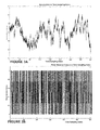
- FIG. 3B illustrates a representation of variability measured at the phase detector output 116 .
- the delay element 108 is a digitally programmable device which includes functionality to adjust the rising edge or falling edge of the feedback signal within a predefined resolution and/or bandwidth range.
- the digitally controlled delay element 108 has a small range of a few ps and a control resolution of about ⁇ 20 fs.
- the digital accumulator code 114 can be used to extract jitter information.
- the digital accumulator 106 may include functionality to produce a digital code signal 114 for operating the digital delay element 108 .
- a digital code signal may include a binary code designating whether the delay element 108 moves the rising edge of the feedback signal. For example, if the digital accumulator 106 produces a code signal with a ‘1’, then the delay element 108 may delay the feedback signal by a specific amount of time. If the code signal is a ‘0’, then the delay element 108 may advance the feedback signal by a specific amount of time.
- the code signal is a multibit code signal ‘100101’ which determines a specific amount of phase delay or an amount of phase advance with finer time steps. For example, performing an FFT of the accumulator output 114 would provide the power spectral density of the phase error produced by the device 120 under test (phase noise).
- a feedback “/N” divider circuit can be employed in the signal path between the output of the tested device 120 (PLL) and the input of the digital delay element 104
- a feedback “/M” divider circuit can be employed in the feedback signal path between the output of the digital delay element 108 and the digital phase detector 104 , or both.
- Each feedback divider can be implemented in hardware, such as in an integrated circuit (rollover counter), that includes functionality to divide the frequency of the output signal 110 or the feedback signal.
- the operating frequency output by the VCO may be a multiple of the reference clock and is reduced by the feedback divider(s) down to the frequency of the reference clock for jitter and phase noise measurement herein.
- FIGS. 3A and 3B illustrate, in accordance with the proposed solution, representations of experimental measurements of digital on-chip jitter.
- FIG. 3A illustrates a representation of variability measured at the accumulator output 114 while
- FIG. 3B illustrates a representation of variability measured at the phase detector output 116 .
- FIG. 3C illustrates a representative FFT.
- clock output 110 of transceiver/modems production tested and selected in accordance with the proposed solution would express a tight jitter and phase noise distribution, performance which would be (strongly) desired.
- Benefits can be derived from implementing the proposed solution at wafer-level manufacture and/or chip-level production. For example, the cost of finding a faulty device goes up by a factor of ten between manufacturing levels (die, packaged chip, board, etc.) Discarding faulty/defective/subpar devices 120 such as, but not limited to: PLLs, VCOs, Digital to Analog Converters (DACs), Serializer/Deserializers (SerDes) (jitter transfer function and jitter mask), having unacceptable jitter as early as possible would lower the overall cost of transceivers, modems, pluggable modules, line cards, etc. incorporating such devices. In other embodiments digital clock trees are characterized with respect to jitter with the intent to discard components having excessive jitter.
- FIG. 4A illustrates an arrangement of multiple wafer-level manufactured devices wafer-level manufactured together with jitter and phase noise measurements circuits.
- Each jitter and phase noise measurement circuit 100 is wafer-level manufactured on the same wafer 252 with a corresponding group of devices 120 to be wafer-level tested.
- Selector/splitter circuitry “S” for selection of each device 120 for characterization is also wafer-level manufactured along with a corresponding jitter and phase noise measurement circuit 100 on the same wafer 252 .
- Each jitter and phase noise measurement circuit 100 is provided with reference clock signal 112 (and can also be configured to output the clock signal 110 from the selected device under test 120 ) via signal traces routed for example to an edge of the wafer 252 .
- Another trace 222 carries a control signal from the edge of the wafer 252 to selector/splitter S corresponding to the jitter and phase noise measurement circuit 100 .
- selector/splitter S can be configured to route the reference clock signal 112 between the jitter and phase noise measurement circuit 100 and the device 120 selected for testing in response to control signal 222 .
- the digital jitter code output 114 from the accumulator ( 106 ) is routed to another pad on the edge of the wafer 252 .
- the wafer edge pads are employed in providing connection upstream to automated test equipment (not illustrated).
- a selection of devices 120 having desired compliant performance can be sectioned off from the jitter and phase noise measurement circuits 100 proposed herein during chip level manufacture of the devices 120 .
- Dashed lines indicate dicing lines for singulating devices 120 out of the wafer 252 after qualification.
- the jitter and phase noise measurement circuits 100 , selector/splitter circuits S and interconnecting traces are wafer-level manufactured on sacrificial portions of the wafer 252 .
- the dotted arrow represents singulation of individual devices 120 . Singulation exposes device connection pads 302 , 304 for each device 120 die. It is understood that only a small group of the illustrated features are labeled solely in order to simplify illustration herein. For example, ground and power traces, and pads are omitted.
- FIG. 4B illustrates another arrangement of multiple wafer-level manufactured devices wafer-level manufactured together with jitter and phase noise measurements circuits.
- Each jitter and phase noise measurement circuit 100 is wafer-level manufactured on the same wafer 254 with a corresponding device 120 .
- Selector (or splitter) circuitry “S” for selection of each device 120 for characterization is also wafer-level manufactured on the same wafer 254 , for example in sacrificial portions of wafer 254 .
- Each jitter and phase noise measurement circuit 100 is provided with reference clock signal 112 (for example when selected via signal 222 ) (and can be configured to output the clock signal 110 from the selected device 120 under test) via signal traces routed, for example, to an edge of the wafer 254 .
- Trace 222 is (a bus) illustrated to carry the control signal from the edge of the wafer 254 to selector/splitter S together with the reference clock signal 112 .
- selector/splitter S routes the clock signal 112 to the selected jitter and phase noise measurement circuit 100 for testing as directed by control signal 222 .
- the digital jitter code output 114 from the accumulator 106 of each jitter and phase noise measurement circuit 100 is routed to corresponding pads on the edge of the wafer 254 .
- the wafer edge pads are employed in providing connection upstream to automated test equipment (not illustrated).
- each device 120 and corresponding jitter and phase noise measurement circuit 100 proposed herein can be sectioned off together during chip level manufacture of the devices 120 .
- Dashed lines indicate dicing lines for singulating dice 122 including a device 120 and its corresponding jitter and phase noise measurement circuit 100 out of the wafer 254 after wafer level characterization.
- the selector/splitter circuit(s) S and interconnecting traces are wafer-level manufactured on sacrificial portions of the wafer 254 .
- the dotted arrow represents singulation of each die 122 including device 120 and its corresponding jitter and phase noise measurement circuit 100 .
- Singlation exposes device connection pads 302 , 304 for each device 120 and digital jitter code output 114 pad on the edges of the die 122 . It is understood that only a small group of the illustrated features are labeled solely in order to simplify illustration herein. For example, ground and power traces and pads are omitted. Without limiting the invention, additional circuitry (not shown) can be wafer-level manufactured on each die 122 to activate/deactivate jitter and phase noise measurement circuit 100 . The combination of the device 120 and jitter and phase noise measurement circuit 100 can be used to characterize and/or qualify intermediate or final components or systems incorporating die 122 during subsequent manufacturing and/or operation of such intermediate or final components or systems.
- FIGS. 5A and 5B illustrate separately manufactured wafers, a wafer 264 including wafer-level manufactured device 120 arrays and another corresponding wafer 262 including wafer-level manufactured jitter and phase noise measurement circuit 100 arrays.
- wafer 262 having multiple jitter and phase noise measurements circuits 100 implements at least a portion of automated test equipment.
- the wafer 262 has an arrangement of pads 202 , 204 (only a few pairs labeled) and selection/splitter circuitry labeled “Selector”.
- Reference clock 112 , output clock 110 and digital jitter code 114 traces can be routed to an edge of the wafer 262 to corresponding pads.
- the wafer edge pads are employed in providing connection upstream to automated test equipment (not illustrated). For example, ground and power traces and pads are omitted.
- the dotted lines schematically represent wafer alignment marks solely for ease of description herein. In practice alignment can be provided via other known flip-chip wafer-level manufacture methods.
- Wafer 264 including devices 120 has an arrangement of pads 302 , 304 corresponding to pads 202 , 204 of wafer 262 . Dashed lines illustrate score lines employed for dicing and/or flip-chip wafer alignment. Multiple device wafers 264 are wafer-level manufactured in batches and each wafer 264 is wafer-level mass characterized (in parallel) in flip-chip fashion by connection to testing wafer 262 . For example, without limiting the invention thereto, arrows indicate left-to-right flipping device wafer 264 and placement of the flipped wafer 264 over on top of testing wafer 262 such that pads 302 , 304 register with pads 202 , 204 .
- testing wafer 262 can be protected from electrical shorts by a passivation layer or SiO2 glass layer, except for pads 202 , 204 which are left exposed. Electrical contact between pads 202 / 302 and 204 / 304 can be provided by employing a conductive material such as a layer of conductive paste. In other implementations (not shown), pads 202 , 204 of the testing wafer 262 make electrical contact with sacrificial (not shown) test connection pads on the wafer 264 different from pads 302 , 304 . For example, such sacrificial test connection pads limit testing damage and/or surface contamination of devices 120 on wafer 264 prior to singulation (dotted arrow).
- Additional benefits can be derived by employing the proposed solution in intermediate and final products, either during manufacture, integration, deployment, provisioning and/or at run-time to provide assessments of the jitter performance of the overall systems in use in real time.
- FIG. 6A illustrates jitter and phase noise measurement in a digital test environment.
- an integrated circuit implementing the jitter and phase noise measurement circuit 100 for example schematically illustrated in FIG. 2A , is employed in an electronic component schematically represented by daughter card 600 .
- Jitter and phase noise measurement circuit 100 is soldered on, or connected via a socket to, a Printed Circuit Board (PCB) of the daughter card 600 in electrical connection with device 120 tested and/or monitored.
- the electrical connection can be selective.
- a selector/splitter S can provide electrical connection to either one such device 120 at a time (multiple such devices 120 on the same daughter card are shown in FIG. 6C ) and/or provide the electrical connection only during test time periods (for example during daughter card manufacture, qualification, deployment, provisioning, etc.) or during monitoring time periods (for example at run-time).
- FIG. 6B illustrates a daughter card component 602 employing a die 122 ( FIG. 4B ) chip-level manufactured into an integrated circuit.
- the integrated circuit optionally also includes a selector S for selectively activating/deactivating jitter and phase noise measuring circuit 100 within.
- the jitter measurement circuit 100 can be incorporated into automated test equipment in order to provide or augment jitter measurement capabilities of automated test equipment, including providing phase noise measurements.
- the jitter and phase noise measurement circuit 100 is manufactured into an integrated circuit, itself integrated into a device interface board 700 having a connector 702 .
- a daughter board component 704 having at least one device 120 to be tested in a digital test environment is connected to the device interface board 700 via the connector 702 .
- Results of jitter and phase noise measurement can be displayed on a display 710 of the automated test equipment.
- electronic components 600 , 602 and 704 can include line cards, transceivers, modems, etc. incorporating device 120 .
- FIG. 7 illustrates an entire daughter board 704 being connected to the device interface board 700
- the connector 702 is an integrated circuit socket configured to receive an integrated circuit, for example a device 120 , 122 die packaged into an integrated circuit component.
- the connector 702 can be a Zero-Insertion Force (ZIF) socket configured to repeatedly receive integrated circuit devices 120 , 122 to be characterized.
- ZIF Zero-Insertion Force
- the jitter and phase noise measurement circuit 100 can be selectively decoupled/deactivated after system deployment and/or provisioning at run-time in order to minimize power consumption of the overall system.
- the jitter and phase noise measurement circuit 100 can be selectively reactivated at run-time for real-time troubleshooting purposes.
- Switch-on/switch-off circuitry is schematically represented throughout the description herein as (selector) S.
- upper layer control elements in a communications system/network/network-element are configured to query the proposed jitter and phase noise measurement circuit 100 in order to provide improved communications traffic monitoring, communications traffic protection planning, and/or communications traffic restoration functionality.
- jitter and phase noise measurements are understood to be employed in a digital test environment in conjunction (either in sequence or in parallel) with employing the tested devices such as Phase Locked Loops (PLLs), Voltage Controlled Oscillators (VCOs), Digital to Analog Converters (DACs), Serial/Deserial-izers (SerDes), but not limited to ones described above for other intended purposes (such as but not limited to conveying data) for example image acquisition.
- PLLs Phase Locked Loops
- VCOs Voltage Controlled Oscillators
- DACs Digital to Analog Converters
- SerDes Serial/Deserial-izers
Landscapes
- Physics & Mathematics (AREA)
- Nonlinear Science (AREA)
- Engineering & Computer Science (AREA)
- General Engineering & Computer Science (AREA)
- General Physics & Mathematics (AREA)
- Tests Of Electronic Circuits (AREA)
Abstract
Description
- The proposed solution relates to jitter and phase noise characterization, and in particular to systems, circuits and techniques for on-chip jitter and phase noise measurement in a digital test environment.
- In digital communications, traditionally, the jitter and phase noise profile of a electronic component such as a Phase Locked Loop (PLL) is measured using spectrum analyzers. Spectrum analyzers are bulky and expensive equipment making them cumbersome to use during chip level production in a digital production test environment. Other measurement suggestions include using Time-to-Digital Converters (TDCs) to measure phase differences; however, TDCs tend to have resolutions in the order of pico-seconds which limits their use only to electronic components (PLL) considered slow for telecommunications purposes and therefore are unsuitable to characterize extremely low jitter PLLs currently being manufactured (˜100 fs).
- There is a need to improve jitter and phase noise measurement in a digital test environment for a variety of components.
- For example, without limiting the invention thereto, low node FinFet CMOS technology is being considered for manufacturing components in next generation optical transceivers/modems. For example, given high variability in flicker noise, as large as 15 dB, of Voltage Controlled Oscillators (VCOs) implemented employing FinFet technology, system level yield directly impacts production costs.
- In accordance with some embodiments of the proposed solution, high resolution jitter and phase noise measurement techniques and circuits are provided having a resolution comparable to what is achievable with a spectrum analyzer but suitable for a digital test environment, particularly suitable, but not limited, to production testing. In some embodiments, such measurement is enabled to be performed on-chip using a digital Delay Locked Loop (DLL) having a high gain 1-bit phase comparator combined with a digital accumulator and a fine resolution digitally controlled delay element to determine phase differences between the device under test and a reference clock. In some implementations, the digitally controlled delay element has a range as large as the max peak-to-peak jitter to be measured for the device under test. By “fine resolution” one means controllable down to one part in a hundred or better within the maximum peak-to-pick jitter range of the device under test.
- In other embodiments, test chips are provided for production level jitter and phase noise measurements in digital test environments. In yet other embodiments, test jigs, such as device interface boards, are provided to characterize jitter and phase noise of integrated circuit devices, electronic components incorporating devices to be tested, systems incorporating devices, etc.
- In other embodiments, the proposed on-chip jitter and phase noise characterization circuits are employed at run-time, that is during the operation of final products or systems, to provide jitter and phase noise measurement in digital test environments.
- In accordance with an aspect of the proposed solution there is provided a digital jitter and phase noise measurement circuit, the circuit comprising a combination of: a high-gain 1-bit phase detector configured to a receive reference clock signal and a feedback signal to provide a phase detector signal; a digital accumulator configured to receive the phase detector signal and output a digital jitter code; and a digitally controlled delay element configured to track an accumulated phase difference between the reference clock signal and a signal output by a device under test such that the output of the digitally controlled delay element provides the feedback signal, said combination providing a digitally controlled delay locked loop having a resolution and range selected to track a phase error between an output signal of the tested device and the reference clock.
- In accordance with another aspect of the proposed solution there is provided a method of using a digital jitter and phase noise measurement circuit for characterizing the jitter and phase noise of the device, the digital jitter and phase noise measurement circuit comprising a combination of: a high-gain 1-bit phase detector configured to a receive reference clock signal and a feedback signal to provide a phase detector signal; a digital accumulator configured to receive the phase detector signal and output a digital jitter code; and a digitally controlled delay element configured to track an accumulated phase difference between the reference clock signal and a signal output by a device under test such that the output of the digitally controlled delay element provides the feedback signal, said combination providing a digitally controlled delay locked loop having a resolution and range selected to track a phase error between an output signal of the tested device and the reference clock.
- In accordance with yet another aspect of the proposed solution there is provided a method for characterizing the jitter and phase noise of a device, the method comprising: providing a high-gain 1-bit phase detector configured to a receive reference clock signal and a feedback signal to provide a phase detector signal; providing a digital accumulator configured to receive the phase detector signal and output a digital jitter code; and providing a digitally controlled delay element configured to track an accumulated phase difference between the reference clock signal and a signal output by a device under test such that the output of the digitally controlled delay element provides the feedback signal, the combination providing a digitally controlled delay locked loop having a resolution and range selected to track a phase error between an output signal of the tested device and the reference clock.
- The proposed solution will be better understood by way of the following detailed description of embodiments of the invention with reference to the appended drawings, in which:
-
FIG. 1 is schematic plot showing simulated phase noise variability for low node FinFet technology; -
FIG. 2A is a schematic circuit diagram illustrating a circuit schematic in accordance with an embodiment of the proposed solution; -
FIG. 2B is a schematic circuit diagram illustrating a realization of a high gain linear digital phase detector employing delay transmission lines in accordance with an implementation of the proposed solution; -
FIG. 2C is a schematic circuit diagram illustrating another realization of a high gain linear digital phase detector employing integrators in accordance with another implementation of the proposed solution; -
FIGS. 3A and 3B are schematic plots illustrating representations of experimental measurements in accordance with an implementation of the proposed solution; -
FIG. 3C is a schematic plot illustrating a representation of power spectral density of the phase error corresponding to measurements illustrated inFIG. 3A and 3B in accordance with the implementation of the proposed solution; -
FIGS. 4A and 4B are schematic diagrams illustrating jitter and phase noise measurement circuits wafer-level manufactured on the same wafer with devices to be characterized in accordance with various embodiments of the proposed solution; -
FIGS. 5A and 5B are schematic diagrams illustrating jitter and phase noise measurement circuits wafer-level manufactured on a separate wafer from devices wafer-level manufactured on other wafers to be tested in accordance with another embodiment of the proposed solution, the combination ofFIGS. 5A and 5B illustrating flip-chip testing in accordance with some device characterization procedures proposed herein; -
FIGS. 6A and 6B are schematic diagrams illustrating electronic components employing the jitter and phase noise measurement circuits of the proposed solution in various digital test environments in accordance with different embodiments thereof; and -
FIG. 7 is schematic diagram illustrating a digital test environment in accordance with an embodiment of the proposed solution, - wherein similar features bear similar labels throughout the drawings. While the sequence described can be of significance, reference to “first”, “next”, “subsequent”, “last”, “left to right”, “top” and “bottom” qualifiers in the present specification is made solely with reference to the orientation of the drawings as presented in the application and does not imply any absolute spatial orientation.
- For example, given the high variability in Voltage Controlled Oscillator (VCO) flicker noise for latest FinFet nodes, as large as 12-15 dB for an Inductance-Capacitance (LC) VCO in FinFet technology, identifying and discarding parts/devices that have excessive jitter as early as possible during production is desired. Characterizing components and systems in-use is also desired.
-
FIG. 1 illustrates a plot showing simulated phase noise variability for low node FinFet technology having a larger than 15 dB variation between best and worst case flicker noise model. “dBc” refers to the ratio of power of the noise relative to power in a carrier expressed in decibels. - Being constrained to the digital test environment of the CMOS process, built-in jitter and phase noise measurement circuits are proposed, circuits compatible with a digital Automated Test Equipment (ATE) environment.
- The operating principles of proposed digital on-chip jitter and phase noise measurement techniques and circuits include the use of a digitally controlled Delay Locked Loop (DLL) having a very fine resolution but limited range to track the phase error between a tested device output clock and the reference clock input. Some embodiments employ a combination of a high-gain 1-bit phase detector, a digital accumulator and a fine digitally controlled delay element to track the accumulated phase difference between the reference clock and the output of the device under test. Observing the accumulator output provides an indication of the jitter and performing a Fast Fourier Transform (FFT) of the accumulator output provides the phase noise of the device under test.
-
FIG. 2A illustrates, in accordance with an embodiment, such a proposed on-chip jitter and phase noise measurement circuit for characterizing a PLL device in a digital test environment. - A digital on-chip jitter and phase
noise measurement circuit 100 includes a digital delay-lockedloop 102 built using a 1-bit high gaindigital phase detector 104 followed by anaccumulator 106 and a very fine digitally controlleddelay element 108 to track the accumulated phase difference between theoutput clock 110 and thereference clock 112 within theDLL 102 tracking bandwidth. The controlleddelay element 108 can have a range as large as the peak-to-peak jitter of the device under test to be measured, and a fine resolution controllable down to one part in a hundred or better. - When the device under
test 120 is a PLL device, the idealoutput clock signal 110 has an approximately constant signal period, various specific periods throughout theoutput clock signal 110 train may deviate from the ideal output signal period. This deviation may be the result of PLL error introduced by one or more subcomponents of the PLL device for example resulting in excessive cycle-to-cycle period jitter, long term jitter, phase jitter and other forms of phase noise. These and/or other types of phase noise and associated jitter may be characteristic to other devices undertest 120. Devices undertest 120 having least phase noise and jitter can be preferentially selected from others which underperform. - The high gain
digital phase detector 104 determines an amount of PLL error based on thereference clock signal 112 and the feedback output signal. Thedigital phase detector 104 can have a resolution of about ˜20 fs. In some implementations, the high gain digital phase detector can include a non-linear bang-bang phase detector which can be realized using an arbiter or strong-arm comparator. In other implementations, the high gain digital phase detector can include a linear digital phase detector capable of providing a multi-bit output. -
FIG. 2B illustrates the realization of a high gain lineardigital phase detector 104 employingdelay transmission lines Reference clock 112 and feedback signals are employed to clock corresponding flip-flops Up 412 and Down 414 step function signals are provided tocorresponding transmission lines flop 404 is reset to initialize (following) sampling as is usually done in an overlapping pulse phase detector, for example employing an ANDgate 410. Eachdelay line transmission lines step function signal delay line flop 402 is triggered before the flip-flop 404, then a number of additional inverters that are in turn tripped along thetransmission line 422 will be higher than a number of inverters (at least one) that tripped in to thetransmission line 424. Conversely, if the flip-flop 404 is triggered before the flip-flop 402, then the number of additional inverters that are in turn tripped along thetransmission line 424 will be higher than the number of inverters (at least one) that tripped in to thetransmission line 422. A one-shot trigger element 420 can be employed to control the lowest number of inverters triggered in atransmission line delay line 422, THREM_UP, and the number of inverters triggered indelay line 424, THREM_DWN, are compared bycomparator 430 when triggered by the output of thetrigger element 420.Digital phase signal 116 is output by thecomparator 430. For example, THERM_UP and THERM_DWN can be digital thermometer words of a length equal to the number of inverters tripped on thedelay line -
FIG. 2C illustrates another realization of a high gain lineardigital phase detector 104 employingintegrators FIG. 2B is not repeated. The Up and Down step function signals 412, 414 each trigger the start of corresponding charging processes on preferablyidentical integrator circuits pulses phase detector 410. In preferred implementations, step function signals 412 and 414 act identically and a voltage difference across the two capacitors represents linearly the difference in charging pulse length time between the step function signals 412 and 414. The difference in voltage between the capacitors is output bycomparator 430, for example implemented as an offset compensated flash converter. The output provides thedigital phase signal 116. -
FIG. 3B illustrates a representation of variability measured at thephase detector output 116. - Returning to
FIG. 2A , thedelay element 108 is a digitally programmable device which includes functionality to adjust the rising edge or falling edge of the feedback signal within a predefined resolution and/or bandwidth range. Preferably the digitally controlleddelay element 108 has a small range of a few ps and a control resolution of about ˜20 fs. - The
digital accumulator code 114 can be used to extract jitter information. Thedigital accumulator 106 may include functionality to produce adigital code signal 114 for operating thedigital delay element 108. For example, such a digital code signal may include a binary code designating whether thedelay element 108 moves the rising edge of the feedback signal. For example, if thedigital accumulator 106 produces a code signal with a ‘1’, then thedelay element 108 may delay the feedback signal by a specific amount of time. If the code signal is a ‘0’, then thedelay element 108 may advance the feedback signal by a specific amount of time. However, as illustrated inFIG. 3A , the code signal is a multibit code signal ‘100101’ which determines a specific amount of phase delay or an amount of phase advance with finer time steps. For example, performing an FFT of theaccumulator output 114 would provide the power spectral density of the phase error produced by thedevice 120 under test (phase noise). - To control sampling rate(s) of the delay locked
loop 102, a feedback “/N” divider circuit can be employed in the signal path between the output of the tested device 120 (PLL) and the input of thedigital delay element 104, a feedback “/M” divider circuit can be employed in the feedback signal path between the output of thedigital delay element 108 and thedigital phase detector 104, or both. Each feedback divider can be implemented in hardware, such as in an integrated circuit (rollover counter), that includes functionality to divide the frequency of theoutput signal 110 or the feedback signal. Particularly when the device undertest 120 is a PLL incorporating a VCO, the operating frequency output by the VCO may be a multiple of the reference clock and is reduced by the feedback divider(s) down to the frequency of the reference clock for jitter and phase noise measurement herein. - The proposed solution has been experimentally verified.
FIGS. 3A and 3B illustrate, in accordance with the proposed solution, representations of experimental measurements of digital on-chip jitter.FIG. 3A illustrates a representation of variability measured at theaccumulator output 114 whileFIG. 3B illustrates a representation of variability measured at thephase detector output 116. - Given the phase resolution (˜20 fs) of the digitally controlled
delay element 108, the jitter standard deviation and peak-to-peak value can be determined. In addition, performing the FFT of the digital data output at 114 would provide the power spectral density of the phase error (phase noise).FIG. 3C illustrates a representative FFT. - Employing the above combination at least in a (CMOS wafer level) production test environment enables on-chip jitter and phase noise measurement to provide improved component qualification and selection leading to an improved production yield. For example,
clock output 110 of transceiver/modems production tested and selected in accordance with the proposed solution would express a tight jitter and phase noise distribution, performance which would be (strongly) desired. - Benefits can be derived from implementing the proposed solution at wafer-level manufacture and/or chip-level production. For example, the cost of finding a faulty device goes up by a factor of ten between manufacturing levels (die, packaged chip, board, etc.) Discarding faulty/defective/
subpar devices 120 such as, but not limited to: PLLs, VCOs, Digital to Analog Converters (DACs), Serializer/Deserializers (SerDes) (jitter transfer function and jitter mask), having unacceptable jitter as early as possible would lower the overall cost of transceivers, modems, pluggable modules, line cards, etc. incorporating such devices. In other embodiments digital clock trees are characterized with respect to jitter with the intent to discard components having excessive jitter. - While a single jitter and phase
noise measurement circuit 100 is illustrated inFIG. 2A for the tested 120 device, the invention is not limited thereto. It would be understood that in practicemultiple devices 120 would be wafer-level manufactured on a single wafer in parallel and such a jitter and phasenoise measurement circuit 100 would be operatively connected to selectively characterize at least a subgroup ofdevices 120 wafer-level manufactured concurrently. - For example, in accordance with one embodiment of the proposed solution,
FIG. 4A illustrates an arrangement of multiple wafer-level manufactured devices wafer-level manufactured together with jitter and phase noise measurements circuits. Each jitter and phasenoise measurement circuit 100 is wafer-level manufactured on thesame wafer 252 with a corresponding group ofdevices 120 to be wafer-level tested. Selector/splitter circuitry “S” for selection of eachdevice 120 for characterization is also wafer-level manufactured along with a corresponding jitter and phasenoise measurement circuit 100 on thesame wafer 252. Each jitter and phasenoise measurement circuit 100 is provided with reference clock signal 112 (and can also be configured to output theclock signal 110 from the selected device under test 120) via signal traces routed for example to an edge of thewafer 252. Anothertrace 222 carries a control signal from the edge of thewafer 252 to selector/splitter S corresponding to the jitter and phasenoise measurement circuit 100. For example, selector/splitter S can be configured to route thereference clock signal 112 between the jitter and phasenoise measurement circuit 100 and thedevice 120 selected for testing in response to controlsignal 222. The digitaljitter code output 114 from the accumulator (106) is routed to another pad on the edge of thewafer 252. The wafer edge pads are employed in providing connection upstream to automated test equipment (not illustrated). - After characterization, a selection of
devices 120 having desired compliant performance can be sectioned off from the jitter and phasenoise measurement circuits 100 proposed herein during chip level manufacture of thedevices 120. Dashed lines indicate dicing lines forsingulating devices 120 out of thewafer 252 after qualification. In accordance with the illustrated implementation, the jitter and phasenoise measurement circuits 100, selector/splitter circuits S and interconnecting traces are wafer-level manufactured on sacrificial portions of thewafer 252. The dotted arrow represents singulation ofindividual devices 120. Singulation exposesdevice connection pads device 120 die. It is understood that only a small group of the illustrated features are labeled solely in order to simplify illustration herein. For example, ground and power traces, and pads are omitted. - As another example, in accordance with another embodiment of the proposed solution,
FIG. 4B illustrates another arrangement of multiple wafer-level manufactured devices wafer-level manufactured together with jitter and phase noise measurements circuits. Each jitter and phasenoise measurement circuit 100 is wafer-level manufactured on thesame wafer 254 with acorresponding device 120. Selector (or splitter) circuitry “S” for selection of eachdevice 120 for characterization is also wafer-level manufactured on thesame wafer 254, for example in sacrificial portions ofwafer 254. Each jitter and phasenoise measurement circuit 100 is provided with reference clock signal 112 (for example when selected via signal 222) (and can be configured to output theclock signal 110 from the selecteddevice 120 under test) via signal traces routed, for example, to an edge of thewafer 254.Trace 222 is (a bus) illustrated to carry the control signal from the edge of thewafer 254 to selector/splitter S together with thereference clock signal 112. For example, selector/splitter S routes theclock signal 112 to the selected jitter and phasenoise measurement circuit 100 for testing as directed bycontrol signal 222. The digitaljitter code output 114 from theaccumulator 106 of each jitter and phasenoise measurement circuit 100 is routed to corresponding pads on the edge of thewafer 254. The wafer edge pads are employed in providing connection upstream to automated test equipment (not illustrated). - After characterization and selection of
devices 120 having desired compliant performance, eachdevice 120 and corresponding jitter and phasenoise measurement circuit 100 proposed herein can be sectioned off together during chip level manufacture of thedevices 120. Dashed lines indicate dicing lines forsingulating dice 122 including adevice 120 and its corresponding jitter and phasenoise measurement circuit 100 out of thewafer 254 after wafer level characterization. As mentioned herein, in accordance with the illustrated implementation, the selector/splitter circuit(s) S and interconnecting traces are wafer-level manufactured on sacrificial portions of thewafer 254. The dotted arrow represents singulation of each die 122 includingdevice 120 and its corresponding jitter and phasenoise measurement circuit 100. Singlation exposesdevice connection pads device 120 and digitaljitter code output 114 pad on the edges of thedie 122. It is understood that only a small group of the illustrated features are labeled solely in order to simplify illustration herein. For example, ground and power traces and pads are omitted. Without limiting the invention, additional circuitry (not shown) can be wafer-level manufactured on each die 122 to activate/deactivate jitter and phasenoise measurement circuit 100. The combination of thedevice 120 and jitter and phasenoise measurement circuit 100 can be used to characterize and/or qualify intermediate or final components or systems incorporating die 122 during subsequent manufacturing and/or operation of such intermediate or final components or systems. - In accordance with another embodiment of the proposed solution,
FIGS. 5A and 5B illustrate separately manufactured wafers, awafer 264 including wafer-level manufactureddevice 120 arrays and another correspondingwafer 262 including wafer-level manufactured jitter and phasenoise measurement circuit 100 arrays. - For example,
wafer 262 having multiple jitter and phasenoise measurements circuits 100 implements at least a portion of automated test equipment. Thewafer 262 has an arrangement ofpads 202, 204 (only a few pairs labeled) and selection/splitter circuitry labeled “Selector”.Reference clock 112,output clock 110 anddigital jitter code 114 traces can be routed to an edge of thewafer 262 to corresponding pads. The wafer edge pads are employed in providing connection upstream to automated test equipment (not illustrated). For example, ground and power traces and pads are omitted. Of note, the dotted lines schematically represent wafer alignment marks solely for ease of description herein. In practice alignment can be provided via other known flip-chip wafer-level manufacture methods. -
Wafer 264 includingdevices 120 has an arrangement ofpads pads wafer 262. Dashed lines illustrate score lines employed for dicing and/or flip-chip wafer alignment.Multiple device wafers 264 are wafer-level manufactured in batches and eachwafer 264 is wafer-level mass characterized (in parallel) in flip-chip fashion by connection totesting wafer 262. For example, without limiting the invention thereto, arrows indicate left-to-rightflipping device wafer 264 and placement of the flippedwafer 264 over on top oftesting wafer 262 such thatpads pads testing wafer 262 can be protected from electrical shorts by a passivation layer or SiO2 glass layer, except forpads pads 202/302 and 204/304 can be provided by employing a conductive material such as a layer of conductive paste. In other implementations (not shown),pads testing wafer 262 make electrical contact with sacrificial (not shown) test connection pads on thewafer 264 different frompads devices 120 onwafer 264 prior to singulation (dotted arrow). - Additional benefits can be derived by employing the proposed solution in intermediate and final products, either during manufacture, integration, deployment, provisioning and/or at run-time to provide assessments of the jitter performance of the overall systems in use in real time.
- In accordance with another embodiment of the proposed solution,
FIG. 6A illustrates jitter and phase noise measurement in a digital test environment. For example, an integrated circuit implementing the jitter and phasenoise measurement circuit 100, for example schematically illustrated inFIG. 2A , is employed in an electronic component schematically represented bydaughter card 600. Jitter and phasenoise measurement circuit 100 is soldered on, or connected via a socket to, a Printed Circuit Board (PCB) of thedaughter card 600 in electrical connection withdevice 120 tested and/or monitored. The electrical connection can be selective. A selector/splitter S can provide electrical connection to either onesuch device 120 at a time (multiplesuch devices 120 on the same daughter card are shown inFIG. 6C ) and/or provide the electrical connection only during test time periods (for example during daughter card manufacture, qualification, deployment, provisioning, etc.) or during monitoring time periods (for example at run-time). - In accordance with another implementation of the proposed solution,
FIG. 6B illustrates adaughter card component 602 employing a die 122 (FIG. 4B ) chip-level manufactured into an integrated circuit. The integrated circuit optionally also includes a selector S for selectively activating/deactivating jitter and phasenoise measuring circuit 100 within. - In accordance with other embodiments of the proposed solution, the
jitter measurement circuit 100 can be incorporated into automated test equipment in order to provide or augment jitter measurement capabilities of automated test equipment, including providing phase noise measurements. For example, the jitter and phasenoise measurement circuit 100 is manufactured into an integrated circuit, itself integrated into adevice interface board 700 having aconnector 702. Adaughter board component 704 having at least onedevice 120 to be tested in a digital test environment is connected to thedevice interface board 700 via theconnector 702. Results of jitter and phase noise measurement can be displayed on adisplay 710 of the automated test equipment. In some implementationselectronic components device 120. - It is understood that while
FIG. 7 illustrates anentire daughter board 704 being connected to thedevice interface board 700, the invention is not limited thereto. In some implementations theconnector 702 is an integrated circuit socket configured to receive an integrated circuit, for example adevice connector 702 can be a Zero-Insertion Force (ZIF) socket configured to repeatedly receiveintegrated circuit devices - In accordance with various implementations of the proposed solution, the jitter and phase
noise measurement circuit 100 can be selectively decoupled/deactivated after system deployment and/or provisioning at run-time in order to minimize power consumption of the overall system. The jitter and phasenoise measurement circuit 100 can be selectively reactivated at run-time for real-time troubleshooting purposes. Switch-on/switch-off circuitry is schematically represented throughout the description herein as (selector) S. - In some embodiments upper layer control elements in a communications system/network/network-element are configured to query the proposed jitter and phase
noise measurement circuit 100 in order to provide improved communications traffic monitoring, communications traffic protection planning, and/or communications traffic restoration functionality. - Providing jitter and phase noise measurements in a digital test environment has been found comparable or superior to spectrum analyzer testing in that the testing provided as described herein reduces production costs overall, including providing early identification of less than suitable devices.
- For certainty, such a jitter and phase noise measurements are understood to be employed in a digital test environment in conjunction (either in sequence or in parallel) with employing the tested devices such as Phase Locked Loops (PLLs), Voltage Controlled Oscillators (VCOs), Digital to Analog Converters (DACs), Serial/Deserial-izers (SerDes), but not limited to ones described above for other intended purposes (such as but not limited to conveying data) for example image acquisition.
- While the invention has been illustrated and described with reference to preferred embodiments thereof, it will be recognized by those skilled in the art that various changes in form and detail may be made therein without departing from the spirit and scope of the invention as defined by the appended claims.
Claims (20)
Priority Applications (1)
| Application Number | Priority Date | Filing Date | Title |
|---|---|---|---|
| US15/708,924 US10281523B2 (en) | 2017-09-19 | 2017-09-19 | Techniques and circuits for on-chip jitter and phase noise measurement in a digital test environment |
Applications Claiming Priority (1)
| Application Number | Priority Date | Filing Date | Title |
|---|---|---|---|
| US15/708,924 US10281523B2 (en) | 2017-09-19 | 2017-09-19 | Techniques and circuits for on-chip jitter and phase noise measurement in a digital test environment |
Publications (2)
| Publication Number | Publication Date |
|---|---|
| US20190086471A1 true US20190086471A1 (en) | 2019-03-21 |
| US10281523B2 US10281523B2 (en) | 2019-05-07 |
Family
ID=65720145
Family Applications (1)
| Application Number | Title | Priority Date | Filing Date |
|---|---|---|---|
| US15/708,924 Active 2037-11-23 US10281523B2 (en) | 2017-09-19 | 2017-09-19 | Techniques and circuits for on-chip jitter and phase noise measurement in a digital test environment |
Country Status (1)
| Country | Link |
|---|---|
| US (1) | US10281523B2 (en) |
Cited By (5)
| Publication number | Priority date | Publication date | Assignee | Title |
|---|---|---|---|---|
| US10715169B1 (en) | 2019-05-21 | 2020-07-14 | Ciena Corporation | Coarse-fine gain-tracking loop and method of operating |
| CN114268564A (en) * | 2020-09-16 | 2022-04-01 | 默升科技集团有限公司 | System and method for testing jitter tolerance |
| CN116048190A (en) * | 2023-03-01 | 2023-05-02 | 井芯微电子技术(天津)有限公司 | Inter-wafer clock cascade structure, wafer, semiconductor package device and system on chip |
| EP4564024A1 (en) * | 2023-11-15 | 2025-06-04 | Analog Devices International Unlimited Company | Apparatuses and methods for jitter measurement |
| US12388491B1 (en) | 2024-01-30 | 2025-08-12 | Keysight Technologies, Inc. | System and method for canceling signal source noise when measuring residual noise of a device under test (DUT) |
Families Citing this family (3)
| Publication number | Priority date | Publication date | Assignee | Title |
|---|---|---|---|---|
| US11463093B1 (en) | 2021-05-12 | 2022-10-04 | Ciena Corporation | Reducing non-linearities of a phase rotator |
| US11750287B2 (en) | 2021-05-25 | 2023-09-05 | Ciena Corporation | Optical DSP operating at half-baud rate with full data rate converters |
| US11770203B2 (en) | 2021-09-09 | 2023-09-26 | Ciena Corporation | Matching transmitters with receivers for making network-level assignments |
Family Cites Families (7)
| Publication number | Priority date | Publication date | Assignee | Title |
|---|---|---|---|---|
| US6380703B1 (en) | 2001-03-15 | 2002-04-30 | Texas Instruments Incorporated | Digital PLL filter and VCO for use in controlling a spindle motor of a mass data storage device |
| US6931089B2 (en) | 2001-08-21 | 2005-08-16 | Intersil Corporation | Phase-locked loop with analog phase rotator |
| CA2395891A1 (en) | 2002-08-12 | 2004-02-12 | Ralph Dickson Mason | Injection locking using direct digital tuning |
| US20040062301A1 (en) * | 2002-09-30 | 2004-04-01 | Takahiro Yamaguchi | Jitter measurement apparatus and jitter measurement method |
| US7233183B1 (en) | 2003-02-27 | 2007-06-19 | Cypress Semiconductor Corporation | Wide frequency range DLL with dynamically determined VCDL/VCO operational states |
| US8384452B1 (en) | 2011-09-13 | 2013-02-26 | Cortina Systems, Inc. | Integrated jitter compliant low bandwidth phase locked loops |
| US8384456B1 (en) | 2011-11-18 | 2013-02-26 | Texas Instruments Incorporated | Integrated phase-locked and multiplying delay-locked loop with spur cancellation |
-
2017
- 2017-09-19 US US15/708,924 patent/US10281523B2/en active Active
Cited By (6)
| Publication number | Priority date | Publication date | Assignee | Title |
|---|---|---|---|---|
| US10715169B1 (en) | 2019-05-21 | 2020-07-14 | Ciena Corporation | Coarse-fine gain-tracking loop and method of operating |
| CN114268564A (en) * | 2020-09-16 | 2022-04-01 | 默升科技集团有限公司 | System and method for testing jitter tolerance |
| CN116048190A (en) * | 2023-03-01 | 2023-05-02 | 井芯微电子技术(天津)有限公司 | Inter-wafer clock cascade structure, wafer, semiconductor package device and system on chip |
| EP4564024A1 (en) * | 2023-11-15 | 2025-06-04 | Analog Devices International Unlimited Company | Apparatuses and methods for jitter measurement |
| US12449477B2 (en) | 2023-11-15 | 2025-10-21 | Analog Devices International Unlimited Company | Apparatuses and methods for jitter measurement |
| US12388491B1 (en) | 2024-01-30 | 2025-08-12 | Keysight Technologies, Inc. | System and method for canceling signal source noise when measuring residual noise of a device under test (DUT) |
Also Published As
| Publication number | Publication date |
|---|---|
| US10281523B2 (en) | 2019-05-07 |
Similar Documents
| Publication | Publication Date | Title |
|---|---|---|
| US10281523B2 (en) | Techniques and circuits for on-chip jitter and phase noise measurement in a digital test environment | |
| US11652561B2 (en) | Techniques for determining timestamp inaccuracies in a transceiver | |
| US6819117B2 (en) | PICA system timing measurement & calibration | |
| Sunter et al. | On-chip digital jitter measurement, from megahertz to gigahertz | |
| US8724683B2 (en) | Communication testing circuit, electronic device, receiving circuit, transmitting circuit, semiconductor integrated circuit, and wafer | |
| US8270225B2 (en) | Data receiving circuit | |
| US10641823B2 (en) | Method and apparatus for built-in self-test of CDR and non-CDR components with an on substrate test signal generator | |
| US9116204B2 (en) | On-die all-digital delay measurement circuit | |
| US11853112B2 (en) | Impedance measurement circuit and impedance measurement method thereof | |
| US7154944B2 (en) | Mask compliance testing using bit error ratio measurements | |
| US11927628B2 (en) | Benchmark circuit on a semiconductor wafer and method for operating the same | |
| Xia et al. | Self-refereed on-chip jitter measurement circuit using Vernier oscillators | |
| Lee et al. | A sub-10-ps multiphase sampling system using redundancy | |
| Jenkins et al. | On-chip circuit for measuring period jitter and skew of clock distribution networks | |
| Junnarkar et al. | FPGA-based self-calibrating time-to-digital converter for time-of-flight experiments | |
| Le Gall et al. | High frequency jitter estimator for SoCs | |
| Arumugam et al. | 2-die wafer-level chip scale packaging enables the smallest TCXO for mobile and wearable applications | |
| US8237603B2 (en) | Receiver test circuits, systems and methods | |
| Fischette et al. | An embedded all-digital circuit to measure pll response | |
| Jiang et al. | A 2.5-GHz built-in jitter measurement system in a serial-link transceiver | |
| Babaei et al. | Precise characterizing of FPGAs in production systems | |
| Lee et al. | An on-chip monitoring circuit for signal-integrity analysis of 8-Gb/s chip-to-chip interfaces with source-synchronous clock | |
| Sunter et al. | A selt-testing BOST for high-frequency PLLs, DLLs, and SerDes | |
| Rashidzadeh et al. | Test and measurement of analog and RF cores in mixed-signal SoC environment | |
| Yamaguchi et al. | Timing jitter measurement of intrinsic random jitter and sinusoidal jitter using frequency division |
Legal Events
| Date | Code | Title | Description |
|---|---|---|---|
| AS | Assignment |
Owner name: CIENA CORPORATION, MARYLAND Free format text: ASSIGNMENT OF ASSIGNORS INTEREST;ASSIGNORS:AOUINI, SADOK;BEN-HAMIDA, NAIM;KUROWSKI, CHRIS;REEL/FRAME:043630/0221 Effective date: 20170919 |
|
| FEPP | Fee payment procedure |
Free format text: ENTITY STATUS SET TO UNDISCOUNTED (ORIGINAL EVENT CODE: BIG.); ENTITY STATUS OF PATENT OWNER: LARGE ENTITY |
|
| STPP | Information on status: patent application and granting procedure in general |
Free format text: PUBLICATIONS -- ISSUE FEE PAYMENT VERIFIED |
|
| STCF | Information on status: patent grant |
Free format text: PATENTED CASE |
|
| MAFP | Maintenance fee payment |
Free format text: PAYMENT OF MAINTENANCE FEE, 4TH YEAR, LARGE ENTITY (ORIGINAL EVENT CODE: M1551); ENTITY STATUS OF PATENT OWNER: LARGE ENTITY Year of fee payment: 4 |