US20180098432A1 - Integrated electro-optical module assembly - Google Patents
Integrated electro-optical module assembly Download PDFInfo
- Publication number
- US20180098432A1 US20180098432A1 US15/821,432 US201715821432A US2018098432A1 US 20180098432 A1 US20180098432 A1 US 20180098432A1 US 201715821432 A US201715821432 A US 201715821432A US 2018098432 A1 US2018098432 A1 US 2018098432A1
- Authority
- US
- United States
- Prior art keywords
- flexible substrate
- electro
- optical module
- optical
- module assembly
- Prior art date
- Legal status (The legal status is an assumption and is not a legal conclusion. Google has not performed a legal analysis and makes no representation as to the accuracy of the status listed.)
- Granted
Links
Images

Classifications
-
- H—ELECTRICITY
- H05—ELECTRIC TECHNIQUES NOT OTHERWISE PROVIDED FOR
- H05K—PRINTED CIRCUITS; CASINGS OR CONSTRUCTIONAL DETAILS OF ELECTRIC APPARATUS; MANUFACTURE OF ASSEMBLAGES OF ELECTRICAL COMPONENTS
- H05K1/00—Printed circuits
- H05K1/18—Printed circuits structurally associated with non-printed electric components
- H05K1/189—Printed circuits structurally associated with non-printed electric components characterised by the use of flexible or folded printed circuits
-
- G—PHYSICS
- G01—MEASURING; TESTING
- G01R—MEASURING ELECTRIC VARIABLES; MEASURING MAGNETIC VARIABLES
- G01R31/00—Arrangements for testing electric properties; Arrangements for locating electric faults; Arrangements for electrical testing characterised by what is being tested not provided for elsewhere
- G01R31/44—Testing lamps
-
- H—ELECTRICITY
- H05—ELECTRIC TECHNIQUES NOT OTHERWISE PROVIDED FOR
- H05K—PRINTED CIRCUITS; CASINGS OR CONSTRUCTIONAL DETAILS OF ELECTRIC APPARATUS; MANUFACTURE OF ASSEMBLAGES OF ELECTRICAL COMPONENTS
- H05K1/00—Printed circuits
- H05K1/02—Details
- H05K1/0266—Marks, test patterns or identification means
- H05K1/0268—Marks, test patterns or identification means for electrical inspection or testing
-
- H—ELECTRICITY
- H05—ELECTRIC TECHNIQUES NOT OTHERWISE PROVIDED FOR
- H05K—PRINTED CIRCUITS; CASINGS OR CONSTRUCTIONAL DETAILS OF ELECTRIC APPARATUS; MANUFACTURE OF ASSEMBLAGES OF ELECTRICAL COMPONENTS
- H05K1/00—Printed circuits
- H05K1/02—Details
- H05K1/0274—Optical details, e.g. printed circuits comprising integral optical means
-
- H—ELECTRICITY
- H05—ELECTRIC TECHNIQUES NOT OTHERWISE PROVIDED FOR
- H05K—PRINTED CIRCUITS; CASINGS OR CONSTRUCTIONAL DETAILS OF ELECTRIC APPARATUS; MANUFACTURE OF ASSEMBLAGES OF ELECTRICAL COMPONENTS
- H05K1/00—Printed circuits
- H05K1/02—Details
- H05K1/03—Use of materials for the substrate
- H05K1/0393—Flexible materials
-
- H—ELECTRICITY
- H05—ELECTRIC TECHNIQUES NOT OTHERWISE PROVIDED FOR
- H05K—PRINTED CIRCUITS; CASINGS OR CONSTRUCTIONAL DETAILS OF ELECTRIC APPARATUS; MANUFACTURE OF ASSEMBLAGES OF ELECTRICAL COMPONENTS
- H05K1/00—Printed circuits
- H05K1/02—Details
- H05K1/11—Printed elements for providing electric connections to or between printed circuits
- H05K1/111—Pads for surface mounting, e.g. lay-out
-
- H—ELECTRICITY
- H05—ELECTRIC TECHNIQUES NOT OTHERWISE PROVIDED FOR
- H05K—PRINTED CIRCUITS; CASINGS OR CONSTRUCTIONAL DETAILS OF ELECTRIC APPARATUS; MANUFACTURE OF ASSEMBLAGES OF ELECTRICAL COMPONENTS
- H05K3/00—Apparatus or processes for manufacturing printed circuits
- H05K3/0011—Working of insulating substrates or insulating layers
- H05K3/0017—Etching of the substrate by chemical or physical means
- H05K3/0026—Etching of the substrate by chemical or physical means by laser ablation
-
- H—ELECTRICITY
- H05—ELECTRIC TECHNIQUES NOT OTHERWISE PROVIDED FOR
- H05K—PRINTED CIRCUITS; CASINGS OR CONSTRUCTIONAL DETAILS OF ELECTRIC APPARATUS; MANUFACTURE OF ASSEMBLAGES OF ELECTRICAL COMPONENTS
- H05K3/00—Apparatus or processes for manufacturing printed circuits
- H05K3/30—Assembling printed circuits with electric components, e.g. with resistors
- H05K3/303—Assembling printed circuits with electric components, e.g. with resistors with surface mounted components
- H05K3/305—Affixing by adhesive
-
- H—ELECTRICITY
- H05—ELECTRIC TECHNIQUES NOT OTHERWISE PROVIDED FOR
- H05K—PRINTED CIRCUITS; CASINGS OR CONSTRUCTIONAL DETAILS OF ELECTRIC APPARATUS; MANUFACTURE OF ASSEMBLAGES OF ELECTRICAL COMPONENTS
- H05K3/00—Apparatus or processes for manufacturing printed circuits
- H05K3/30—Assembling printed circuits with electric components, e.g. with resistors
- H05K3/32—Assembling printed circuits with electric components, e.g. with resistors electrically connecting electric components or wires to printed circuits
- H05K3/34—Assembling printed circuits with electric components, e.g. with resistors electrically connecting electric components or wires to printed circuits by soldering
- H05K3/341—Surface mounted components
-
- H—ELECTRICITY
- H05—ELECTRIC TECHNIQUES NOT OTHERWISE PROVIDED FOR
- H05K—PRINTED CIRCUITS; CASINGS OR CONSTRUCTIONAL DETAILS OF ELECTRIC APPARATUS; MANUFACTURE OF ASSEMBLAGES OF ELECTRICAL COMPONENTS
- H05K3/00—Apparatus or processes for manufacturing printed circuits
- H05K3/30—Assembling printed circuits with electric components, e.g. with resistors
- H05K3/32—Assembling printed circuits with electric components, e.g. with resistors electrically connecting electric components or wires to printed circuits
- H05K3/34—Assembling printed circuits with electric components, e.g. with resistors electrically connecting electric components or wires to printed circuits by soldering
- H05K3/3494—Heating processes for reflow soldering
-
- G—PHYSICS
- G01—MEASURING; TESTING
- G01R—MEASURING ELECTRIC VARIABLES; MEASURING MAGNETIC VARIABLES
- G01R31/00—Arrangements for testing electric properties; Arrangements for locating electric faults; Arrangements for electrical testing characterised by what is being tested not provided for elsewhere
- G01R31/28—Testing of electronic circuits, e.g. by signal tracer
- G01R31/2801—Testing of printed circuits, backplanes, motherboards, hybrid circuits or carriers for multichip packages [MCP]
- G01R31/2818—Testing of printed circuits, backplanes, motherboards, hybrid circuits or carriers for multichip packages [MCP] using test structures on, or modifications of, the card under test, made for the purpose of testing, e.g. additional components or connectors
-
- G—PHYSICS
- G01—MEASURING; TESTING
- G01R—MEASURING ELECTRIC VARIABLES; MEASURING MAGNETIC VARIABLES
- G01R31/00—Arrangements for testing electric properties; Arrangements for locating electric faults; Arrangements for electrical testing characterised by what is being tested not provided for elsewhere
- G01R31/28—Testing of electronic circuits, e.g. by signal tracer
- G01R31/302—Contactless testing
- G01R31/308—Contactless testing using non-ionising electromagnetic radiation, e.g. optical radiation
- G01R31/309—Contactless testing using non-ionising electromagnetic radiation, e.g. optical radiation of printed or hybrid circuits or circuit substrates
-
- H—ELECTRICITY
- H05—ELECTRIC TECHNIQUES NOT OTHERWISE PROVIDED FOR
- H05K—PRINTED CIRCUITS; CASINGS OR CONSTRUCTIONAL DETAILS OF ELECTRIC APPARATUS; MANUFACTURE OF ASSEMBLAGES OF ELECTRICAL COMPONENTS
- H05K13/00—Apparatus or processes specially adapted for manufacturing or adjusting assemblages of electric components
- H05K13/0061—Tools for holding the circuit boards during processing; handling transport of printed circuit boards
- H05K13/0069—Holders for printed circuit boards
-
- H—ELECTRICITY
- H05—ELECTRIC TECHNIQUES NOT OTHERWISE PROVIDED FOR
- H05K—PRINTED CIRCUITS; CASINGS OR CONSTRUCTIONAL DETAILS OF ELECTRIC APPARATUS; MANUFACTURE OF ASSEMBLAGES OF ELECTRICAL COMPONENTS
- H05K2201/00—Indexing scheme relating to printed circuits covered by H05K1/00
- H05K2201/09—Shape and layout
- H05K2201/09009—Substrate related
- H05K2201/09072—Hole or recess under component or special relationship between hole and component
-
- H—ELECTRICITY
- H05—ELECTRIC TECHNIQUES NOT OTHERWISE PROVIDED FOR
- H05K—PRINTED CIRCUITS; CASINGS OR CONSTRUCTIONAL DETAILS OF ELECTRIC APPARATUS; MANUFACTURE OF ASSEMBLAGES OF ELECTRICAL COMPONENTS
- H05K2201/00—Indexing scheme relating to printed circuits covered by H05K1/00
- H05K2201/10—Details of components or other objects attached to or integrated in a printed circuit board
- H05K2201/10007—Types of components
- H05K2201/10015—Non-printed capacitor
-
- H—ELECTRICITY
- H05—ELECTRIC TECHNIQUES NOT OTHERWISE PROVIDED FOR
- H05K—PRINTED CIRCUITS; CASINGS OR CONSTRUCTIONAL DETAILS OF ELECTRIC APPARATUS; MANUFACTURE OF ASSEMBLAGES OF ELECTRICAL COMPONENTS
- H05K2201/00—Indexing scheme relating to printed circuits covered by H05K1/00
- H05K2201/10—Details of components or other objects attached to or integrated in a printed circuit board
- H05K2201/10007—Types of components
- H05K2201/10037—Printed or non-printed battery
-
- H—ELECTRICITY
- H05—ELECTRIC TECHNIQUES NOT OTHERWISE PROVIDED FOR
- H05K—PRINTED CIRCUITS; CASINGS OR CONSTRUCTIONAL DETAILS OF ELECTRIC APPARATUS; MANUFACTURE OF ASSEMBLAGES OF ELECTRICAL COMPONENTS
- H05K2201/00—Indexing scheme relating to printed circuits covered by H05K1/00
- H05K2201/10—Details of components or other objects attached to or integrated in a printed circuit board
- H05K2201/10007—Types of components
- H05K2201/1006—Non-printed filter
-
- H—ELECTRICITY
- H05—ELECTRIC TECHNIQUES NOT OTHERWISE PROVIDED FOR
- H05K—PRINTED CIRCUITS; CASINGS OR CONSTRUCTIONAL DETAILS OF ELECTRIC APPARATUS; MANUFACTURE OF ASSEMBLAGES OF ELECTRICAL COMPONENTS
- H05K2201/00—Indexing scheme relating to printed circuits covered by H05K1/00
- H05K2201/10—Details of components or other objects attached to or integrated in a printed circuit board
- H05K2201/10007—Types of components
- H05K2201/10098—Components for radio transmission, e.g. radio frequency identification [RFID] tag, printed or non-printed antennas
-
- H—ELECTRICITY
- H05—ELECTRIC TECHNIQUES NOT OTHERWISE PROVIDED FOR
- H05K—PRINTED CIRCUITS; CASINGS OR CONSTRUCTIONAL DETAILS OF ELECTRIC APPARATUS; MANUFACTURE OF ASSEMBLAGES OF ELECTRICAL COMPONENTS
- H05K2201/00—Indexing scheme relating to printed circuits covered by H05K1/00
- H05K2201/10—Details of components or other objects attached to or integrated in a printed circuit board
- H05K2201/10007—Types of components
- H05K2201/10106—Light emitting diode [LED]
-
- H—ELECTRICITY
- H05—ELECTRIC TECHNIQUES NOT OTHERWISE PROVIDED FOR
- H05K—PRINTED CIRCUITS; CASINGS OR CONSTRUCTIONAL DETAILS OF ELECTRIC APPARATUS; MANUFACTURE OF ASSEMBLAGES OF ELECTRICAL COMPONENTS
- H05K2201/00—Indexing scheme relating to printed circuits covered by H05K1/00
- H05K2201/10—Details of components or other objects attached to or integrated in a printed circuit board
- H05K2201/10007—Types of components
- H05K2201/10121—Optical component, e.g. opto-electronic component
-
- H—ELECTRICITY
- H05—ELECTRIC TECHNIQUES NOT OTHERWISE PROVIDED FOR
- H05K—PRINTED CIRCUITS; CASINGS OR CONSTRUCTIONAL DETAILS OF ELECTRIC APPARATUS; MANUFACTURE OF ASSEMBLAGES OF ELECTRICAL COMPONENTS
- H05K2201/00—Indexing scheme relating to printed circuits covered by H05K1/00
- H05K2201/10—Details of components or other objects attached to or integrated in a printed circuit board
- H05K2201/10431—Details of mounted components
- H05K2201/10507—Involving several components
- H05K2201/10522—Adjacent components
-
- H—ELECTRICITY
- H05—ELECTRIC TECHNIQUES NOT OTHERWISE PROVIDED FOR
- H05K—PRINTED CIRCUITS; CASINGS OR CONSTRUCTIONAL DETAILS OF ELECTRIC APPARATUS; MANUFACTURE OF ASSEMBLAGES OF ELECTRICAL COMPONENTS
- H05K2203/00—Indexing scheme relating to apparatus or processes for manufacturing printed circuits covered by H05K3/00
- H05K2203/10—Using electric, magnetic and electromagnetic fields; Using laser light
- H05K2203/107—Using laser light
-
- H—ELECTRICITY
- H05—ELECTRIC TECHNIQUES NOT OTHERWISE PROVIDED FOR
- H05K—PRINTED CIRCUITS; CASINGS OR CONSTRUCTIONAL DETAILS OF ELECTRIC APPARATUS; MANUFACTURE OF ASSEMBLAGES OF ELECTRICAL COMPONENTS
- H05K2203/00—Indexing scheme relating to apparatus or processes for manufacturing printed circuits covered by H05K3/00
- H05K2203/16—Inspection; Monitoring; Aligning
- H05K2203/162—Testing a finished product, e.g. heat cycle testing of solder joints
-
- H—ELECTRICITY
- H05—ELECTRIC TECHNIQUES NOT OTHERWISE PROVIDED FOR
- H05K—PRINTED CIRCUITS; CASINGS OR CONSTRUCTIONAL DETAILS OF ELECTRIC APPARATUS; MANUFACTURE OF ASSEMBLAGES OF ELECTRICAL COMPONENTS
- H05K3/00—Apparatus or processes for manufacturing printed circuits
- H05K3/0011—Working of insulating substrates or insulating layers
- H05K3/0044—Mechanical working of the substrate, e.g. drilling or punching
- H05K3/0052—Depaneling, i.e. dividing a panel into circuit boards; Working of the edges of circuit boards
Definitions
- the present application relates to structures containing electronic components, energy sources and optical components integrated on a flexible substrate. More particularly, the present application relates to an integrated electronic optical (i.e. electro-optical) module assembly, and a method for forming the same.
- an integrated electronic optical (i.e. electro-optical) module assembly i.e. electro-optical module assembly, and a method for forming the same.
- Electro-optical module integration is critical for many applications such as, for example, miniaturized cameras (i.e., cell phone cameras), digital microscopes, electronic eyeglasses, and electronic contact lens.
- These electro-optical modules usually require assembly of various complex components such as, for example, semiconductor die, photodiode/LED, micro-energy source, and optical lens.
- Electronic components, micro-energy sources, and optical lens usually have different form factors and processing requirements. Therefore, it is difficult to implement a batch process for high volume production of the electro-optical modules. There is thus a need for providing a method that can efficiently fabricate integrated electro-optical module assemblies in a high volume.
- an electro-optical module assembly in one aspect of the present application, includes a flexible substrate having a first surface and a second surface opposite the first surface, wherein the flexible substrate contains an opening located therein that extends from the first surface to the second surface.
- An optical component is located on the second surface of the flexible substrate and is positioned to have a surface exposed by the opening.
- At least one electronic component is located on a first portion of the first surface of the flexible substrate, and at least one micro-energy source is located on a second portion of the first surface of the flexible substrate.
- a test structure for use in electro-optical module assembly includes a frame containing a plurality of openings and having a plurality of integrated probes located on a surface thereof.
- the test structure further includes a flexible substrate comprising areas for forming electro-optical module assemblies, the flexible substrate containing integrated traces and pads for electrical testing located on a surface thereof.
- the integrated probes of the frame and the integrated traces and pads of the flexible substrate are configured to contact each other upon contacting the frame with the flexible substrate.
- each opening in the frame is configured to expose one of the areas for forming one of the electro-optical module assemblies.
- the test structure even further includes a light source located beneath the flexible substrate.
- the method includes providing a flexible substrate containing a first surface and a second surface opposite the first surface, the first surface including a plurality of electronic components located thereon.
- a frame containing openings therein is brought into contact with the first surface of the flexible substrate, wherein each opening of the frame physically exposes at least one of the electric components and an electro-optical module assembly area of the flexible substrate.
- An opening is then formed in an inner portion of each electro-optical module assembly area of the flexible substrate utilizing the frame as a mask.
- an optical component is affixed to the second surface of the flexible substrate and within each electro-optical module assembly area of the flexible substrate, wherein each opening in the electro-optical module assembly area of the flexible substrate exposes a portion of one of the optical components.
- Outermost portions of each electro-optical module assembly area of the flexible substrate exposed by each opening in the frame are then cut to provide a plurality of pre-electro-optical module assemblies having the first and second surfaces.
- at least one micro-energy source is provided to the first surface of each pre-electro-optical module assembly.
- the method includes providing a flexible substrate containing a first surface and a second surface opposite the first surface, the first surface including a plurality of electronic components located thereon.
- a frame containing openings therein is brought into contact with the first surface of the flexible substrate, wherein each opening of the frame physically exposes at least one of the electric components and an electro-optical module assembly area of the flexible substrate.
- An opening is then formed in the inner portion of each electro-optical module assembly area of the flexible substrate utilizing the frame as a mask.
- an optical component is affixed to the second surface of the flexible substrate and within each electro-optical module assembly area of the flexible substrate, wherein each opening in the electro-optical module assembly area of the flexible substrate exposes a portion of one of the optical components.
- At least one micro-energy source is then formed within the electro-optical module assembly area and on the first surface of the flexible substrate, and thereafter outermost exposed portions of each electro-optical module assembly area of the flexible substrate exposed by each opening in the frame are cut to provide the electro-optical module assemblies.
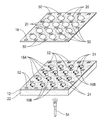
- FIG. 1 is a pictorial representation illustrating the positioning of a flexible substrate over a physically exposed surface of a vacuum chuck.
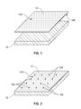
- FIG. 2 is a pictorial representation of the exemplary structure of FIG. 1 after bringing the flexible substrate in direct contact with the physically exposed surface of the vacuum chunk and forming a first set of first electronic components on portions of a physically exposed surface of the flexible substrate, wherein each first electronic component of the first set is orientated in a first direction.
- FIG. 3 is a pictorial representation of the exemplary structure of FIG. 2 after forming a second set of second electronic components on other portions of the physically exposed surface of the flexible substrate, and each second electronic component of the second set is orientated in a second direction which is different from the first direction.
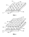
- FIG. 4 is a pictorial representation of the exemplary structure of FIG. 3 after positioning a frame over the physically exposed surface of the flexible substrate, wherein the frame contains a plurality of openings, which each opening is configured to expose a neighboring pair of a first electronic component of the first set and a second electronic component of the second set.
- FIG. 5 is a pictorial representation of the exemplary structure of FIG. 4 after bringing the frame in direct contact with the physically exposed surface of the flexible substrate, and removing the resultant structure from the vacuum chuck.
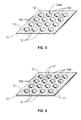
- FIG. 6 is a pictorial representation of the exemplary structure of FIG. 5 after performing a first laser cut to provide openings in the flexible substrate, each opening is surrounded by a remaining portion of the flexible substrate.
- FIG. 7 is a pictorial representation of an optical component holder containing optical components that can be employed in the present application.
- FIG. 8 is a pictorial representation of the exemplary structure of FIG. 7 after positioning the exemplary structure of FIG. 5 over the optical component holder.
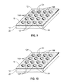
- FIG. 9 is a pictorial representation of the exemplary structure of FIG. 8 after placing the structures in contact with each other.
- FIG. 10 is a pictorial representation of the exemplary structure of FIG. 9 after performing a second laser cut to provide individual pre-electro-optical module assemblies in accordance with one embodiment of the present application.
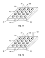
- FIG. 11 is a pictorial representation of the exemplary structure of FIG. 10 after removing the frame.
- FIG. 12 is a pictorial representation of the exemplary structure of FIG. 11 during adhesive dispensing.
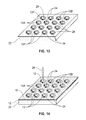
- FIG. 13 is a pictorial representation of the exemplary structure of FIG. 12 after affixing a micro-energy source to the adhesive applied to each pre-electro-optical module assembly.
- FIG. 14 is a pictorial representation of the exemplary structure of FIG. 9 during adhesive dispensing in accordance with another embodiment of the present application.
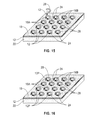
- FIG. 15 is a pictorial representation of the exemplary structure of FIG. 14 after affixing a micro-energy source to the adhesive.
- FIG. 16 is a pictorial representation of the exemplary structure shown in FIG. 15 after performing a second laser cut to provide individual electro-optical module assemblies in accordance with one embodiment of the present application.
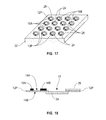
- FIG. 17 is a pictorial representation of the exemplary structure shown in FIG. 16 after removing the frame.
- FIG. 18 is a pictorial representation of one of the electro-optical module assemblies of the present application.
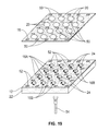
- FIG. 19 is a pictorial representation of a frame containing openings and integrated probes located on one surface thereof, and a corresponding flexible substrate that contains a plurality of areas for electro-optical module assembly and integrated traces and pads for electrical testing that can be employed in accordance with yet another embodiment of the present application.
- FIG. 1 there is represented an initial stage of the method of present application in which a flexible substrate 12 is positioned over a physically exposed surface of a vacuum chuck 10 .
- the positioning may be performed by hand or by utilizing a mechanical device such as, for example, a robot arm.
- the flexible substrate 12 may, or may not, have the same dimension and/or shape as the physically exposed surface of the vacuum chuck 10 .
- the vacuum chuck 10 that is employed in the present application can be rotated in a clock-wise direction, a counter clock-wise direction or both a clock-wise direction and a counter clock-wise direction.
- the vacuum chuck 10 includes a surface that contains a plurality of through holes located therein in which a vacuum can be subsequently applied thereto to hold a work-piece onto the surface of the vacuum chuck 10 .
- the work-piece is a flexible substrate 12 .
- the flexible substrate 12 that can be used in the present application may be composed of a flexible plastic material such as, for example, a polyimide, a polyether ketone (PEEK) or a transparent conductive polyester.
- the flexible substrate 12 that can be employed in the present application can conform to any desired shape or it can flex during its use.
- the flexible substrate 12 that is employed in the present application is not flat or planar; however upon subsequent placement onto the vacuum chuck 10 , the flexible substrate 10 is flat.
- the flexible substrate 12 has a first surface 14 A and a second surface 14 B that is opposite the first surface 14 B.
- the second surface 14 B of the flexible substrate 12 is to be placed on, and held directly to, the surface of the vacuum chuck 10 that contains the plurality of through holes.
- the first surface 14 A of the flexible substrate 12 that is opposite the second surface 14 B of the flexible substrate 12 will be physically exposed and can be subjected to further processing.
- FIG. 2 there is illustrated the exemplary structure of FIG. 1 after bringing the flexible substrate 12 in direct contact with the physically exposed surface of the vacuum chunk 10 and forming a first set of first electronic components 16 A on portions of a physically exposed surface, i.e., the first surface 14 A, of the flexible substrate 12 .
- each first electronic component 16 A of the first set is orientated in a first direction.
- the term “electronic component” is used throughout the present application to denote any device that can transmit and/or receive an electronic signal.
- the flexible substrate 12 is brought in direct contact with the physically exposed surface of the vacuum chunk 10 by applying a vacuum to the through holes located in the surface of the vacuum chuck 10 that is of sufficient force/strength to bring the positioned flexible substrate 12 in direct physical contact with the vacuum chuck 10 .
- the vacuum chuck 10 may be rotated after direct physical contact between the flexible substrate 12 and the vacuum chuck 10 is made. The vacuum is maintained during the forming of the first set of first electronic components 16 A.
- Each first electronic component 16 A can be formed onto the first surface 14 A of the flexible substrate 12 by first selecting an area on the first surface 14 A of the flexible substrate 12 for forming each first electronic component 16 A and thereafter attaching each first electronic component 16 A to the selected areas of the flexible substrate 12 ; the selecting and attaching may be referred to as a pick and place method.
- the attaching may be performed utilizing a solder bump that can be formed on a physically exposed surface of each first electronic component 16 A and/or selected portions of the first surface of the flexible substrate 12 .
- a solder reflow is performed to form a permanent solder joint between the first surface 14 A of the flexible substrate 12 and each first electronic component 16 A.
- each first electronic component 16 A of the first set includes a semiconductor die.
- a semiconductor die i.e., semiconductor chip
- the semiconductor die that may be used as each first electronic component 16 A may be formed utilizing techniques that are well known to those skilled in the art.
- each first set of first electronic components 16 A includes a RF attenna.
- a RF antenna includes a metal trace coil.
- the RF attenna that may be used as each first electronic component 16 A may be formed utilizing techniques that are well known to those skilled in the art.
- FIG. 3 there is illustrated the exemplary structure of FIG. 2 after forming a second set of second electronic components 16 B on other portions of the physically exposed surface (i.e., the first surface 14 A) of the flexible substrate 12 , wherein each second electronic component 14 B of the second set is orientated in a second direction which is different from the first direction.
- this step of the present application may be omitted.
- the forming of the second electronic components 16 B can be performed by first rotating the vacuum chuck 10 .
- the rotation may be in a clock-wise direction or a counter clock-wise direction.
- the rotation is performed while maintaining the vacuum so as to hold the flexible substrate 10 on the vacuum chuck 10 .
- the second set of second electronic components 16 B are attached to selected areas of the flexible substrate 12 ; i.e., a second pick and place method is used.
- the attaching may be performed utilizing a solder bump that can be formed on a physically exposed surface of each second electronic component 16 B and/or selected portions of the first surface of the flexible substrate 12 .
- a solder reflow is performed to form a permanent solder joint between the first surface 14 A of the flexible substrate 12 and each second electronic component 16 B.
- Each second electronic component 16 B may include one of the electronic components mentioned above for the first set of first electronic components 16 A.
- each second electronic component 16 B includes a same electronic component as each first electronic component 16 A.
- each first electronic component 16 A may be a first semiconductor die, while each second electronic component 16 B may be a second semiconductor die.
- each second electronic component 16 B includes a different electronic component than each first electronic component 16 A.
- each first electronic component 16 A may be a semiconductor die, while each second electronic component 16 B may be an RF antenna.
- first and second electronic components 16 A, 16 B
- the first and second electronic components 16 A, 16 B are configured such that each first electronic component 16 A is associated with, and in proximity to, one of the second electronic components 16 B.
- FIG. 4 there is illustrated the exemplary structure of FIG. 3 after positioning a frame 18 over the physically exposed surface (i.e., first surface 14 A) of the flexible substrate 12 , wherein the frame 18 contains a plurality of openings 20 .
- Each opening 20 is configured to expose a neighboring pair of a first electronic component 16 A of the first set and a second electronic component 16 B of the second set.
- the positioning may be performed by hand or by utilizing a mechanical device such as, for example, a robot arm.
- the frame 18 may, or may not, have the same dimension and/or shape as the flexible substrate 12 .
- the frame 18 may be composed of various materials including, for example, a metal.
- the openings 20 that are present in the frame 18 may be formed utilizing techniques well known to those skilled in the art including, but not limited to, lithography and etching, laser cutting, and sawing.
- Each opening 20 within the frame 18 has a same shape. In one embodiment, and as shown in FIG. 4 , each opening 20 of the frame 18 is circular. Other shapes such as, for example, rectangular, are contemplated and can be used as the shape of each opening 20 of frame 18 .
- Each opening 20 of the frame 18 is configured to define an electro-optical module assembly area of the flexible substrate 12 .
- an electro-optical module assembly area it is meant an area of the flexible substrate 12 in which an electro-optical module assembly will be subsequently formed.
- each opening 20 may have a diameter of from 1 mm to 15 mm. The diameter/perimeter of each opening 20 will be used to define the outer diameter/perimeter of each electro-optical module assembly to be subsequently formed.
- the frame 18 may contain various securing elements/components for attaching frame 18 to the physically exposed surface (i.e., the first surface 14 A) of the flexible substrate 12 .
- the frame 18 may contain hinge elements or tape segments.
- FIG. 5 there is illustrated the exemplary structure of FIG. 4 after bringing the frame 18 in direct contact with the physically exposed surface (i.e., first surface 14 A) of the flexible substrate 12 , and removing the resultant structure from the vacuum chuck 10 .
- the bringing of the two structures together can be performed by hand or by utilizing a mechanical device such as, for example, a robot arm.
- the frame 18 can be secured to the physically exposed surface (i.e., first surface 14 A) of the flexible substrate 12 utilizing the securing elements/components present on the frame 18 .
- the vacuum may be stopped and thereafter the framed structure ( 12 / 18 ) is then removed from the vacuum chuck.
- each opening 20 exposes an electro-optical module assembly area (denoted as “Area” in FIG. 5 ) of the flexible substrate 12 .
- each opening 17 is located in an inner portion of one of the electro-optical module assembly areas and is surrounded by a remaining portion of the flexible substrate 12 .
- Each opening 17 may have any shape and size provided that it remains in one of the electro-optical module assembly areas of the flexible substrate 12 and that a portion of the flexible substrate 12 surrounds the opening 17 .
- each opening 17 is circular and is used to provide an inner diameter of the electro-optical module assembly to be subsequently formed.
- the inner diameter of the electro-optical module assembly to be subsequently formed that is provided by each opening 17 is from 1 mm to 15 mm.
- Each opening 17 provides a window for a subsequently formed optical component.
- Laser cutting may be performed utilizing any laser cutting apparatus that is well known to those skilled in the art.
- the optical component holder 22 may be composed of any material such as, for example, a plastic or a metal.
- the optical component holder 22 may be configured to contain openings partially formed therein for holding each optical component 24 .
- the optical component holder 22 may be configured to include a plurality of vacuum holes for holding edges of each optical component 24 to a surface of the optical component holder 22 .
- the optical component holder 22 may contain various securing elements/components for attaching the optical component holder 22 to second surface 14 B of the framed structure frame ( 12 / 18 ).
- the optical component holder 22 may contain hinge elements or tape segments.
- optical component is used throughout the present application to denote an element that changes the behavior of, bend, or conduct light.
- Optical components 24 that can be employed in the present application include, for example, a mirror; a lens including a camera lens, or a contact lens, a prism, an optical filter, or a light emitting diode.
- the optical components 24 can be formed utilizing techniques well known in the art. In some embodiments, the optical components 24 may be formed in the optical component holder 22 itself. After providing the optical components 24 to the optical component holder 22 , an adhesive (conductive or non-conductive) may be applied around the perimeter, i.e., rim, of a physically exposed surface of each optical component 24 .
- an adhesive conductive or non-conductive
- FIG. 8 there is illustrated the exemplary structure of FIG. 7 after positioning the exemplary structure of FIG. 5 (i.e., the framed structure 12 / 18 ) over the optical component holder 22 .
- the positioning may be performed by hand or by utilizing a mechanical device such as, for example, a robot arm.
- the optical component holder 22 may, or may not, have the same dimension and/or shape as the framed structure ( 12 / 18 ) of FIG. 5 .
- the positioning is such that each optical component 24 of the optical holder component 22 will be subsequently positioned within one of the electro-optical module assembly areas and that a portion of each optical component 24 can be visible through opening 17 that was previously formed in each electro-optical module assembly area.
- the positioning is such that the second surface 14 B of the flexible substrate 12 will face the surface of the optical component holder 22 containing the optical components 24 .
- FIG. 9 there is illustrated the exemplary structure of FIG. 8 after bringing the structures shown in FIG. 6 in contact with each other.
- the bringing of the two structures in contact with each other can be performed by hand or by utilizing a mechanical placing device such as, for example, a robot arm.
- the second surface 14 B of the flexible substrate 12 is now in direct physical contact with the surface of the optical component holder 22 containing the optical components 24 .
- a cure step may now be performed to transfer each of the optical components 24 to one of the electro-optical module assembly areas.
- the curing step provides a permanent bond between the adhesive applied to each optical component 24 to the second surface 14 B of the flexible substrate 12 .
- the vacuum may or may not be maintained during the curing step.
- pre-electro-optical module assemblies denotes incomplete, i.e., unfinished, electro-optical module assemblies which lack one or more components.
- each resultant pre-electro-optical module assemblies lacks a micro-energy source, but includes a remaining portion of the flexible substrate 12 P, an electronic component (i.e., first and second electronic components 16 A, 16 B) and an optical component 24 .
- each remaining portion of the flexible substrate 12 P is ring-shaped.
- the ring-shaped has an outer wall having an outer diameter and an inner wall having an inner diameter, wherein the inner diameter is less than the outer diameter, and the inner diameter is defined by a dimension of the opening 17 and the outer diameter is defined the dimension of the opening 20 formed in the frame 18 .
- Laser cutting may be performed utilizing any laser cutting apparatus that is well known to those skilled in the art.
- the laser cutting is performed around the edges of each opening 20 formed in the frame 18 .
- This step of the present application provides the outer diameter/perimeter of each electro-optical module assembly to be subsequently formed. In one embodiment, this laser cutting step results in a circular pre-electro-optical module assembly.
- FIG. 11 there is illustrated the exemplary structure of FIG. 10 after removing the frame 18 and remaining portions of the flexible substrate 12 that are not used in providing each pre-electro-optical module assembly.
- the frame 18 and the remaining portions of the flexible substrate 12 that are not used in providing each pre-electro-optical module assembly may be removed by hand or by mechanical means such as a robot arm.
- Each pre-electro-optical module assembly ( 12 P/ 16 A/ 16 B/ 24 ) remains on a surface of the optical component holder 22 .
- a vacuum may or may not be maintained to the optical component holder 22 throughout the removal of the frame 18 and the remaining portions of the flexible substrate 12 that are not used in providing each pre-electro-optical module assembly.
- the adhesive which may be conductive or non-conductive, is applied to a portion of the first surface of each remaining portion of the flexible substrate 12 P that is used in providing each pre-electro-optical module assembly utilizing techniques well known to those skilled in the art.
- a vacuum may or may not be maintained to the optical component holder 22 throughout this step of present application.
- FIG. 13 there is illustrated the exemplary structure of FIG. 12 after affixing a micro-energy source 28 to the adhesive applied to each pre-electro-optical module assembly; although a single micro-energy source is described and illustrated, a plurality can be formed in each electro-optical module assembly area.
- the affixing includes picking a micro-energy source 28 , placing the micro-energy source 28 on the adhesive applied to the each pre-electro-optical module assembly provided in FIG. 12 , and curing to form a permanent bond.
- micro-energy source it is meant any energy source whose dimension is less than 1,000 microns.
- micro-energy source 28 examples include, but are not limited to, capacitors and micro-batteries. Each micro-energy source 28 can be formed utilizing techniques well known to those skilled in the art. A vacuum may or may not be maintained to the optical component holder 22 throughout this step of present application. After affixing, the vacuum applied to the optical component holder 22 may be turned off, and each electro-optical module assembly can be removed from the surface of the optical component holder 22 .
- Each electro-optical module assembly (see, FIG. 19 ) includes a flexible substrate 12 P having a first surface 14 A and a second surface 14 B opposite the first surface 14 A.
- the flexible substrate 12 P contains an opening 17 located therein that extends from the first surface 14 A to the second surface 14 B.
- the electro-optical module assembly further includes an optical component 24 located on the second surface 14 B of the flexible substrate 12 P and positioned to have a surface exposed by the opening 17 , at least one electronic component ( 16 A, 16 B) located on a first portion of the first surface 14 A of the flexible substrate 12 P, and at least one micro-energy source 28 located on a second portion of the first surface 14 B of the flexible substrate 12 P.
- FIG. 14 there is illustrated the exemplary structure of FIG. 9 during adhesive dispensing 26 in accordance with another embodiment of the present application.
- the adhesive dispensing 26 is performed prior to performing the second laser cutting process.
- the adhesive which may be conductive or non-conductive, is applied to a portion of the first surface of each flexible substrate 12 that present in each electro-optical module assembly area utilizing techniques well known to those skilled in the art.
- a vacuum may or may not be maintained to the optical component holder 22 throughout this step of present application.
- FIG. 15 there is a pictorial representation of the exemplary structure of FIG. 14 after affixing a micro-energy source 28 (as defined above) to the adhesive; although a single micro-energy source is described and illustrated, a plurality can be formed in each electro-optical module assembly area.
- the affixing includes picking a micro-energy source 28 , placing the micro-energy source 28 on the adhesive applied to the each electro-optical module assembly area, and curing to form a permanent bond.
- a vacuum may or may not be maintained to the optical component holder 22 throughout this step of present application.
- FIG. 16 there is illustrated the exemplary structure shown in FIG. 15 after performing a second laser cut to provide individual electro-optical module assemblies in accordance with one embodiment of the present application.
- Laser cutting may be performed utilizing any laser cutting apparatus that is well known to those skilled in the art.
- the laser cutting is performed around the edges of each opening 20 formed in the frame 18 .
- This step of the present application provides the outer diameter/perimeter of each electro-optical module assembly.
- this laser cutting step results in a circular electro-optical module assembly.
- each remaining portion of the flexible substrate 12 P that is provided by the second laser cutting process is ring-shaped.
- the ring-shaped has an outer wall having an outer diameter and an inner wall having an inner diameter, wherein the inner diameter is less than the outer diameter, and the inner diameter is defined by a dimension of the opening 17 and the outer diameter is defined the dimension of the opening 20 formed in the frame 18 .
- Each electro-optical module assembly (see, FIG. 18 ) includes a flexible substrate 12 P having a first surface 14 A and a second surface 14 B opposite the first surface 14 A.
- the flexible substrate 12 P contains an opening 17 located therein that extends from the first surface 14 A to the second surface 14 B.
- the electro-optical module assembly further includes an optical component 24 located on the second surface 14 B of the flexible substrate 12 P and positioned to have a surface exposed by the opening 17 , at least one electronic component ( 16 A, 16 B) located on a first portion of the first surface 14 A of the flexible substrate 12 P, and at least one micro-energy source 28 located on a second portion of the first surface 14 B of the flexible substrate 12 P.
- FIG. 17 there is illustrated the exemplary structure shown in FIG. 16 after removing the frame 18 and remaining portions of the flexible substrate 12 that are not used in providing each electro-optical module assembly.
- the frame 18 and the remaining portions of the flexible substrate 12 that are not used in providing each electro-optical module assembly may be removed by hand or by mechanical means such as a robot arm.
- Each electro-optical module assembly ( 12 P/ 16 A/ 16 B/ 24 / 28 ) remains on a surface of the optical component holder 22 .
- a vacuum may or may not be maintained to the optical component holder 22 throughout the removal of the frame 18 and the remaining portions of the flexible substrate 12 that are not used in providing each electro-optical module assembly.
- the vacuum may be turned off after the second laser cutting step.
- the electro-optical module assembly includes a flexible substrate 12 P having a first surface 14 A and a second surface 14 B opposite the first surface 14 A.
- the flexible substrate 12 P contains an opening 17 located therein that extends from the first surface 14 A to the second surface 14 B.
- the electro-optical module assembly further includes an optical component 24 located on the second surface 14 B of the flexible substrate 12 P and positioned to have a surface exposed by the opening 17 , at least one electronic component ( 16 A, 16 B) located on a first portion of the first surface 14 A of the flexible substrate 12 P, and at least one micro-energy source 28 located on a second portion of the first surface 14 B of the flexible substrate 12 P.
- the optical component 24 , the at least one electronic component ( 16 A, 16 B) and the at least one micro-energy source 28 are in electrical communication with each other.
- FIG. 19 there is illustrated a test structure containing a frame 18 containing openings 22 and integrated probes 50 located on one surface thereof, and a corresponding flexible substrate 12 that contains first and second electronic components ( 16 A, 16 B), optical components 24 and integrated traces and pads 52 for electrical testing that can be employed in accordance with yet another embodiment of the present application.
- the frame 18 , flexible substrate 12 , first and second electronic components ( 16 A, 16 B), and optical components 24 used in this embodiment of the present application are the same as in previous embodiments of the present application.
- the integrated probes 50 include a conductive metal can be formed utilizing techniques well known those skilled in the art.
- the integrated traces and pads 52 are composed of conductive metals and can be formed utilizing techniques well known in the art.
- the integrated probes 50 of the frame 18 and the integrated traces and pads 52 of the flexible substrate 12 are configured to contact each other upon contacting the frame 18 with the flexible substrate 12 .
- each opening 20 in the frame 18 is configured to expose one of the areas for forming one of the electro-optical module assemblies.
- the test structure even further includes a light source 54 located beneath the flexible substrate 12 .
- An optical component holder 22 as defined above can be located between the flexible substrate 12 and the light source 54 .
- the text structure shown in FIG. 20 can be used to test each individual electro-optical module assembly that is formed.
Landscapes
- Engineering & Computer Science (AREA)
- Microelectronics & Electronic Packaging (AREA)
- Manufacturing & Machinery (AREA)
- Physics & Mathematics (AREA)
- General Physics & Mathematics (AREA)
- Optics & Photonics (AREA)
- Micromachines (AREA)
Abstract
Description
- The present application relates to structures containing electronic components, energy sources and optical components integrated on a flexible substrate. More particularly, the present application relates to an integrated electronic optical (i.e. electro-optical) module assembly, and a method for forming the same.
- Electro-optical module integration is critical for many applications such as, for example, miniaturized cameras (i.e., cell phone cameras), digital microscopes, electronic eyeglasses, and electronic contact lens. These electro-optical modules usually require assembly of various complex components such as, for example, semiconductor die, photodiode/LED, micro-energy source, and optical lens. Electronic components, micro-energy sources, and optical lens usually have different form factors and processing requirements. Therefore, it is difficult to implement a batch process for high volume production of the electro-optical modules. There is thus a need for providing a method that can efficiently fabricate integrated electro-optical module assemblies in a high volume.
- In one aspect of the present application, an electro-optical module assembly is provided. In one embodiment, the electro-optical module assembly includes a flexible substrate having a first surface and a second surface opposite the first surface, wherein the flexible substrate contains an opening located therein that extends from the first surface to the second surface. An optical component is located on the second surface of the flexible substrate and is positioned to have a surface exposed by the opening. At least one electronic component is located on a first portion of the first surface of the flexible substrate, and at least one micro-energy source is located on a second portion of the first surface of the flexible substrate.
- In another aspect of the present application, a test structure for use in electro-optical module assembly is provided. In one embodiment, the test structure includes a frame containing a plurality of openings and having a plurality of integrated probes located on a surface thereof. The test structure further includes a flexible substrate comprising areas for forming electro-optical module assemblies, the flexible substrate containing integrated traces and pads for electrical testing located on a surface thereof. The integrated probes of the frame and the integrated traces and pads of the flexible substrate are configured to contact each other upon contacting the frame with the flexible substrate. In accordance with the present application, each opening in the frame is configured to expose one of the areas for forming one of the electro-optical module assemblies. The test structure even further includes a light source located beneath the flexible substrate.
- In a further aspect of the present application, methods of forming a plurality of electro-optical module assemblies are provided. In one embodiment, the method includes providing a flexible substrate containing a first surface and a second surface opposite the first surface, the first surface including a plurality of electronic components located thereon. Next, a frame containing openings therein is brought into contact with the first surface of the flexible substrate, wherein each opening of the frame physically exposes at least one of the electric components and an electro-optical module assembly area of the flexible substrate. An opening is then formed in an inner portion of each electro-optical module assembly area of the flexible substrate utilizing the frame as a mask. Next, an optical component is affixed to the second surface of the flexible substrate and within each electro-optical module assembly area of the flexible substrate, wherein each opening in the electro-optical module assembly area of the flexible substrate exposes a portion of one of the optical components. Outermost portions of each electro-optical module assembly area of the flexible substrate exposed by each opening in the frame are then cut to provide a plurality of pre-electro-optical module assemblies having the first and second surfaces. Next, at least one micro-energy source is provided to the first surface of each pre-electro-optical module assembly.
- In another embodiment, the method includes providing a flexible substrate containing a first surface and a second surface opposite the first surface, the first surface including a plurality of electronic components located thereon. Next, a frame containing openings therein is brought into contact with the first surface of the flexible substrate, wherein each opening of the frame physically exposes at least one of the electric components and an electro-optical module assembly area of the flexible substrate. An opening is then formed in the inner portion of each electro-optical module assembly area of the flexible substrate utilizing the frame as a mask. Next, an optical component is affixed to the second surface of the flexible substrate and within each electro-optical module assembly area of the flexible substrate, wherein each opening in the electro-optical module assembly area of the flexible substrate exposes a portion of one of the optical components. At least one micro-energy source is then formed within the electro-optical module assembly area and on the first surface of the flexible substrate, and thereafter outermost exposed portions of each electro-optical module assembly area of the flexible substrate exposed by each opening in the frame are cut to provide the electro-optical module assemblies.
-
FIG. 1 is a pictorial representation illustrating the positioning of a flexible substrate over a physically exposed surface of a vacuum chuck. -
FIG. 2 is a pictorial representation of the exemplary structure ofFIG. 1 after bringing the flexible substrate in direct contact with the physically exposed surface of the vacuum chunk and forming a first set of first electronic components on portions of a physically exposed surface of the flexible substrate, wherein each first electronic component of the first set is orientated in a first direction. -
FIG. 3 is a pictorial representation of the exemplary structure ofFIG. 2 after forming a second set of second electronic components on other portions of the physically exposed surface of the flexible substrate, and each second electronic component of the second set is orientated in a second direction which is different from the first direction. -
FIG. 4 is a pictorial representation of the exemplary structure ofFIG. 3 after positioning a frame over the physically exposed surface of the flexible substrate, wherein the frame contains a plurality of openings, which each opening is configured to expose a neighboring pair of a first electronic component of the first set and a second electronic component of the second set. -
FIG. 5 is a pictorial representation of the exemplary structure ofFIG. 4 after bringing the frame in direct contact with the physically exposed surface of the flexible substrate, and removing the resultant structure from the vacuum chuck. -
FIG. 6 is a pictorial representation of the exemplary structure ofFIG. 5 after performing a first laser cut to provide openings in the flexible substrate, each opening is surrounded by a remaining portion of the flexible substrate. -
FIG. 7 is a pictorial representation of an optical component holder containing optical components that can be employed in the present application. -
FIG. 8 is a pictorial representation of the exemplary structure ofFIG. 7 after positioning the exemplary structure ofFIG. 5 over the optical component holder. -
FIG. 9 is a pictorial representation of the exemplary structure ofFIG. 8 after placing the structures in contact with each other. -
FIG. 10 is a pictorial representation of the exemplary structure ofFIG. 9 after performing a second laser cut to provide individual pre-electro-optical module assemblies in accordance with one embodiment of the present application. -
FIG. 11 is a pictorial representation of the exemplary structure ofFIG. 10 after removing the frame. -
FIG. 12 is a pictorial representation of the exemplary structure ofFIG. 11 during adhesive dispensing. -
FIG. 13 is a pictorial representation of the exemplary structure ofFIG. 12 after affixing a micro-energy source to the adhesive applied to each pre-electro-optical module assembly. -
FIG. 14 is a pictorial representation of the exemplary structure ofFIG. 9 during adhesive dispensing in accordance with another embodiment of the present application. -
FIG. 15 is a pictorial representation of the exemplary structure ofFIG. 14 after affixing a micro-energy source to the adhesive. -
FIG. 16 is a pictorial representation of the exemplary structure shown inFIG. 15 after performing a second laser cut to provide individual electro-optical module assemblies in accordance with one embodiment of the present application. -
FIG. 17 is a pictorial representation of the exemplary structure shown inFIG. 16 after removing the frame. -
FIG. 18 is a pictorial representation of one of the electro-optical module assemblies of the present application. -
FIG. 19 is a pictorial representation of a frame containing openings and integrated probes located on one surface thereof, and a corresponding flexible substrate that contains a plurality of areas for electro-optical module assembly and integrated traces and pads for electrical testing that can be employed in accordance with yet another embodiment of the present application. - The present application will now be described in greater detail by referring to the following discussion and drawings that accompany the present application. It is noted that the drawings of the present application are provided for illustrative purposes only and, as such, the drawings are not drawn to scale. It is also noted that like and corresponding elements are referred to by like reference numerals.
- In the following description, numerous specific details are set forth, such as particular structures, components, materials, dimensions, processing steps and techniques, in order to provide an understanding of the various embodiments of the present application. However, it will be appreciated by one of ordinary skill in the art that the various embodiments of the present application may be practiced without these specific details. In other instances, well-known structures or processing steps have not been described in detail in order to avoid obscuring the present application.
- It will be understood that when an element as a layer, region or substrate is referred to as being “on” or “over” another element, it can be directly on the other element or intervening elements may also be present. In contrast, when an element is referred to as being “directly on” or “directly over” another element, there are no intervening elements present. It will also be understood that when an element is referred to as being “beneath” or “under” another element, it can be directly beneath or under the other element, or intervening elements may be present. In contrast, when an element is referred to as being “directly beneath” or “directly under” another element, there are no intervening elements present.
- Referring first to
FIG. 1 , there is represented an initial stage of the method of present application in which aflexible substrate 12 is positioned over a physically exposed surface of avacuum chuck 10. The positioning may be performed by hand or by utilizing a mechanical device such as, for example, a robot arm. Theflexible substrate 12 may, or may not, have the same dimension and/or shape as the physically exposed surface of thevacuum chuck 10. - The
vacuum chuck 10 that is employed in the present application can be rotated in a clock-wise direction, a counter clock-wise direction or both a clock-wise direction and a counter clock-wise direction. Thevacuum chuck 10 includes a surface that contains a plurality of through holes located therein in which a vacuum can be subsequently applied thereto to hold a work-piece onto the surface of thevacuum chuck 10. In the present application, the work-piece is aflexible substrate 12. Theflexible substrate 12 that can be used in the present application may be composed of a flexible plastic material such as, for example, a polyimide, a polyether ketone (PEEK) or a transparent conductive polyester. Theflexible substrate 12 that can be employed in the present application can conform to any desired shape or it can flex during its use. Thus, theflexible substrate 12 that is employed in the present application is not flat or planar; however upon subsequent placement onto thevacuum chuck 10, theflexible substrate 10 is flat. Theflexible substrate 12 has afirst surface 14A and asecond surface 14B that is opposite thefirst surface 14B. In the illustrated embodiment of the present application, thesecond surface 14B of theflexible substrate 12 is to be placed on, and held directly to, the surface of thevacuum chuck 10 that contains the plurality of through holes. Thefirst surface 14A of theflexible substrate 12 that is opposite thesecond surface 14B of theflexible substrate 12 will be physically exposed and can be subjected to further processing. - Referring now to
FIG. 2 , there is illustrated the exemplary structure ofFIG. 1 after bringing theflexible substrate 12 in direct contact with the physically exposed surface of thevacuum chunk 10 and forming a first set of firstelectronic components 16A on portions of a physically exposed surface, i.e., thefirst surface 14A, of theflexible substrate 12. As is shown, each firstelectronic component 16A of the first set is orientated in a first direction. The term “electronic component” is used throughout the present application to denote any device that can transmit and/or receive an electronic signal. - The
flexible substrate 12 is brought in direct contact with the physically exposed surface of thevacuum chunk 10 by applying a vacuum to the through holes located in the surface of thevacuum chuck 10 that is of sufficient force/strength to bring the positionedflexible substrate 12 in direct physical contact with thevacuum chuck 10. Thevacuum chuck 10 may be rotated after direct physical contact between theflexible substrate 12 and thevacuum chuck 10 is made. The vacuum is maintained during the forming of the first set of firstelectronic components 16A. Each firstelectronic component 16A can be formed onto thefirst surface 14A of theflexible substrate 12 by first selecting an area on thefirst surface 14A of theflexible substrate 12 for forming each firstelectronic component 16A and thereafter attaching each firstelectronic component 16A to the selected areas of theflexible substrate 12; the selecting and attaching may be referred to as a pick and place method. In one embodiment, the attaching may be performed utilizing a solder bump that can be formed on a physically exposed surface of each firstelectronic component 16A and/or selected portions of the first surface of theflexible substrate 12. After attaching, a solder reflow is performed to form a permanent solder joint between thefirst surface 14A of theflexible substrate 12 and each firstelectronic component 16A. - In one embodiment, each first
electronic component 16A of the first set includes a semiconductor die. As known to those skilled in the art, a semiconductor die (i.e., semiconductor chip) includes a semiconductor substrate having one or more semiconductor devices located thereon and/or thereupon, and one or more interconnect levels including wiring structures embedded within an interconnect dielectric material. The semiconductor die that may be used as each firstelectronic component 16A may be formed utilizing techniques that are well known to those skilled in the art. - In another embodiment of the present application, each first set of first
electronic components 16A includes a RF attenna. As known to those skilled in the art, a RF antenna includes a metal trace coil. The RF attenna that may be used as each firstelectronic component 16A may be formed utilizing techniques that are well known to those skilled in the art. - Referring now to
FIG. 3 , there is illustrated the exemplary structure ofFIG. 2 after forming a second set of secondelectronic components 16B on other portions of the physically exposed surface (i.e., thefirst surface 14A) of theflexible substrate 12, wherein each secondelectronic component 14B of the second set is orientated in a second direction which is different from the first direction. In some embodiments, this step of the present application may be omitted. The forming of the secondelectronic components 16B can be performed by first rotating thevacuum chuck 10. The rotation may be in a clock-wise direction or a counter clock-wise direction. The rotation is performed while maintaining the vacuum so as to hold theflexible substrate 10 on thevacuum chuck 10. After rotating the vacuum chuck, the second set of secondelectronic components 16B are attached to selected areas of theflexible substrate 12; i.e., a second pick and place method is used. In one embodiment, the attaching may be performed utilizing a solder bump that can be formed on a physically exposed surface of each secondelectronic component 16B and/or selected portions of the first surface of theflexible substrate 12. After attaching, a solder reflow is performed to form a permanent solder joint between thefirst surface 14A of theflexible substrate 12 and each secondelectronic component 16B. - Each second
electronic component 16B may include one of the electronic components mentioned above for the first set of firstelectronic components 16A. In one embodiment, each secondelectronic component 16B includes a same electronic component as each firstelectronic component 16A. For example, each firstelectronic component 16A may be a first semiconductor die, while each secondelectronic component 16B may be a second semiconductor die. In another embodiment, each secondelectronic component 16B includes a different electronic component than each firstelectronic component 16A. For example, each firstelectronic component 16A may be a semiconductor die, while each secondelectronic component 16B may be an RF antenna. - Notwithstanding the types of first and second electronic components (16A, 16B) employed, the first and second electronic components (16A, 16B) are configured such that each first
electronic component 16A is associated with, and in proximity to, one of the secondelectronic components 16B. - Referring now to
FIG. 4 , there is illustrated the exemplary structure ofFIG. 3 after positioning aframe 18 over the physically exposed surface (i.e.,first surface 14A) of theflexible substrate 12, wherein theframe 18 contains a plurality ofopenings 20. Eachopening 20 is configured to expose a neighboring pair of a firstelectronic component 16A of the first set and a secondelectronic component 16B of the second set. The positioning may be performed by hand or by utilizing a mechanical device such as, for example, a robot arm. Theframe 18 may, or may not, have the same dimension and/or shape as theflexible substrate 12. - The
frame 18 may be composed of various materials including, for example, a metal. Theopenings 20 that are present in theframe 18 may be formed utilizing techniques well known to those skilled in the art including, but not limited to, lithography and etching, laser cutting, and sawing. Eachopening 20 within theframe 18 has a same shape. In one embodiment, and as shown inFIG. 4 , each opening 20 of theframe 18 is circular. Other shapes such as, for example, rectangular, are contemplated and can be used as the shape of each opening 20 offrame 18. - Each
opening 20 of theframe 18 is configured to define an electro-optical module assembly area of theflexible substrate 12. By “an electro-optical module assembly area”, it is meant an area of theflexible substrate 12 in which an electro-optical module assembly will be subsequently formed. In embodiments in which eachopening 20 is circular, each opening 20 may have a diameter of from 1 mm to 15 mm. The diameter/perimeter of eachopening 20 will be used to define the outer diameter/perimeter of each electro-optical module assembly to be subsequently formed. - The
frame 18 may contain various securing elements/components for attachingframe 18 to the physically exposed surface (i.e., thefirst surface 14A) of theflexible substrate 12. For example, theframe 18 may contain hinge elements or tape segments. - Referring now to
FIG. 5 , there is illustrated the exemplary structure ofFIG. 4 after bringing theframe 18 in direct contact with the physically exposed surface (i.e.,first surface 14A) of theflexible substrate 12, and removing the resultant structure from thevacuum chuck 10. The bringing of the two structures together can be performed by hand or by utilizing a mechanical device such as, for example, a robot arm. After contacting the two structures together, theframe 18 can be secured to the physically exposed surface (i.e.,first surface 14A) of theflexible substrate 12 utilizing the securing elements/components present on theframe 18. At this point, the vacuum may be stopped and thereafter the framed structure (12/18) is then removed from the vacuum chuck. The removal may be performed by hand or by utilizing a mechanical device such as, for example, a robot arm. After placing, each opening 20 exposes an electro-optical module assembly area (denoted as “Area” inFIG. 5 ) of theflexible substrate 12. - Referring now to
FIG. 6 , there is illustrated the exemplary structure ofFIG. 5 (i.e., the framedstructure 12/18) after performing a first laser cut to provideopenings 17 in theflexible substrate 12. Eachopening 17 is located in an inner portion of one of the electro-optical module assembly areas and is surrounded by a remaining portion of theflexible substrate 12. Eachopening 17 may have any shape and size provided that it remains in one of the electro-optical module assembly areas of theflexible substrate 12 and that a portion of theflexible substrate 12 surrounds theopening 17. In one embodiment, each opening 17 is circular and is used to provide an inner diameter of the electro-optical module assembly to be subsequently formed. In one embodiment, the inner diameter of the electro-optical module assembly to be subsequently formed that is provided by each opening 17 is from 1 mm to 15 mm. Eachopening 17 provides a window for a subsequently formed optical component. Laser cutting may be performed utilizing any laser cutting apparatus that is well known to those skilled in the art. - Referring now to
FIG. 7 , there is illustrated anoptical component holder 22 containingoptical components 24 that can be employed in the present application. Theoptical component holder 22 may be composed of any material such as, for example, a plastic or a metal. In one embodiment, theoptical component holder 22 may be configured to contain openings partially formed therein for holding eachoptical component 24. In another embodiment, theoptical component holder 22 may be configured to include a plurality of vacuum holes for holding edges of eachoptical component 24 to a surface of theoptical component holder 22. Theoptical component holder 22 may contain various securing elements/components for attaching theoptical component holder 22 tosecond surface 14B of the framed structure frame (12/18). For example, theoptical component holder 22 may contain hinge elements or tape segments. - The term “optical component” is used throughout the present application to denote an element that changes the behavior of, bend, or conduct light.
Optical components 24 that can be employed in the present application include, for example, a mirror; a lens including a camera lens, or a contact lens, a prism, an optical filter, or a light emitting diode. - The
optical components 24 can be formed utilizing techniques well known in the art. In some embodiments, theoptical components 24 may be formed in theoptical component holder 22 itself. After providing theoptical components 24 to theoptical component holder 22, an adhesive (conductive or non-conductive) may be applied around the perimeter, i.e., rim, of a physically exposed surface of eachoptical component 24. - Referring now to
FIG. 8 , there is illustrated the exemplary structure ofFIG. 7 after positioning the exemplary structure ofFIG. 5 (i.e., the framedstructure 12/18) over theoptical component holder 22. The positioning may be performed by hand or by utilizing a mechanical device such as, for example, a robot arm. Theoptical component holder 22 may, or may not, have the same dimension and/or shape as the framed structure (12/18) ofFIG. 5 . The positioning is such that eachoptical component 24 of theoptical holder component 22 will be subsequently positioned within one of the electro-optical module assembly areas and that a portion of eachoptical component 24 can be visible throughopening 17 that was previously formed in each electro-optical module assembly area. Also, the positioning is such that thesecond surface 14B of theflexible substrate 12 will face the surface of theoptical component holder 22 containing theoptical components 24. - Referring now to
FIG. 9 , there is illustrated the exemplary structure ofFIG. 8 after bringing the structures shown inFIG. 6 in contact with each other. The bringing of the two structures in contact with each other can be performed by hand or by utilizing a mechanical placing device such as, for example, a robot arm. At this point of the present application, thesecond surface 14B of theflexible substrate 12 is now in direct physical contact with the surface of theoptical component holder 22 containing theoptical components 24. A cure step may now be performed to transfer each of theoptical components 24 to one of the electro-optical module assembly areas. The curing step provides a permanent bond between the adhesive applied to eachoptical component 24 to thesecond surface 14B of theflexible substrate 12. In embodiments in which theoptical components 24 were held to the surface of theoptical holder component 22 by vacuum, the vacuum may or may not be maintained during the curing step. - Referring now to
FIG. 10 , there is illustrated the exemplary structure ofFIG. 9 after performing a second laser cut to provide individual pre-electro-optical module assemblies in accordance with one embodiment of the present application. The term “pre-electro-optical module assemblies” denotes incomplete, i.e., unfinished, electro-optical module assemblies which lack one or more components. In the illustrated example ofFIG. 10 , each resultant pre-electro-optical module assemblies lacks a micro-energy source, but includes a remaining portion of theflexible substrate 12P, an electronic component (i.e., first and secondelectronic components optical component 24. Theoptical component 24 and the electronic component (16A, 16B) are located on opposite surfaces of the remaining portion of theflexible substrate 12P. In some embodiments, each remaining portion of theflexible substrate 12P is ring-shaped. In such an embodiment, the ring-shaped has an outer wall having an outer diameter and an inner wall having an inner diameter, wherein the inner diameter is less than the outer diameter, and the inner diameter is defined by a dimension of theopening 17 and the outer diameter is defined the dimension of theopening 20 formed in theframe 18. - Laser cutting may be performed utilizing any laser cutting apparatus that is well known to those skilled in the art. The laser cutting is performed around the edges of each opening 20 formed in the
frame 18. This step of the present application provides the outer diameter/perimeter of each electro-optical module assembly to be subsequently formed. In one embodiment, this laser cutting step results in a circular pre-electro-optical module assembly. - Referring now to
FIG. 11 , there is illustrated the exemplary structure ofFIG. 10 after removing theframe 18 and remaining portions of theflexible substrate 12 that are not used in providing each pre-electro-optical module assembly. Theframe 18 and the remaining portions of theflexible substrate 12 that are not used in providing each pre-electro-optical module assembly may be removed by hand or by mechanical means such as a robot arm. Each pre-electro-optical module assembly (12P/16 A/ 16B/24) remains on a surface of theoptical component holder 22. A vacuum may or may not be maintained to theoptical component holder 22 throughout the removal of theframe 18 and the remaining portions of theflexible substrate 12 that are not used in providing each pre-electro-optical module assembly. - Referring now to
FIG. 12 , there is illustrated the exemplary structure ofFIG. 11 during adhesive dispensing 26. The adhesive, which may be conductive or non-conductive, is applied to a portion of the first surface of each remaining portion of theflexible substrate 12P that is used in providing each pre-electro-optical module assembly utilizing techniques well known to those skilled in the art. A vacuum may or may not be maintained to theoptical component holder 22 throughout this step of present application. - Referring now to
FIG. 13 , there is illustrated the exemplary structure ofFIG. 12 after affixing amicro-energy source 28 to the adhesive applied to each pre-electro-optical module assembly; although a single micro-energy source is described and illustrated, a plurality can be formed in each electro-optical module assembly area. The affixing includes picking amicro-energy source 28, placing themicro-energy source 28 on the adhesive applied to the each pre-electro-optical module assembly provided inFIG. 12 , and curing to form a permanent bond. By “micro-energy source” it is meant any energy source whose dimension is less than 1,000 microns. Examples of energy sources that can be employed as themicro-energy source 28 include, but are not limited to, capacitors and micro-batteries. Eachmicro-energy source 28 can be formed utilizing techniques well known to those skilled in the art. A vacuum may or may not be maintained to theoptical component holder 22 throughout this step of present application. After affixing, the vacuum applied to theoptical component holder 22 may be turned off, and each electro-optical module assembly can be removed from the surface of theoptical component holder 22. - Each electro-optical module assembly (see,
FIG. 19 ) includes aflexible substrate 12P having afirst surface 14A and asecond surface 14B opposite thefirst surface 14A. Theflexible substrate 12P contains anopening 17 located therein that extends from thefirst surface 14A to thesecond surface 14B. The electro-optical module assembly further includes anoptical component 24 located on thesecond surface 14B of theflexible substrate 12P and positioned to have a surface exposed by theopening 17, at least one electronic component (16A, 16B) located on a first portion of thefirst surface 14A of theflexible substrate 12P, and at least onemicro-energy source 28 located on a second portion of thefirst surface 14B of theflexible substrate 12P. - Referring now to
FIG. 14 , there is illustrated the exemplary structure ofFIG. 9 during adhesive dispensing 26 in accordance with another embodiment of the present application. In this embodiment, the adhesive dispensing 26 is performed prior to performing the second laser cutting process. The adhesive, which may be conductive or non-conductive, is applied to a portion of the first surface of eachflexible substrate 12 that present in each electro-optical module assembly area utilizing techniques well known to those skilled in the art. A vacuum may or may not be maintained to theoptical component holder 22 throughout this step of present application. - Referring now to
FIG. 15 , there is a pictorial representation of the exemplary structure ofFIG. 14 after affixing a micro-energy source 28 (as defined above) to the adhesive; although a single micro-energy source is described and illustrated, a plurality can be formed in each electro-optical module assembly area. The affixing includes picking amicro-energy source 28, placing themicro-energy source 28 on the adhesive applied to the each electro-optical module assembly area, and curing to form a permanent bond. A vacuum may or may not be maintained to theoptical component holder 22 throughout this step of present application. - Referring now to
FIG. 16 , there is illustrated the exemplary structure shown inFIG. 15 after performing a second laser cut to provide individual electro-optical module assemblies in accordance with one embodiment of the present application. Laser cutting may be performed utilizing any laser cutting apparatus that is well known to those skilled in the art. The laser cutting is performed around the edges of each opening 20 formed in theframe 18. This step of the present application provides the outer diameter/perimeter of each electro-optical module assembly. In one embodiment, this laser cutting step results in a circular electro-optical module assembly. In some embodiments, each remaining portion of theflexible substrate 12P that is provided by the second laser cutting process is ring-shaped. In such an embodiment, the ring-shaped has an outer wall having an outer diameter and an inner wall having an inner diameter, wherein the inner diameter is less than the outer diameter, and the inner diameter is defined by a dimension of theopening 17 and the outer diameter is defined the dimension of theopening 20 formed in theframe 18. - Each electro-optical module assembly (see,
FIG. 18 ) includes aflexible substrate 12P having afirst surface 14A and asecond surface 14B opposite thefirst surface 14A. Theflexible substrate 12P contains anopening 17 located therein that extends from thefirst surface 14A to thesecond surface 14B. The electro-optical module assembly further includes anoptical component 24 located on thesecond surface 14B of theflexible substrate 12P and positioned to have a surface exposed by theopening 17, at least one electronic component (16A, 16B) located on a first portion of thefirst surface 14A of theflexible substrate 12P, and at least onemicro-energy source 28 located on a second portion of thefirst surface 14B of theflexible substrate 12P. - Referring now to
FIG. 17 , there is illustrated the exemplary structure shown inFIG. 16 after removing theframe 18 and remaining portions of theflexible substrate 12 that are not used in providing each electro-optical module assembly. Theframe 18 and the remaining portions of theflexible substrate 12 that are not used in providing each electro-optical module assembly may be removed by hand or by mechanical means such as a robot arm. Each electro-optical module assembly (12P/16 A/ 16B/24/28) remains on a surface of theoptical component holder 22. A vacuum may or may not be maintained to theoptical component holder 22 throughout the removal of theframe 18 and the remaining portions of theflexible substrate 12 that are not used in providing each electro-optical module assembly. The vacuum may be turned off after the second laser cutting step. - Referring now to
FIG. 18 , there is an enlarged cross sectional view of one of the electro-optical module assemblies of the present application as provided utilizing the various methods of the present application. The electro-optical module assembly includes aflexible substrate 12P having afirst surface 14A and asecond surface 14B opposite thefirst surface 14A. Theflexible substrate 12P contains anopening 17 located therein that extends from thefirst surface 14A to thesecond surface 14B. The electro-optical module assembly further includes anoptical component 24 located on thesecond surface 14B of theflexible substrate 12P and positioned to have a surface exposed by theopening 17, at least one electronic component (16A, 16B) located on a first portion of thefirst surface 14A of theflexible substrate 12P, and at least onemicro-energy source 28 located on a second portion of thefirst surface 14B of theflexible substrate 12P. In accordance with the present application, theoptical component 24, the at least one electronic component (16A, 16B) and the at least onemicro-energy source 28 are in electrical communication with each other. - Referring now to
FIG. 19 , there is illustrated a test structure containing aframe 18 containingopenings 22 andintegrated probes 50 located on one surface thereof, and a correspondingflexible substrate 12 that contains first and second electronic components (16A, 16B),optical components 24 and integrated traces andpads 52 for electrical testing that can be employed in accordance with yet another embodiment of the present application. Theframe 18,flexible substrate 12, first and second electronic components (16A, 16B), andoptical components 24 used in this embodiment of the present application are the same as in previous embodiments of the present application. The integrated probes 50 include a conductive metal can be formed utilizing techniques well known those skilled in the art. The integrated traces andpads 52 are composed of conductive metals and can be formed utilizing techniques well known in the art. - The integrated probes 50 of the
frame 18 and the integrated traces andpads 52 of theflexible substrate 12 are configured to contact each other upon contacting theframe 18 with theflexible substrate 12. In accordance with the present application, each opening 20 in theframe 18 is configured to expose one of the areas for forming one of the electro-optical module assemblies. The test structure even further includes alight source 54 located beneath theflexible substrate 12. Anoptical component holder 22 as defined above can be located between theflexible substrate 12 and thelight source 54. The text structure shown inFIG. 20 can be used to test each individual electro-optical module assembly that is formed. - While the present application has been particularly shown and described with respect to preferred embodiments thereof, it will be understood by those skilled in the art that the foregoing and other changes in forms and details may be made without departing from the spirit and scope of the present application. It is therefore intended that the present application not be limited to the exact forms and details described and illustrated, but fall within the scope of the appended claims.
Claims (16)
Priority Applications (1)
| Application Number | Priority Date | Filing Date | Title |
|---|---|---|---|
| US15/821,432 US10638613B2 (en) | 2016-05-09 | 2017-11-22 | Method of forming a plurality of electro-optical module assemblies |
Applications Claiming Priority (3)
| Application Number | Priority Date | Filing Date | Title |
|---|---|---|---|
| US201662333525P | 2016-05-09 | 2016-05-09 | |
| US15/452,933 US10670656B2 (en) | 2016-05-09 | 2017-03-08 | Integrated electro-optical module assembly |
| US15/821,432 US10638613B2 (en) | 2016-05-09 | 2017-11-22 | Method of forming a plurality of electro-optical module assemblies |
Related Parent Applications (2)
| Application Number | Title | Priority Date | Filing Date |
|---|---|---|---|
| US15/452,933 Continuation US10670656B2 (en) | 2016-05-09 | 2017-03-08 | Integrated electro-optical module assembly |
| US15/452,933 Continuation-In-Part US10670656B2 (en) | 2016-05-09 | 2017-03-08 | Integrated electro-optical module assembly |
Publications (2)
| Publication Number | Publication Date |
|---|---|
| US20180098432A1 true US20180098432A1 (en) | 2018-04-05 |
| US10638613B2 US10638613B2 (en) | 2020-04-28 |
Family
ID=61758635
Family Applications (1)
| Application Number | Title | Priority Date | Filing Date |
|---|---|---|---|
| US15/821,432 Active 2037-09-26 US10638613B2 (en) | 2016-05-09 | 2017-11-22 | Method of forming a plurality of electro-optical module assemblies |
Country Status (1)
| Country | Link |
|---|---|
| US (1) | US10638613B2 (en) |
Citations (4)
| Publication number | Priority date | Publication date | Assignee | Title |
|---|---|---|---|---|
| US20040258367A1 (en) * | 2003-03-27 | 2004-12-23 | Martin Weigert | Electrooptical module |
| US7129722B1 (en) * | 2002-10-09 | 2006-10-31 | Cypress Semiconductor Corp. | Methods of improving reliability of an electro-optical module |
| JP2009244337A (en) * | 2008-03-28 | 2009-10-22 | Nippon Telegr & Teleph Corp <Ntt> | Method of manufacturing electro-optical module and electro-optical module |
| US20100025793A1 (en) * | 2008-08-01 | 2010-02-04 | Impac Technology Co., Ltd. | Assembly for image sensing chip and assembling method thereof |
Family Cites Families (11)
| Publication number | Priority date | Publication date | Assignee | Title |
|---|---|---|---|---|
| US6812718B1 (en) | 1999-05-27 | 2004-11-02 | Nanonexus, Inc. | Massively parallel interface for electronic circuits |
| KR100877243B1 (en) | 2001-02-19 | 2009-01-07 | 니혼 덴산 리드 가부시끼가이샤 | Circuit board inspection apparatus and method for inspecting a circuit board |
| JP2006047682A (en) | 2004-08-04 | 2006-02-16 | Fujitsu Ltd | Substrate and optical device interconnection substrate |
| US8097926B2 (en) | 2008-10-07 | 2012-01-17 | Mc10, Inc. | Systems, methods, and devices having stretchable integrated circuitry for sensing and delivering therapy |
| JP2010223690A (en) | 2009-03-23 | 2010-10-07 | Seiko Epson Corp | Flexible substrate, electro-optical device and electronic apparatus |
| US10441185B2 (en) | 2009-12-16 | 2019-10-15 | The Board Of Trustees Of The University Of Illinois | Flexible and stretchable electronic systems for epidermal electronics |
| US8721074B2 (en) | 2011-11-30 | 2014-05-13 | Johnson & Johnson Vision Care, Inc. | Electrical interconnects in an electronic contact lens |
| EP2856506A4 (en) | 2012-05-29 | 2016-02-17 | Essence Solar Solutions Ltd | PHOTOVOLTAIC MODULE ASSEMBLY |
| US9465236B2 (en) | 2013-03-15 | 2016-10-11 | Johnson & Johnson Vision Care, Inc. | Ophthalmic devices incorporating photonic elements |
| US10096802B2 (en) | 2014-04-08 | 2018-10-09 | International Business Machines Corporation | Homogeneous solid metallic anode for thin film microbattery |
| TWI695970B (en) | 2015-09-17 | 2020-06-11 | 日月光半導體製造股份有限公司 | Optical device, electrical device and passive optical component |
-
2017
- 2017-11-22 US US15/821,432 patent/US10638613B2/en active Active
Patent Citations (4)
| Publication number | Priority date | Publication date | Assignee | Title |
|---|---|---|---|---|
| US7129722B1 (en) * | 2002-10-09 | 2006-10-31 | Cypress Semiconductor Corp. | Methods of improving reliability of an electro-optical module |
| US20040258367A1 (en) * | 2003-03-27 | 2004-12-23 | Martin Weigert | Electrooptical module |
| JP2009244337A (en) * | 2008-03-28 | 2009-10-22 | Nippon Telegr & Teleph Corp <Ntt> | Method of manufacturing electro-optical module and electro-optical module |
| US20100025793A1 (en) * | 2008-08-01 | 2010-02-04 | Impac Technology Co., Ltd. | Assembly for image sensing chip and assembling method thereof |
Also Published As
| Publication number | Publication date |
|---|---|
| US10638613B2 (en) | 2020-04-28 |
Similar Documents
| Publication | Publication Date | Title |
|---|---|---|
| US10326039B2 (en) | Proximity detector device with interconnect layers and related methods | |
| KR100433781B1 (en) | Method for manufacturing semiconductor devices | |
| KR20000011527A (en) | Method for manufacturing a flip chip semiconductor device | |
| JPH07509351A (en) | Method and apparatus for separating circuit dice from wafers | |
| JP6301565B1 (en) | Method and apparatus for separating a microchip from a wafer and mounting the microchip on a substrate | |
| KR20000047438A (en) | Method and apparatus for testing semiconductor devices | |
| US6391679B1 (en) | Method of processing a single semiconductor using at least one carrier element | |
| US20160099285A1 (en) | Method for manufacturing solid-state imaging device and method for manufacturing camera module | |
| TWI549174B (en) | Method of manufacturing a semiconductor device | |
| KR20180033292A (en) | Anisotropic conductive film | |
| JP2009533867A (en) | Method of installing a protective cover on an image pickup apparatus and apparatus manufactured by the method | |
| US9013017B2 (en) | Method for making image sensors using wafer-level processing and associated devices | |
| KR101955663B1 (en) | Membrane sheet with bumps for probe card, probe card and method for manufacturing membrane sheet with bumps for probe card | |
| US10687425B2 (en) | Method of forming a plurality of electro-optical module assemblies | |
| US10638613B2 (en) | Method of forming a plurality of electro-optical module assemblies | |
| US10393798B2 (en) | Integrated electro-optical module assembly | |
| US10670656B2 (en) | Integrated electro-optical module assembly | |
| JP2002289628A (en) | Image recognition method, image recognition device, and semiconductor device manufacturing method and manufacturing device | |
| CN102064092B (en) | Carrier separation method for semiconductor process | |
| JPS61203404A (en) | How to attach a filter to a CCD imager | |
| TWI844659B (en) | Method for manufacturing an optical sensor package | |
| JP2002330358A (en) | Positioning method of optical element and lens assembly | |
| KR101161773B1 (en) | Camera module and manufacturing method | |
| US6449837B1 (en) | Method for attaching electronic devices to metallized glass printed circuit | |
| JP2009277061A (en) | Method for manufacturing semiconductor device |
Legal Events
| Date | Code | Title | Description |
|---|---|---|---|
| AS | Assignment |
Owner name: INTERNATIONAL BUSINESS MACHINES CORPORATION, NEW YORK Free format text: ASSIGNMENT OF ASSIGNORS INTEREST;ASSIGNORS:ANDRY, PAUL S.;CHEN, QIANWEN;DANG, BING;AND OTHERS;SIGNING DATES FROM 20170228 TO 20170306;REEL/FRAME:044202/0096 Owner name: INTERNATIONAL BUSINESS MACHINES CORPORATION, NEW Y Free format text: ASSIGNMENT OF ASSIGNORS INTEREST;ASSIGNORS:ANDRY, PAUL S.;CHEN, QIANWEN;DANG, BING;AND OTHERS;SIGNING DATES FROM 20170228 TO 20170306;REEL/FRAME:044202/0096 |
|
| FEPP | Fee payment procedure |
Free format text: ENTITY STATUS SET TO UNDISCOUNTED (ORIGINAL EVENT CODE: BIG.); ENTITY STATUS OF PATENT OWNER: LARGE ENTITY |
|
| STPP | Information on status: patent application and granting procedure in general |
Free format text: DOCKETED NEW CASE - READY FOR EXAMINATION |
|
| STPP | Information on status: patent application and granting procedure in general |
Free format text: NON FINAL ACTION MAILED |
|
| STPP | Information on status: patent application and granting procedure in general |
Free format text: RESPONSE TO NON-FINAL OFFICE ACTION ENTERED AND FORWARDED TO EXAMINER |
|
| STPP | Information on status: patent application and granting procedure in general |
Free format text: NOTICE OF ALLOWANCE MAILED -- APPLICATION RECEIVED IN OFFICE OF PUBLICATIONS |
|
| STPP | Information on status: patent application and granting procedure in general |
Free format text: NOTICE OF ALLOWANCE MAILED -- APPLICATION RECEIVED IN OFFICE OF PUBLICATIONS |
|
| STCF | Information on status: patent grant |
Free format text: PATENTED CASE |
|
| MAFP | Maintenance fee payment |
Free format text: PAYMENT OF MAINTENANCE FEE, 4TH YEAR, LARGE ENTITY (ORIGINAL EVENT CODE: M1551); ENTITY STATUS OF PATENT OWNER: LARGE ENTITY Year of fee payment: 4 |