US20180098430A1 - Electronic component-embedded substrate and electronic component device - Google Patents
Electronic component-embedded substrate and electronic component device Download PDFInfo
- Publication number
- US20180098430A1 US20180098430A1 US15/718,280 US201715718280A US2018098430A1 US 20180098430 A1 US20180098430 A1 US 20180098430A1 US 201715718280 A US201715718280 A US 201715718280A US 2018098430 A1 US2018098430 A1 US 2018098430A1
- Authority
- US
- United States
- Prior art keywords
- cavity
- core substrate
- electronic component
- wall portion
- insulation wall
- Prior art date
- Legal status (The legal status is an assumption and is not a legal conclusion. Google has not performed a legal analysis and makes no representation as to the accuracy of the status listed.)
- Granted
Links
Images


Classifications
-
- H—ELECTRICITY
- H05—ELECTRIC TECHNIQUES NOT OTHERWISE PROVIDED FOR
- H05K—PRINTED CIRCUITS; CASINGS OR CONSTRUCTIONAL DETAILS OF ELECTRIC APPARATUS; MANUFACTURE OF ASSEMBLAGES OF ELECTRICAL COMPONENTS
- H05K1/00—Printed circuits
- H05K1/18—Printed circuits structurally associated with non-printed electric components
- H05K1/182—Printed circuits structurally associated with non-printed electric components associated with components mounted in printed circuit boards [PCB], e.g. insert-mounted components [IMC]
- H05K1/183—Printed circuits structurally associated with non-printed electric components associated with components mounted in printed circuit boards [PCB], e.g. insert-mounted components [IMC] associated with components mounted in and supported by recessed areas of the PCBs
-
- H01L21/4857—
-
- H01L21/486—
-
- H01L23/3185—
-
- H01L23/49822—
-
- H01L23/49827—
-
- H01L23/49838—
-
- H01L24/16—
-
- H—ELECTRICITY
- H05—ELECTRIC TECHNIQUES NOT OTHERWISE PROVIDED FOR
- H05K—PRINTED CIRCUITS; CASINGS OR CONSTRUCTIONAL DETAILS OF ELECTRIC APPARATUS; MANUFACTURE OF ASSEMBLAGES OF ELECTRICAL COMPONENTS
- H05K1/00—Printed circuits
- H05K1/02—Details
- H05K1/11—Printed elements for providing electric connections to or between printed circuits
- H05K1/115—Via connections; Lands around holes or via connections
-
- H—ELECTRICITY
- H05—ELECTRIC TECHNIQUES NOT OTHERWISE PROVIDED FOR
- H05K—PRINTED CIRCUITS; CASINGS OR CONSTRUCTIONAL DETAILS OF ELECTRIC APPARATUS; MANUFACTURE OF ASSEMBLAGES OF ELECTRICAL COMPONENTS
- H05K1/00—Printed circuits
- H05K1/18—Printed circuits structurally associated with non-printed electric components
- H05K1/182—Printed circuits structurally associated with non-printed electric components associated with components mounted in printed circuit boards [PCB], e.g. insert-mounted components [IMC]
- H05K1/185—Printed circuits structurally associated with non-printed electric components associated with components mounted in printed circuit boards [PCB], e.g. insert-mounted components [IMC] associated with components encapsulated in the insulating substrate of the PCBs; associated with components incorporated in internal layers of multilayer circuit boards
-
- H—ELECTRICITY
- H05—ELECTRIC TECHNIQUES NOT OTHERWISE PROVIDED FOR
- H05K—PRINTED CIRCUITS; CASINGS OR CONSTRUCTIONAL DETAILS OF ELECTRIC APPARATUS; MANUFACTURE OF ASSEMBLAGES OF ELECTRICAL COMPONENTS
- H05K3/00—Apparatus or processes for manufacturing printed circuits
- H05K3/0011—Working of insulating substrates or insulating layers
-
- H—ELECTRICITY
- H05—ELECTRIC TECHNIQUES NOT OTHERWISE PROVIDED FOR
- H05K—PRINTED CIRCUITS; CASINGS OR CONSTRUCTIONAL DETAILS OF ELECTRIC APPARATUS; MANUFACTURE OF ASSEMBLAGES OF ELECTRICAL COMPONENTS
- H05K3/00—Apparatus or processes for manufacturing printed circuits
- H05K3/30—Assembling printed circuits with electric components, e.g. with resistors
- H05K3/301—Assembling printed circuits with electric components, e.g. with resistors by means of a mounting structure
-
- H—ELECTRICITY
- H10—SEMICONDUCTOR DEVICES; ELECTRIC SOLID-STATE DEVICES NOT OTHERWISE PROVIDED FOR
- H10W—GENERIC PACKAGES, INTERCONNECTIONS, CONNECTORS OR OTHER CONSTRUCTIONAL DETAILS OF DEVICES COVERED BY CLASS H10
- H10W70/00—Package substrates; Interposers; Redistribution layers [RDL]
- H10W70/01—Manufacture or treatment
- H10W70/05—Manufacture or treatment of insulating or insulated package substrates, or of interposers, or of redistribution layers
-
- H—ELECTRICITY
- H10—SEMICONDUCTOR DEVICES; ELECTRIC SOLID-STATE DEVICES NOT OTHERWISE PROVIDED FOR
- H10W—GENERIC PACKAGES, INTERCONNECTIONS, CONNECTORS OR OTHER CONSTRUCTIONAL DETAILS OF DEVICES COVERED BY CLASS H10
- H10W70/00—Package substrates; Interposers; Redistribution layers [RDL]
- H10W70/60—Insulating or insulated package substrates; Interposers; Redistribution layers
- H10W70/62—Insulating or insulated package substrates; Interposers; Redistribution layers characterised by their interconnections
- H10W70/65—Shapes or dispositions of interconnections
-
- H—ELECTRICITY
- H10—SEMICONDUCTOR DEVICES; ELECTRIC SOLID-STATE DEVICES NOT OTHERWISE PROVIDED FOR
- H10W—GENERIC PACKAGES, INTERCONNECTIONS, CONNECTORS OR OTHER CONSTRUCTIONAL DETAILS OF DEVICES COVERED BY CLASS H10
- H10W70/00—Package substrates; Interposers; Redistribution layers [RDL]
- H10W70/60—Insulating or insulated package substrates; Interposers; Redistribution layers
- H10W70/67—Insulating or insulated package substrates; Interposers; Redistribution layers characterised by their insulating layers or insulating parts
- H10W70/68—Shapes or dispositions thereof
- H10W70/685—Shapes or dispositions thereof comprising multiple insulating layers
-
- H—ELECTRICITY
- H10—SEMICONDUCTOR DEVICES; ELECTRIC SOLID-STATE DEVICES NOT OTHERWISE PROVIDED FOR
- H10W—GENERIC PACKAGES, INTERCONNECTIONS, CONNECTORS OR OTHER CONSTRUCTIONAL DETAILS OF DEVICES COVERED BY CLASS H10
- H10W72/00—Interconnections or connectors in packages
-
- H—ELECTRICITY
- H10—SEMICONDUCTOR DEVICES; ELECTRIC SOLID-STATE DEVICES NOT OTHERWISE PROVIDED FOR
- H10W—GENERIC PACKAGES, INTERCONNECTIONS, CONNECTORS OR OTHER CONSTRUCTIONAL DETAILS OF DEVICES COVERED BY CLASS H10
- H10W74/00—Encapsulations, e.g. protective coatings
- H10W74/10—Encapsulations, e.g. protective coatings characterised by their shape or disposition
- H10W74/131—Encapsulations, e.g. protective coatings characterised by their shape or disposition the semiconductor body being only partially enclosed
- H10W74/141—Encapsulations, e.g. protective coatings characterised by their shape or disposition the semiconductor body being only partially enclosed the encapsulations being on at least the sidewalls of the semiconductor body
-
- H01L2224/16235—
-
- H01L2224/16267—
-
- H01L2924/1205—
-
- H01L2924/1432—
-
- H—ELECTRICITY
- H05—ELECTRIC TECHNIQUES NOT OTHERWISE PROVIDED FOR
- H05K—PRINTED CIRCUITS; CASINGS OR CONSTRUCTIONAL DETAILS OF ELECTRIC APPARATUS; MANUFACTURE OF ASSEMBLAGES OF ELECTRICAL COMPONENTS
- H05K2201/00—Indexing scheme relating to printed circuits covered by H05K1/00
- H05K2201/10—Details of components or other objects attached to or integrated in a printed circuit board
- H05K2201/10007—Types of components
- H05K2201/10015—Non-printed capacitor
-
- H—ELECTRICITY
- H05—ELECTRIC TECHNIQUES NOT OTHERWISE PROVIDED FOR
- H05K—PRINTED CIRCUITS; CASINGS OR CONSTRUCTIONAL DETAILS OF ELECTRIC APPARATUS; MANUFACTURE OF ASSEMBLAGES OF ELECTRICAL COMPONENTS
- H05K2201/00—Indexing scheme relating to printed circuits covered by H05K1/00
- H05K2201/10—Details of components or other objects attached to or integrated in a printed circuit board
- H05K2201/10613—Details of electrical connections of non-printed components, e.g. special leads
- H05K2201/10621—Components characterised by their electrical contacts
- H05K2201/10636—Leadless chip, e.g. chip capacitor or resistor
-
- H—ELECTRICITY
- H05—ELECTRIC TECHNIQUES NOT OTHERWISE PROVIDED FOR
- H05K—PRINTED CIRCUITS; CASINGS OR CONSTRUCTIONAL DETAILS OF ELECTRIC APPARATUS; MANUFACTURE OF ASSEMBLAGES OF ELECTRICAL COMPONENTS
- H05K2203/00—Indexing scheme relating to apparatus or processes for manufacturing printed circuits covered by H05K3/00
- H05K2203/01—Tools for processing; Objects used during processing
- H05K2203/0191—Using tape or non-metallic foil in a process, e.g. during filling of a hole with conductive paste
-
- H—ELECTRICITY
- H05—ELECTRIC TECHNIQUES NOT OTHERWISE PROVIDED FOR
- H05K—PRINTED CIRCUITS; CASINGS OR CONSTRUCTIONAL DETAILS OF ELECTRIC APPARATUS; MANUFACTURE OF ASSEMBLAGES OF ELECTRICAL COMPONENTS
- H05K2203/00—Indexing scheme relating to apparatus or processes for manufacturing printed circuits covered by H05K3/00
- H05K2203/14—Related to the order of processing steps
- H05K2203/1461—Applying or finishing the circuit pattern after another process, e.g. after filling of vias with conductive paste, after making printed resistors
- H05K2203/1469—Circuit made after mounting or encapsulation of the components
-
- H—ELECTRICITY
- H05—ELECTRIC TECHNIQUES NOT OTHERWISE PROVIDED FOR
- H05K—PRINTED CIRCUITS; CASINGS OR CONSTRUCTIONAL DETAILS OF ELECTRIC APPARATUS; MANUFACTURE OF ASSEMBLAGES OF ELECTRICAL COMPONENTS
- H05K3/00—Apparatus or processes for manufacturing printed circuits
- H05K3/46—Manufacturing multilayer circuits
- H05K3/4602—Manufacturing multilayer circuits characterized by a special circuit board as base or central core whereon additional circuit layers are built or additional circuit boards are laminated
-
- H—ELECTRICITY
- H10—SEMICONDUCTOR DEVICES; ELECTRIC SOLID-STATE DEVICES NOT OTHERWISE PROVIDED FOR
- H10W—GENERIC PACKAGES, INTERCONNECTIONS, CONNECTORS OR OTHER CONSTRUCTIONAL DETAILS OF DEVICES COVERED BY CLASS H10
- H10W70/00—Package substrates; Interposers; Redistribution layers [RDL]
- H10W70/01—Manufacture or treatment
- H10W70/05—Manufacture or treatment of insulating or insulated package substrates, or of interposers, or of redistribution layers
- H10W70/095—Manufacture or treatment of insulating or insulated package substrates, or of interposers, or of redistribution layers of vias therein
-
- H—ELECTRICITY
- H10—SEMICONDUCTOR DEVICES; ELECTRIC SOLID-STATE DEVICES NOT OTHERWISE PROVIDED FOR
- H10W—GENERIC PACKAGES, INTERCONNECTIONS, CONNECTORS OR OTHER CONSTRUCTIONAL DETAILS OF DEVICES COVERED BY CLASS H10
- H10W70/00—Package substrates; Interposers; Redistribution layers [RDL]
- H10W70/60—Insulating or insulated package substrates; Interposers; Redistribution layers
- H10W70/62—Insulating or insulated package substrates; Interposers; Redistribution layers characterised by their interconnections
- H10W70/63—Vias, e.g. via plugs
- H10W70/635—Through-vias
-
- H—ELECTRICITY
- H10—SEMICONDUCTOR DEVICES; ELECTRIC SOLID-STATE DEVICES NOT OTHERWISE PROVIDED FOR
- H10W—GENERIC PACKAGES, INTERCONNECTIONS, CONNECTORS OR OTHER CONSTRUCTIONAL DETAILS OF DEVICES COVERED BY CLASS H10
- H10W74/00—Encapsulations, e.g. protective coatings
- H10W74/10—Encapsulations, e.g. protective coatings characterised by their shape or disposition
- H10W74/15—Encapsulations, e.g. protective coatings characterised by their shape or disposition on active surfaces of flip-chip devices, e.g. underfills
-
- H—ELECTRICITY
- H10—SEMICONDUCTOR DEVICES; ELECTRIC SOLID-STATE DEVICES NOT OTHERWISE PROVIDED FOR
- H10W—GENERIC PACKAGES, INTERCONNECTIONS, CONNECTORS OR OTHER CONSTRUCTIONAL DETAILS OF DEVICES COVERED BY CLASS H10
- H10W90/00—Package configurations
- H10W90/701—Package configurations characterised by the relative positions of pads or connectors relative to package parts
- H10W90/721—Package configurations characterised by the relative positions of pads or connectors relative to package parts of bump connectors
- H10W90/724—Package configurations characterised by the relative positions of pads or connectors relative to package parts of bump connectors between a chip and a stacked insulating package substrate, interposer or RDL
-
- H—ELECTRICITY
- H10—SEMICONDUCTOR DEVICES; ELECTRIC SOLID-STATE DEVICES NOT OTHERWISE PROVIDED FOR
- H10W—GENERIC PACKAGES, INTERCONNECTIONS, CONNECTORS OR OTHER CONSTRUCTIONAL DETAILS OF DEVICES COVERED BY CLASS H10
- H10W90/00—Package configurations
- H10W90/701—Package configurations characterised by the relative positions of pads or connectors relative to package parts
- H10W90/721—Package configurations characterised by the relative positions of pads or connectors relative to package parts of bump connectors
- H10W90/728—Package configurations characterised by the relative positions of pads or connectors relative to package parts of bump connectors between a chip and a stacked discrete passive device, e.g. resistors, capacitors or inductors
-
- H—ELECTRICITY
- H10—SEMICONDUCTOR DEVICES; ELECTRIC SOLID-STATE DEVICES NOT OTHERWISE PROVIDED FOR
- H10W—GENERIC PACKAGES, INTERCONNECTIONS, CONNECTORS OR OTHER CONSTRUCTIONAL DETAILS OF DEVICES COVERED BY CLASS H10
- H10W90/00—Package configurations
- H10W90/701—Package configurations characterised by the relative positions of pads or connectors relative to package parts
- H10W90/731—Package configurations characterised by the relative positions of pads or connectors relative to package parts of die-attach connectors
- H10W90/734—Package configurations characterised by the relative positions of pads or connectors relative to package parts of die-attach connectors between a chip and a stacked insulating package substrate, interposer or RDL
-
- Y—GENERAL TAGGING OF NEW TECHNOLOGICAL DEVELOPMENTS; GENERAL TAGGING OF CROSS-SECTIONAL TECHNOLOGIES SPANNING OVER SEVERAL SECTIONS OF THE IPC; TECHNICAL SUBJECTS COVERED BY FORMER USPC CROSS-REFERENCE ART COLLECTIONS [XRACs] AND DIGESTS
- Y02—TECHNOLOGIES OR APPLICATIONS FOR MITIGATION OR ADAPTATION AGAINST CLIMATE CHANGE
- Y02P—CLIMATE CHANGE MITIGATION TECHNOLOGIES IN THE PRODUCTION OR PROCESSING OF GOODS
- Y02P70/00—Climate change mitigation technologies in the production process for final industrial or consumer products
- Y02P70/50—Manufacturing or production processes characterised by the final manufactured product
Definitions
- the present invention relates to an electronic component-embedded substrate and an electronic component device.
- an electronic component-embedded substrate in which electronic components such as semiconductor chips, capacitors and the like are embedded has been known.
- the electronic components are arranged in a cavity formed in a core substrate, and a wiring layer is connected to the electronic components.
- Patent Document 1 WO2012/157426
- connection terminals of the capacitors are contacted to each other in an area to which the plurality of capacitors is respectively adjacent, so that an electric short may be caused.
- Exemplary embodiments of the invention provide an electronic component-embedded substrate having a novel structure capable of reliably mounting a plurality of electronic components in a cavity of a core substrate, and an electronic component device.
- An electronic component-embedded substrate comprises:
- a support pattern extending over the cavity and configured to divide the cavity into a plurality of component embedding areas
- the support pattern may be formed of the same layer as the wiring layer.
- a manufacturing method of an electronic component-embedded substrate comprises;
- the core substrate of the electronic component-embedded substrate is formed with the cavity penetrating in a thickness direction.
- One surface of the core substrate is formed with the support pattern formed of the same layer as the wiring layer over the cavity.
- the inside of the cavity is divided into the plurality of component embedding areas by the support pattern. Also, the insulation wall portion formed of the same material as the core substrate is arranged on the inner surface of the support pattern.
- the electronic components are respectively arranged, and the insulation wall portion is arranged between the plurality of electronic components.
- the electronic components are prevented from contacting each other by the insulation wall portion even though the electronic components are inclined or positionally deviated.
- the insulation wall portion is arranged on the support pattern, it is possible to arrange the insulation wall portion at any position on the inner surface of the support pattern with being separated from the core substrate.
- the insulation wall portion can be arranged even at the central portion of the cavity to which the four electronic components are adjacent, so that the electric short between the electronic components is prevented.
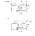
- FIG. 1 is a sectional view depicting a manufacturing method of an electronic component-embedded substrate relating to preliminary matters (1 thereof).
- FIGS. 2A and 2B are a sectional view and a plan view depicting the manufacturing method of the electronic component-embedded substrate relating to the preliminary matters (2 thereof).
- FIG. 3 is a sectional view depicting the manufacturing method of the electronic component-embedded substrate relating to the preliminary matters (3 thereof).
- FIGS. 4A and 4B are a sectional view and a plan view depicting the manufacturing method of the electronic component-embedded substrate relating to the preliminary matters (4 thereof).
- FIG. 5 is a sectional view depicting the manufacturing method of the electronic component-embedded substrate relating to the preliminary matters (5 thereof).
- FIG. 6 is a sectional view depicting the manufacturing method of the electronic component-embedded substrate relating to the preliminary matters (6 thereof).
- FIG. 7 is a sectional view depicting the manufacturing method of the electronic component-embedded substrate relating to the preliminary matters (7 thereof).
- FIG. 8 is a sectional view depicting the manufacturing method of the electronic component-embedded substrate relating to the preliminary matters (8 thereof).
- FIG. 9 is a sectional view depicting the manufacturing method of the electronic component-embedded substrate relating to the preliminary matters (9 thereof).
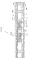
- FIGS. 10A and 10B are plan views for illustrating a problem of the manufacturing method of the electronic component-embedded substrate relating to the preliminary matters.
- FIGS. 11A and 11B are a sectional view and a partial plan view depicting a manufacturing method of an electronic component-embedded substrate according to an exemplary embodiment (1 thereof).
- FIGS. 12A to 12D are sectional views depicting the manufacturing method of the electronic component-embedded substrate according to the exemplary embodiment (2 thereof).
- FIGS. 13A and 13B are a sectional view and a plan view depicting the manufacturing method of the electronic component-embedded substrate according to the exemplary embodiment (3 thereof).
- FIG. 14 is a sectional view depicting the manufacturing method of the electronic component-embedded substrate according to the exemplary embodiment (4 thereof).
- FIGS. 15A and 15B are a sectional view and a plan view depicting the manufacturing method of the electronic component-embedded substrate according to the exemplary embodiment (5 thereof).
- FIG. 16 is a sectional view depicting the manufacturing method of the electronic component-embedded substrate according to the exemplary embodiment (6 thereof).
- FIG. 17 is a sectional view depicting the manufacturing method of the electronic component-embedded substrate according to the exemplary embodiment (7 thereof).
- FIG. 18 is a sectional view depicting the manufacturing method of the electronic component-embedded substrate according to the exemplary embodiment (8 thereof).
- FIG. 19 is a sectional view depicting the manufacturing method of the electronic component-embedded substrate according to the exemplary embodiment (9 thereof).
- FIG. 20 is a sectional view depicting the manufacturing method of the electronic component-embedded substrate according to the exemplary embodiment (10 thereof).
- FIGS. 21A to 21C are sectional views depicting a method of forming a second wiring layer of FIG. 20 (11 thereof).
- FIGS. 22A and 22B are sectional views depicting the method of forming the second wiring layer of FIG. 20 (12 thereof).
- FIG. 23 is a sectional view depicting an electronic component-embedded substrate according to the exemplary embodiment.
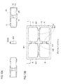
- FIGS. 24A to 24C are a plan view and a sectional view depicting a structure around a cavity of the electronic component-embedded substrate shown in FIG. 23 and an aspect of capacitors arranged in the cavity.
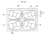
- FIG. 25 is a plan view depicting an aspect where four electronic components of the electronic component-embedded substrate shown in FIG. 23 are arranged with being out of alignment.
- FIG. 26 is a plan view depicting an electronic component-embedded substrate according to a first modified embodiment of the exemplary embodiment.
- FIG. 27 is a plan view depicting an electronic component-embedded substrate according to a second modified embodiment of the exemplary embodiment.
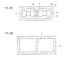
- FIGS. 28A and 28B are plan views depicting a structure around the cavity in a case where two electronic components are mounted to the electronic component-embedded substrate.
- FIG. 29 is a sectional view depicting an electronic component device of the exemplary embodiment.
- preliminary matters which are bases of the present invention, are first described. It should be noted that the preliminary matters relate to personal investigation contents of the inventors and include a novel technology, not a known technology.
- FIGS. 1 to 10B illustrate a manufacturing method of an electronic component-embedded substrate relating to the preliminary matters.
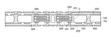
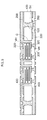
- a core substrate 100 having a structure as shown in FIG. 1 is first prepared. Both surfaces of the core substrate 100 are formed with first wiring layers 200 , respectively.
- the core substrate 100 is formed with through-holes TH, the first wiring layers 200 on both the surfaces are connected to each other via through-conductors 120 in the through-holes TH.
- a cavity formation area A is defined. Both surfaces of the cavity formation area. A of the core substrate 100 are not formed with the first wiring layer 200 , and are configured as a collective opening.
- the cavity formation area A of the core substrate 100 is subjected to laser processing to form a cavity C penetrating in a thickness direction.
- insulation wall portions W having a projection shape are respectively formed at central portions of a pair of sidewalls facing each other in a longitudinal direction of the cavity C.
- the insulation wall portion W is arranged as a portion of the core substrate 100 is left on the sidewall of the cavity C.
- An inside of the cavity C is divided into two component embedding areas by the insulation wall portions W, and capacitors are respectively mounted in the two component embedding areas.
- the insulation wall portions W are provided so as to prevent an electric short, which is caused due to contact of connection terminals of the adjacent capacitors when mounting the two capacitors.
- a temporary fixing tape 140 is bonded to an upper surface of the core substrate 100 .
- capacitors 300 each of which has connection terminals 320 provided at both ends thereof are prepared, and upper surfaces of the capacitors 300 are bonded to the temporary fixing tape 140 in the cavity C of the core substrate 100 .
- the capacitors 300 are respectively arranged in the two component embedding areas in the cavity C of the core substrate 100 .
- a resin film is stacked on a lower surface of the core substrate 100 , so that a first insulation layer 400 is formed. Thereby, side surfaces and lower surfaces of the capacitors 300 are sealed by the first insulation layer 400 .
- the temporary fixing tape 140 is peeled off from the core substrate 100 , so that the upper surfaces of the core substrate 100 and the capacitors 300 are exposed.
- a resin film is stacked on the upper surface of the core substrate 100 , so that a second insulation layer 420 is formed. Thereby, the upper surfaces of the capacitors 300 are sealed by the second insulation layer 420 .
- the first insulation layer 400 formed on the lower surface of the core substrate 100 is subjected to the laser processing to form via-holes VH that reach the lower surfaces of the connection terminals 320 of the capacitors 300 and the first wiring layer 200 .
- the second insulation layer 420 formed on the upper surface of the core substrate 100 is subjected to the laser processing to form via-holes VH that reach the upper surfaces of the connection terminals 320 of the capacitors 300 and the first wiring layer 200 .
- second wiring layers 220 are respectively formed on the first insulation layer 400 and the second insulation layer 420 .
- the second wiring layer 220 on the first insulation layer 400 is connected to the lower surfaces of the connection terminals 320 of the capacitors 300 and the first wiring layer 200 through the via-holes VH.
- the second wiring layer 220 on the second insulation layer 420 is connected to the upper surfaces of the connection terminals 320 of the capacitors 300 and the first wiring layer 200 through the via-holes VH.
- the two capacitors 300 are mounted side by side in a lateral direction. In this case, even when the two capacitors 300 are mounted with being rotated and inclined, the connection electrodes 320 of the two capacitors 300 are prevented from contacting each other by the insulation wall portions W arranged therebetween.
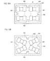
- FIGS. 10A and 10B depict an aspect where the four capacitors are mounted in the cavity C of the core substrate 100 .
- first insulation wall portions W 1 having a projection shape are respectively formed at central portions of a pair of sidewalls of the cavity C facing each other in the lateral direction.
- second insulation wall portions W 2 having a projection shape are respectively formed at central portions of a pair of sidewalls of the cavity C facing each other in the longitudinal direction.
- connection terminals 320 of the capacitors 300 adjacent to each other in the longitudinal direction are contacted, so that an electric short may be caused.
- the first insulation wall portions W 1 and the second insulation wall portions W 2 may be extended so that the insulation wall portions are arranged up to the area B of FIG. 10A .
- the insulation wall portion only by the core substrate 100 , it is not possible to secure the sufficient strength when the wall thickness of the insulation wall portion is reduced. Therefore, when mounting the capacitors or when sealing the capacitors with the resin, the insulation wall portion may be damaged, so that it is not possible to reliably arrange the insulation wall portion.
- FIGS. 11A to 22B illustrate a manufacturing method of an electronic component-embedded substrate of an exemplary embodiment
- FIGS. 23 to 28B illustrate an electronic component-embedded substrate of the exemplary embodiment
- FIG. 29 depicts an electronic component device of the exemplary embodiment.
- a core substrate 10 having a structure as shown in FIG. 11A is first prepared.
- the core substrate 10 is formed of an insulating material such as an epoxy resin having glass cloth inserted therein.
- Both surfaces of the core substrate 10 are formed with first wiring layers 20 , respectively.
- the core substrate 10 is formed with through-holes TEL penetrating in a thickness direction.
- the first wiring layers 20 on both the surfaces are connected to each other by means of through-conductors 12 formed in the through-holes TH.
- a thickness of the core substrate 10 is 60 ⁇ m to 500 ⁇ m, for example.
- a through-hole plating layer may be formed on an inner wall of the through-hole TH of the core substrate 10 and the remaining portion of the through-hole TH may be filled with a resin.
- the first wiring layers 20 on both the surfaces are connected to each other by the through-hole plating layer.
- the through-hole TH is formed by a drill or laser.
- the first wiring layer 20 and the through-conductor 12 are made of copper or the like, and are formed using photolithography, plating, wet-etching and the like.
- one surface of the core substrate 10 is set as an upper surface, and the other surface is set as a lower surface.
- a cavity formation area A in which a cavity is to be arranged is defined.
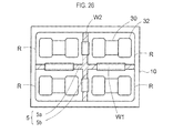
- an aspect where four electronic components are mounted side by side in the cavity is exemplified.
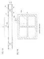
- a cross-shaped support pattern 5 is arranged in the rectangular cavity formation area A of the upper surface of the core substrate 10 , and four openings 20 a of the support pattern 5 are arranged in the cavity formation area A.
- the support pattern 5 is configured by a lateral pattern 5 a and a longitudinal pattern 5 b intersecting with each other.
- the support pattern 5 is arranged to extend over the cavity formation area A in a lateral direction and a longitudinal direction.
- the lateral and longitudinal end portions of the support pattern 5 are coupled and supported to a ring-shaped conductor layer 21 .
- the first wiling layer 20 , the support pattern 5 and the conductor layer 21 are patterned and formed at the same time by performing photolithography and etching for a metal layer made of copper, aluminum or the like. In this way, the support pattern 5 and the conductor layer 21 are formed by the same layer as the first wiring layer 20 .
- the first wiring layer 20 is an electric wiring for establishing an electric circuit.
- the support pattern 5 and the conductor layer 21 are electrically insulated from the first wiring layer 20 , and are formed as floating conductors. Alternatively, the support pattern 5 may be electrically connected to the first wiring layer 20 .
- a lower surface of the cavity formation area A of the core substrate 10 is not formed with the first wiring layer 20 , and the cavity formation area A is entirely configured as an opening 20 b.
- the core substrate 10 is first formed with four cavities so as to correspond to the four openings 20 a of the support pattern 5 .
- the laser processing is performed from an opposite surface to the surface of the core substrate 10 on which the support pattern 5 is formed.
- the laser processing is performed from the lower surface of the core substrate 10 .
- the core substrate 10 is sequentially subjected to the laser processing along portions becoming sidewalls of the four cavities, so that the unnecessary portions of the core substrate 10 are removed.
- FIG. 12B thereby, as shown in FIG. 12B , four component embedding areas R, which are through-holes corresponding to the four openings 20 a of the support pattern 5 , are formed. At the same time, a cross-shaped wall plate Wx consisting of a part of the core substrate 10 is arranged on the cross-shaped support pattern 5 ( FIG. 11B ).
- a width of the wall plate Wx is set greater than a width of the support pattern 5 .
- the cross-shaped wall plate Wx is configured by a lateral pattern P 1 and a longitudinal pattern P 2 intersecting with each other.
- a of the core substrate 10 may be formed with the four similar component embedding areas R by using a laser device capable of collectively processing a predetermined surface area by laser illumination.
- a plurality of component embedding areas R penetrating the core substrate 10 is formed at positions facing each other with the support pattern 5 ( FIG. 11B ) being interposed therebetween, as seen from a plan view.
- central portions of the lateral pattern P 1 arranged at both sides of the longitudinal pattern P 2 of the cross-shaped wall plate Wx are subjected to the laser processing. Also, likewise, central portions of the longitudinal pattern P 2 arranged at both sides of the lateral pattern P 1 of the cross-shaped wall plate Wx are subjected to the laser processing.
- first openings 11 a are respectively formed at the central portions of the lateral pattern P 1 arranged at both sides of the longitudinal pattern P 2 .
- second openings 11 b are respectively formed at the central portions of the longitudinal pattern P 2 arranged at both sides of the lateral pattern P 1 .
- the support pattern 5 remains as it is not damaged by the laser, and only the unnecessary portions of the wall plate Wx are removed.
- the cross-shaped wall plate Wx is formed with the first openings 11 a and the second openings 11 b , so that the four component embedding areas R partitioned by the cross-shaped wall plate Wx are coupled to form one integral cavity C.
- the cross-shaped wall plate Wx is patterned, so that the first insulation wall portions W 1 are respectively arranged at four end portions of the cross-shaped support pattern 5 .
- the first insulation wall portion W 1 is coupled to the core substrate 10 of the sidewall of the cavity C, so that it has a projection shape.
- a cross-shaped second insulation wall portion W 2 is arranged at an intersection portion of the cross-shaped support pattern 5 .
- the cross-shaped second insulation wall portion W 2 is formed with being separated from the core substrate 10 .
- the cavity C is divided into the four component embedding areas R by the support pattern 5 , as seen from a plan view.
- the first and second insulation wall portions W 1 , W 2 made of the same material as the core substrate 10 are formed on the support pattern 5 .
- the four component embedding areas R are defined in the cavity C by the support pattern 5 .
- the support pattern 5 having a lattice shape may be formed by intersecting a plurality of lateral patterns 5 a and a plurality of longitudinal patterns 5 b.
- the first insulation wall portions WI and the second insulation wall portion W 2 are divided and formed on the inner surface of the support pattern 5 in the cavity C of the core substrate 10 .
- FIG. 13B is a partial plan view of a structure around the cavity C of a sectional view of FIG. 13A , as seen from below.
- C is a sectional view taken along a line I-I of FIG. 13B .
- the support pattern 5 is arranged to extend over the cavity C. Also, at the same time, the first insulation wall portions W 1 and the second insulation wall portion W 2 made of the same material as the core substrate 10 are arranged on the inner surface of the support pattern 5 . In addition, at the same time, the plurality of component embedding areas R is defined in the cavity C by the support pattern 5 , as seen from a plan view.
- the insulation wall portion is formed on the support pattern 5 , it is possible to separate the insulation wall portion from the core substrate 10 and to arrange the same at any position on the support pattern 5 . Also, since the insulation wall portion is reinforced by the support pattern 5 , the sufficient strength is secured even though the wall thickness of the insulation wall portion is reduced.
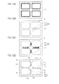
- capacitors 30 are prepared.
- the capacitor 30 shown in FIG. 15A is a stacked ceramic chip capacitor where a dielectric layer 34 and an internal electrode 36 are stacked in a multi-layer structure.
- the capacitor 30 has connection terminals 32 at both horizontal ends, and the connection terminal 32 is connected to one end of the stacked internal electrode 36 .
- connection terminals 32 provided at both ends of the capacitor 30 are formed to cover a capacitor main body from an upper surface end portion to a lower surface end portion, respectively, and the wiring layer can be connected to the upper surface and the lower surface of the connection terminal 32 .
- the capacitor 30 is an example of the electronic component.
- the upper surface of the capacitor 30 is bonded to the temporary fixing tape 17 in the cavity C of the core substrate 10 .
- the capacitors 30 are respectively mounted in the four component embedding areas It in the cavity C of the core substrate 10 .
- an uncured resin film is stacked on a lower surface of the structure of FIG. 15A by hot press, and the resin film is cured by heating, so that a first insulation layer 40 is formed.
- the cavity C of the lower surface of the core substrate 10 is filled, so that the first insulation layer 40 covering the side surfaces and lower surfaces of the capacitors 30 is formed. Also, the side surfaces of the first insulation wall portions W 1 and the second insulation wall portion W 2 are covered by the first insulation layer 40 .
- the temporary fixing tape 17 is peeled off from the core substrate 10 , so that the upper surfaces of the core substrate 10 and the capacitors 30 are exposed.
- an uncured resin film is stacked on an upper surface of the structure of FIG. 17 by hot press, and the resin film is cured by heating, so that a second insulation layer 42 is formed.
- the upper surface of the core substrate 10 is formed with the second insulation layer 42 covering the upper surfaces of the capacitors 30 .
- an insulating resin such as epoxy resin, polyimide resin or the like is used as the first insulation layer 40 and the second insulation layer 42 . In this way, the cavity C is filled with the insulating material.
- the first insulation layer 40 formed on the lower surface of the core substrate 10 is subjected to the laser processing to form first via-holes VH 1 that reach the lower surfaces of the connection terminals 32 of the capacitors 30 and the first wiring layer 20 .
- the second insulation layer 42 formed on the upper surface of the core substrate 10 is subjected to the laser processing to form second via-holes VH 2 that reach the upper surfaces of the connection terminals 32 of the capacitors 30 and the first wiring layer 20 .
- a second wiring layer 22 is formed on the first insulation layer 40 on the lower surface of the core substrate 10 .
- the second wiring layer 22 is connected to the lower surfaces of the connection terminals 32 of the capacitors 30 and the first wiring layer 20 through the first via-holes VH 1 .
- a third wiring layer 24 is formed on the second insulation layer 42 on the upper surface of the core substrate 10 .
- the third wiring layer 24 is connected to the upper surfaces of the connection terminals 32 of the capacitors 30 and the first wiring layer 20 through the second via-holes VH 2 .
- the second wiring layer 22 and the third wiring layer 24 are formed by a semi-additive method. In the below, a method of forming the third wiring layer 24 is described in detail.
- FIG. 21A is a partially enlarged view of a surrounding of the second via-hole VH 2 on the left connection terminal 32 of the capacitor 30 of FIG. 19 .
- an inside of the second via-hole VH 2 is subjected to desmear processing by using permanganic acid or the like, so that the resin smear in the second via-hole VH 2 is removed and the second via-hold is thus cleaned.
- an inner wall of the second via-hole VH 2 and the second insulation layer 42 are formed thereon with a seed layer 24 a by an electroless plating method or a sputtering method.
- a metal plated layer 24 b is formed to fill the second via-hole VH 2 and the opening 43 a of the plated resist layer 43 by an electrolytic plating method in which the seed layer 24 a is used as a plating power feeding path.
- the seed layer 24 a and the metal plated layer 24 b are formed of copper or the like.
- the seed layer 24 a is etched using the metal plated layer 24 b as a mask.
- the third wiring layer 24 is formed from the seed layer 24 a and the metal plated layer 24 b.
- the second wiring layer 22 and the third wiring layer 24 may be formed by a MSAP (Modified Semi Additive Process) or a subtractive method.
- solder resist layer 44 having openings 44 a formed on connection portions of the second wiring layer 22 is formed on the first insulation layer 40 of FIG. 20
- solder resist layer 46 having openings 46 a formed on connection portions of the third wiring layer 24 is formed on the second insulation layer 42 of FIG. 20 .
- an electronic component-embedded substrate 1 of the exemplary embodiment is manufactured.
- the electronic component-embedded substrate 1 of the exemplary embodiment has the core substrate 10 having the structure shown in FIG. 11A at a central part in a thickness direction thereof.
- the first wiring layers 20 are respectively formed on both surfaces of the core substrate 10 .
- the first wiring layers 20 on both surfaces are connected to each other by means of the through-conductors 12 formed in the through-holes TH of the core substrate 10 .
- the core substrate 10 is formed with the cavity C penetrating the core substrate in the thickness direction.
- One surface of the core substrate 10 is formed with the support pattern 5 made of the same layer as the first wiring layer 20 .
- the cavity C is divided into the four component embedding areas R by the support pattern 5 , as seen from a plan view.
- the capacitors 30 are respectively mounted in the four component embedding areas R of the cavity C.
- the lower surface of the core substrate 10 is formed with the first insulation layer 40 , and the side surfaces and lower surfaces of the capacitors 30 and the first wiring layer 20 are covered with the first insulation layer 40 .
- the first insulation layer 40 is filled between the inner wall of the cavity C of the core substrate 10 and the side surface of each capacitor 30 . Also, the first insulation layer 40 is filled between the four capacitors 30 . In this way, the first insulation layer 40 (insulating material) fills the inside of the cavity C.
- the upper surface of the core substrate 10 is formed thereon with the second insulation layer 42 .
- the upper surfaces of the capacitors 30 and the first wiring layer 20 are covered with the second insulation layer 42 .
- the first insulation layer 40 is formed with the first via-holes VH 1 that reach the lower surfaces of the connection electrodes 32 of the capacitors 30 and the first wiring layer 20 provided at the lower side of the core substrate 10 .
- the first insulation layer 40 is formed thereon with the second wiring layer 22 .
- the second wiring layer 22 is connected to the lower surfaces of the connection electrodes 32 of the capacitors 30 and the first wiring layer 20 through the via conductors in the first via-holes VH 1 .
- the second insulation layer 42 is formed with the second via-holes VH 2 that reach the upper surfaces of the connection electrodes 32 of the capacitors 30 and the first wiring layer 20 provided at the upper side of the core substrate 10 .
- the second insulation layer 42 is formed thereon with the third wiring layer 24 .
- the third wiring layer 24 is connected to the upper surfaces of the connection electrodes 32 of the capacitors 30 and the first wiring layer 20 through the via conductors in the second via-holes VH 2 .
- solder resist layer 44 having the openings 44 a formed on the connection portions of the second wiring layer 22 is formed on the first insulation layer 40 .
- solder resist layer 46 having the openings 46 a formed on the connection portions of the third wiring layer 24 is formed on the second insulation layer 42 .
- the two wiring layers are respectively stacked on both the surfaces of the core substrate 10 .
- the number of the wiring layers to be stacked on both the surfaces of the core substrate 10 may be arbitrarily set.
- FIG. 24A is a partial plan view depicting an aspect of the four capacitors arranged in the cavity C of FIG. 23 , as seen from below.
- FIG. 24B is a plan view depicting only the support pattern 5 of FIG. 24A , as seen from back.
- FIG. 24C is a sectional view taken along a line II-II of FIG. 24A .
- the cross-shaped support pattern 5 is arranged in the cavity C of the core substrate 10 , as seen from a plan view.
- the cross-shaped support pattern 5 is arranged to extend over the cavity C in the lateral and longitudinal directions.
- the cross-shaped support pattern 5 is configured by the lateral pattern 5 a and the longitudinal pattern 5 b intersecting with each other. Both ends of each of the lateral pattern 5 a and the longitudinal pattern 5 b of the support pattern 5 are coupled and supported to the ring-shaped conductor layer 21 formed on the upper surface of the core substrate 10 .
- the first insulation wall portions W 1 having a projection shape protruding inward from the sidewalls of the cavity C are formed on both end portions of the lateral pattern 5 a and the longitudinal pattern 5 b of the cross-shaped support pattern 5 .
- the first insulation wall portions W 1 are formed with being coupled to the core substrate 10 .
- the first insulation wall portions W 1 are arranged as protruding wall portions protruding from the core substrate 10 towards the inside of the cavity C.
- the support pattern 5 has an intersection part at which the band-shaped lateral pattern 5 a and the band-shaped longitudinal pattern 5 b intersect with each other.
- the second insulation wall portion W 2 is arranged as a cross-shaped wall portion on the intersection part of the lateral pattern 5 a and the longitudinal pattern 5 b.
- the second insulation wall portion W 2 is arranged with being separated from the core substrate 10 .
- the first insulation wall portions W 1 and the second insulation wall portion W 2 are arranged on the inner surface of the support pattern 5 facing towards the cavity C.
- the first openings 11 a are formed between the two first insulation wall portions W 1 facing each other in the lateral direction and the lateral pattern of the cross-shaped second insulation wall portion W 2 . Also, the second openings 11 b are formed between the two first insulation wall portions W 1 facing each other in the longitudinal direction and the longitudinal pattern of the cross-shaped second insulation wall portion W 2 .
- first insulation wall portions W 1 and the second insulation wall portion W 2 are arranged with being separated from each other.
- the insulation wall portions may be arranged at portions on the support pattern in the cavity.
- the four component embedding areas R are defined in the cavity C by the cross-shaped support pattern 5 , as seen from a plan view.
- the four component embedding areas R are coupled by the first openings 11 a and the second openings 11 b, so that one collective cavity C is established.
- the first insulation wall portions W 1 and the second insulation wall portion W 2 are arranged as portions of the core substrate 10 are left on the inner surface of the support pattern 5 when forming the cavity C by laser processing the core substrate 10 . Therefore, the first insulation wall portions W 1 and the second insulation wall portion W 2 are made of the same material as the core substrate 10 .
- the capacitors 30 are respectively arranged in the four component embedding areas R in the cavity C. In this way, the four capacitors 30 are arranged in the cavity C.
- the first insulation wall portions W 1 and the second insulation wall portion W 2 are arranged on the inner surface of the support pattern 5 between the plurality of capacitors 30 .
- the cross-shaped support pattern 5 is arranged to extend over the cavity C on one surface of the core substrate 10 , and the first insulation wall portions W 1 and the second insulation wall portion W 2 are arranged on the inner surface of the support pattern 5 .
- the support pattern 5 functions as a support body for supporting the first insulation wall portions WI and the second insulation wall portion W 2 .
- the first insulation wall portions W 1 are arranged as a projection shape on both end portions of the lateral pattern 5 a and the longitudinal pattern 5 b of the cross-shaped support pattern 5 with being coupled to the core substrate 10 .
- the support pattern 5 is used as the support body, so that the cross-shaped second insulation wall portion W 2 can be arranged in an area, to which the connection terminals 32 of the four capacitors 30 are adjacent, with being separated from the core substrate 10 .
- connection electrodes 32 of the capacitors 30 are prevented from contacting each other.
- connection electrodes 32 of the capacitors 30 adjacent to each other are contacted to the first insulation wall portions W 1 and the second insulation wall portion W 2 , so that the electric short between the capacitors 30 is prevented.
- the insulation wall portion is formed on the support pattern 5 functioning as a support body. Therefore, the insulation wall portion can be arranged at any position on the support pattern 5 with being separated from the core substrate 10 .
- the insulation wall portion is reinforced by the support pattern 5 , so that the sufficient strength is secured.
- the insulation wall portion is set to be small, when mounting the capacitors or when sealing the capacitors with the resin, the insulation wall portion is prevented from being damaged, so that the insulation wall portion can be reliably arranged.
- a width WA of the second insulation wall portion W 2 is set greater than a width WB of the support pattern 5 .
- a width of the first insulation wall portion W 1 is set greater than the width of the support pattern 5 .
- connection electrode 32 of the capacitor 30 is contacted to the first insulation wall portion W 1 and the second insulation wall portion W 2 , it is not contacted to the support pattern 5 . Therefore, since it is possible to prevent the electric short between the capacitors 30 , it is possible to improve the mounting density by narrowing the arrangement pitch of the plurality of capacitors 30 .
- a height of the second insulation wall portion W 2 is set to be the same as the thickness of the core substrate 10 .
- the height of the second insulation wall portion W 2 may be set lower than the thickness of the core substrate 10 .
- a height of the first insulation wall portion W 1 is also the same.
- the second insulation wall portion W 2 is not provided in the area (the central portion of the cavity C 1 to which the four capacitors 30 are adjacent, it is difficult to fill the resin in the corresponding area, so that the first insulation layer 40 may be formed into a concave shape.
- the insulation wall portion in any area, in which it is difficult to fill the resin, of the areas between the plurality of capacitors 30 .
- the insulation wall portion is arranged on the support pattern 5 , so that it is possible to prevent the electric short between the plurality of capacitors 30 and to arrange the insulation wall portion at the optimal position at which the resin is favorably filled.
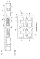
- FIG. 26 depicts a first modified embodiment of the exemplary embodiment.
- the cavity C is divided into the four component embedding areas R by the cross-shaped support pattern 5 .
- the capacitors 30 are respectively arranged in the four component embedding areas R in the cavity C.
- the first insulation wall portions W 1 are respectively arranged at the central portions of the lateral pattern 5 a at both sides of the longitudinal pattern 5 b of the support pattern 5 .
- the first insulation wall portions W 1 are arranged with being separated from the core substrate 10 .
- the first insulation wall portion W 1 is arranged to extend in the lengthwise direction so that both end portions thereof are arranged between both the connection electrodes 32 of the capacitors 30 adjacent to each other in the longitudinal direction.
- the second insulation wall portions W 2 are respectively arranged at the central portions of the longitudinal pattern 5 b at both sides of the lateral pattern 5 a of the support pattern 5 .
- the second insulation wall portions W 2 are arranged with being separated from the core substrate 10 .
- the second insulation wall portion W 2 is arranged between the connection electrodes 32 of the capacitors 30 adjacent to each other in the lateral direction.
- connection electrodes 32 of the capacitors 30 are prevented from contacting each other.
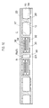
- FIG. 27 depicts a second modified embodiment of the exemplary embodiment.
- the two first insulation wall portions W 1 are arranged with being separated on the lateral pattern 5 a. of each of both sides of the longitudinal pattern 5 b of the support pattern 5 .
- the first insulation wall portion W 1 is arranged with being separated from the core substrate 10 .
- the first insulation wall portions W 1 are arranged with being separated between both the connection electrodes 32 of the capacitors 30 adjacent to each other in the longitudinal direction.
- the second insulation wall portions W 2 are respectively arranged at the central portions of the longitudinal pattern 5 b at both sides of the lateral pattern 5 a of the support pattern 5 .
- connection electrodes 32 of the capacitors 30 are prevented from contacting each other.
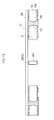
- FIG. 28A is a partial plan view depicting a structure around the cavity of the electronic component-embedded substrate when mounting the two capacitors.
- FIG. 28B is a partial plan view depicting the support pattern when mounting the two capacitors.
- the two capacitors are arranged side by side in the lateral direction.
- the support pattern 5 is arranged to extend over the cavity C in the longitudinal direction, and is coupled and supported to the ring-shaped. conductor layer 21 arranged on the core substrate 10 .
- the support pattern 5 has a band shape narrower than an opening width of the cavity C.
- the insulation wall portions W having a projection shape protruding inward from the sidewalls of the cavity C are arranged on the inner surfaces of both end portions of the support pattern 5 .
- the insulation wall portions W are arranged on the support pattern 5 , so that the sufficient strength can be secured even though the wall thickness of the insulation wall portion W is thinned to extend the protruding length thereof. Also, the insulation wall portion W can be arranged at any position with being separated from the core substrate 10 .
- the two capacitors may be arranged side by side in the longitudinal direction.
- the band-shaped support pattern is arranged between the two capacitors, and the insulation wall portion is arranged at any position of the inner surface of the support pattern.
- the support pattern 5 having a lattice shape may be arranged in the cavity C of the core substrate 10 to divide the inside of the cavity C into the arbitrary number of the component embedding areas R, and the arbitrary number of the capacitors 30 may be mounted therein.
- the insulation wall portion is arranged at a position between the capacitors 30 so that the electric short is not to occur between the capacitors 30 .
- the band-shaped the support pattern 5 may be simultaneously formed and used as the component mounting pattern in the respective component embedding areas R of the cavity C, to which the capacitors 30 are to be arranged.
- the temporary fixing tape 17 is not used and the capacitors 30 are fixed to the inner surface of the component mounting pattern by an adhesive.
- FIG. 29 depicts an electronic component device 2 for which the electronic component-embedded substrate 1 of FIG. 23 is used.
- pads of a semiconductor chip 50 are flip-chip connected to the connection portions of the third wiring layer 24 provided on the upper surface-side of the electronic component-embedded substrate 1 of FIG. 23 by bump electrodes 52 such as solders.
- the semiconductor chip 50 is electrically connected to the capacitors 30 via the third wiring layer 24 and the first wiring layer 20 .
- connection portions of the second wiring layer 22 provided on the lower surface-side of the electronic component-embedded substrate 1 are provided with external connection terminals T such as solder balls.
- the capacitors 30 embedded in the electronic component-embedded substrate 1 function as decoupling capacitors arranged between a power supply line and a ground line of the semiconductor chip 50 .
- the decoupling capacitor is used so as to stabilize a power supply voltage and to reduce a high-frequency noise.
- the plurality of component embedding areas R is defined in the cavity C.
- the capacitors 30 are respectively arranged in the plurality of component embedding areas R in the cavity C.
- a manufacturing method of an electronic component-embedded substrate comprising:
Landscapes
- Engineering & Computer Science (AREA)
- Microelectronics & Electronic Packaging (AREA)
- Manufacturing & Machinery (AREA)
- Production Of Multi-Layered Print Wiring Board (AREA)
- Physics & Mathematics (AREA)
- Geometry (AREA)
Abstract
Description
- The present application claims priority from Japanese Patent Application No. 2016-196164 tiled on Oct. 4, 2016, the entire content of which is incorporated herein by reference.
- The present invention relates to an electronic component-embedded substrate and an electronic component device.
- In the related art, an electronic component-embedded substrate in which electronic components such as semiconductor chips, capacitors and the like are embedded has been known. In the electronic component-embedded substrate, the electronic components are arranged in a cavity formed in a core substrate, and a wiring layer is connected to the electronic components.
- Patent Document 1:WO2012/157426
- As described later in paragraphs of preliminary matters, when mounting a plurality of capacitors in the cavity of the core substrate, connection terminals of the capacitors are contacted to each other in an area to which the plurality of capacitors is respectively adjacent, so that an electric short may be caused.
- Exemplary embodiments of the invention provide an electronic component-embedded substrate having a novel structure capable of reliably mounting a plurality of electronic components in a cavity of a core substrate, and an electronic component device.
- An electronic component-embedded substrate according to an exemplary embodiment, comprises:
- a core substrate;
- a cavity penetrating the core substrate;
- a wiring layer formed on one surface of the core substrate;
- a support pattern extending over the cavity and configured to divide the cavity into a plurality of component embedding areas;
- an insulation wall portion arranged on a part of the support pattern in the cavity and formed of the same material as the core substrate;
- a plurality of electronic components each of which is mounted in each of the plurality of component embedding areas; and
- an insulating material filling an inside of the cavity.
- The support pattern may be formed of the same layer as the wiring layer.
- A manufacturing method of an electronic component-embedded substrate, according to an exemplary embodiment, the method comprises;
- preparing a core substrate;
- forming a wiring layer and a support pattern formed of the same layer as the wiring layer on one surface of the core substrate;
- forming a plurality of component embedding areas penetrating the core substrate at positions at which the component embedding areas face each other with the support pattern being interposed therebetween;
- forming one cavity, in which the plurality of component embedding areas is coupled, and forming an insulation wall portion formed of the same material as the core substrate on the support pattern by removing a portion of the core substrate positioned on the support pattern between the plurality of component embedding areas;
- mounting each of electronic components in each of the plurality of component embedding areas; and
- filling an inside of the cavity with an insulating material.
- According to the following present invention, the core substrate of the electronic component-embedded substrate is formed with the cavity penetrating in a thickness direction. One surface of the core substrate is formed with the support pattern formed of the same layer as the wiring layer over the cavity.
- The inside of the cavity is divided into the plurality of component embedding areas by the support pattern. Also, the insulation wall portion formed of the same material as the core substrate is arranged on the inner surface of the support pattern.
- In the plurality of component embedding areas, the electronic components are respectively arranged, and the insulation wall portion is arranged between the plurality of electronic components.
- Thereby, when mounting the plurality of electronic components, for example, the electronic components are prevented from contacting each other by the insulation wall portion even though the electronic components are inclined or positionally deviated.
- Also, since the insulation wall portion is arranged on the support pattern, it is possible to arrange the insulation wall portion at any position on the inner surface of the support pattern with being separated from the core substrate.
- Thereby, for example, even when mounting the four electronic components in a two-row and two-column form in the cavity of the core substrate, the insulation wall portion can be arranged even at the central portion of the cavity to which the four electronic components are adjacent, so that the electric short between the electronic components is prevented.
-
FIG. 1 is a sectional view depicting a manufacturing method of an electronic component-embedded substrate relating to preliminary matters (1 thereof). -
FIGS. 2A and 2B are a sectional view and a plan view depicting the manufacturing method of the electronic component-embedded substrate relating to the preliminary matters (2 thereof). -
FIG. 3 is a sectional view depicting the manufacturing method of the electronic component-embedded substrate relating to the preliminary matters (3 thereof). -
FIGS. 4A and 4B are a sectional view and a plan view depicting the manufacturing method of the electronic component-embedded substrate relating to the preliminary matters (4 thereof). -
FIG. 5 is a sectional view depicting the manufacturing method of the electronic component-embedded substrate relating to the preliminary matters (5 thereof). -
FIG. 6 is a sectional view depicting the manufacturing method of the electronic component-embedded substrate relating to the preliminary matters (6 thereof). -
FIG. 7 is a sectional view depicting the manufacturing method of the electronic component-embedded substrate relating to the preliminary matters (7 thereof). -
FIG. 8 is a sectional view depicting the manufacturing method of the electronic component-embedded substrate relating to the preliminary matters (8 thereof). -
FIG. 9 is a sectional view depicting the manufacturing method of the electronic component-embedded substrate relating to the preliminary matters (9 thereof). -
FIGS. 10A and 10B are plan views for illustrating a problem of the manufacturing method of the electronic component-embedded substrate relating to the preliminary matters. -
FIGS. 11A and 11B are a sectional view and a partial plan view depicting a manufacturing method of an electronic component-embedded substrate according to an exemplary embodiment (1 thereof). -
FIGS. 12A to 12D are sectional views depicting the manufacturing method of the electronic component-embedded substrate according to the exemplary embodiment (2 thereof). -
FIGS. 13A and 13B are a sectional view and a plan view depicting the manufacturing method of the electronic component-embedded substrate according to the exemplary embodiment (3 thereof). -
FIG. 14 is a sectional view depicting the manufacturing method of the electronic component-embedded substrate according to the exemplary embodiment (4 thereof). -
FIGS. 15A and 15B are a sectional view and a plan view depicting the manufacturing method of the electronic component-embedded substrate according to the exemplary embodiment (5 thereof). -
FIG. 16 is a sectional view depicting the manufacturing method of the electronic component-embedded substrate according to the exemplary embodiment (6 thereof). -
FIG. 17 is a sectional view depicting the manufacturing method of the electronic component-embedded substrate according to the exemplary embodiment (7 thereof). -
FIG. 18 is a sectional view depicting the manufacturing method of the electronic component-embedded substrate according to the exemplary embodiment (8 thereof). -
FIG. 19 is a sectional view depicting the manufacturing method of the electronic component-embedded substrate according to the exemplary embodiment (9 thereof). -
FIG. 20 is a sectional view depicting the manufacturing method of the electronic component-embedded substrate according to the exemplary embodiment (10 thereof). -
FIGS. 21A to 21C are sectional views depicting a method of forming a second wiring layer ofFIG. 20 (11 thereof). -
FIGS. 22A and 22B are sectional views depicting the method of forming the second wiring layer ofFIG. 20 (12 thereof). -
FIG. 23 is a sectional view depicting an electronic component-embedded substrate according to the exemplary embodiment. -
FIGS. 24A to 24C are a plan view and a sectional view depicting a structure around a cavity of the electronic component-embedded substrate shown inFIG. 23 and an aspect of capacitors arranged in the cavity. -
FIG. 25 is a plan view depicting an aspect where four electronic components of the electronic component-embedded substrate shown inFIG. 23 are arranged with being out of alignment. -
FIG. 26 is a plan view depicting an electronic component-embedded substrate according to a first modified embodiment of the exemplary embodiment. -
FIG. 27 is a plan view depicting an electronic component-embedded substrate according to a second modified embodiment of the exemplary embodiment. -
FIGS. 28A and 28B are plan views depicting a structure around the cavity in a case where two electronic components are mounted to the electronic component-embedded substrate. -
FIG. 29 is a sectional view depicting an electronic component device of the exemplary embodiment. - Hereinafter, an exemplary embodiment will be described with reference to the accompanying drawings.
- Before describing the exemplary embodiment, preliminary matters, which are bases of the present invention, are first described. It should be noted that the preliminary matters relate to personal investigation contents of the inventors and include a novel technology, not a known technology.
-
FIGS. 1 to 10B illustrate a manufacturing method of an electronic component-embedded substrate relating to the preliminary matters. - In the manufacturing method of the electronic component-embedded substrate relating to the preliminary matters, a
core substrate 100 having a structure as shown inFIG. 1 is first prepared. Both surfaces of thecore substrate 100 are formed with first wiring layers 200, respectively. Thecore substrate 100 is formed with through-holes TH, the first wiring layers 200 on both the surfaces are connected to each other via through-conductors 120 in the through-holes TH. - For the
core substrate 100, a cavity formation area A is defined. Both surfaces of the cavity formation area. A of thecore substrate 100 are not formed with thefirst wiring layer 200, and are configured as a collective opening. - Then, as shown in
FIG. 2A , the cavity formation area A of thecore substrate 100 is subjected to laser processing to form a cavity C penetrating in a thickness direction. - At this time, as shown in a partial plan view of
FIG. 2B , insulation wall portions W having a projection shape are respectively formed at central portions of a pair of sidewalls facing each other in a longitudinal direction of the cavity C. The insulation wall portion W is arranged as a portion of thecore substrate 100 is left on the sidewall of the cavity C. - An inside of the cavity C is divided into two component embedding areas by the insulation wall portions W, and capacitors are respectively mounted in the two component embedding areas.
- The insulation wall portions W are provided so as to prevent an electric short, which is caused due to contact of connection terminals of the adjacent capacitors when mounting the two capacitors.
- Then, as shown in
FIG. 3 , atemporary fixing tape 140 is bonded to an upper surface of thecore substrate 100. - Also, as shown in
FIG. 4A ,capacitors 300 each of which hasconnection terminals 320 provided at both ends thereof are prepared, and upper surfaces of thecapacitors 300 are bonded to thetemporary fixing tape 140 in the cavity C of thecore substrate 100. - At this time, as shown in a partial plan view of
FIG. 4B , thecapacitors 300 are respectively arranged in the two component embedding areas in the cavity C of thecore substrate 100. - Then, as shown in
FIG. 5 , a resin film is stacked on a lower surface of thecore substrate 100, so that afirst insulation layer 400 is formed. Thereby, side surfaces and lower surfaces of thecapacitors 300 are sealed by thefirst insulation layer 400. - Subsequently, as shown in
FIG. 6 , thetemporary fixing tape 140 is peeled off from thecore substrate 100, so that the upper surfaces of thecore substrate 100 and thecapacitors 300 are exposed. - Also, as shown in
FIG. 7 , a resin film is stacked on the upper surface of thecore substrate 100, so that asecond insulation layer 420 is formed. Thereby, the upper surfaces of thecapacitors 300 are sealed by thesecond insulation layer 420. - Subsequently, as shown in
FIG. 8 , thefirst insulation layer 400 formed on the lower surface of thecore substrate 100 is subjected to the laser processing to form via-holes VH that reach the lower surfaces of theconnection terminals 320 of thecapacitors 300 and thefirst wiring layer 200. - At the same time, the
second insulation layer 420 formed on the upper surface of thecore substrate 100 is subjected to the laser processing to form via-holes VH that reach the upper surfaces of theconnection terminals 320 of thecapacitors 300 and thefirst wiring layer 200. - Thereafter, as shown in
FIG. 9 , second wiring layers 220 are respectively formed on thefirst insulation layer 400 and thesecond insulation layer 420. Thesecond wiring layer 220 on thefirst insulation layer 400 is connected to the lower surfaces of theconnection terminals 320 of thecapacitors 300 and thefirst wiring layer 200 through the via-holes VH. - Likewise, the
second wiring layer 220 on thesecond insulation layer 420 is connected to the upper surfaces of theconnection terminals 320 of thecapacitors 300 and thefirst wiring layer 200 through the via-holes VH. - In the process of
FIGS. 4A and 4B , the twocapacitors 300 are mounted side by side in a lateral direction. In this case, even when the twocapacitors 300 are mounted with being rotated and inclined, theconnection electrodes 320 of the twocapacitors 300 are prevented from contacting each other by the insulation wall portions W arranged therebetween. -
FIGS. 10A and 10B depict an aspect where the four capacitors are mounted in the cavity C of thecore substrate 100. - As shown in
FIG. 10A , when mounting the fourcapacitors 300, first insulation wall portions W1 having a projection shape are respectively formed at central portions of a pair of sidewalls of the cavity C facing each other in the lateral direction. Also, likewise, second insulation wall portions W2 having a projection shape are respectively formed at central portions of a pair of sidewalls of the cavity C facing each other in the longitudinal direction. - Here, it is not possible to arrange a cross-shaped insulation wall portion, which is formed by the
core substrate 100, in an area B surrounded by a dotted line to which the fourcapacitors 300 ofFIG. 10A are adjacent, with being separated from the first insulation wall portions W1 and the second insulation wall portions W2. - For this reason, as shown in
FIG. 10B , when mounting the capacitors or when sealing the capacitors with the resin, if the capacitors are rotated and inclined, theconnection terminals 320 of thecapacitors 300 adjacent to each other in the longitudinal direction are contacted, so that an electric short may be caused. - As a measure against the above problem, the first insulation wall portions W1 and the second insulation wall portions W2 may be extended so that the insulation wall portions are arranged up to the area B of
FIG. 10A . However, when improving a mounting density by narrowing an arrangement pitch of the plurality ofcapacitors 300, it is necessary to highly reduce a wall thickness of the insulation wall portion. - For this reason, according to the method of forming the insulation wall portion only by the
core substrate 100, it is not possible to secure the sufficient strength when the wall thickness of the insulation wall portion is reduced. Therefore, when mounting the capacitors or when sealing the capacitors with the resin, the insulation wall portion may be damaged, so that it is not possible to reliably arrange the insulation wall portion. - Also, since it is necessary to arrange the insulation wall portion with being coupled to the core substrate, it is not possible to arbitrarily divide and arrange the insulation wall portion at a necessary portion.
- According to an electronic component-embedded substrate of an exemplary embodiment to be described below, the above problems can be solved.
-
FIGS. 11A to 22B illustrate a manufacturing method of an electronic component-embedded substrate of an exemplary embodiment,FIGS. 23 to 28B illustrate an electronic component-embedded substrate of the exemplary embodiment, and.FIG. 29 depicts an electronic component device of the exemplary embodiment. - In the below, structures of the electronic component-embedded substrate and the electronic component device are described while describing the manufacturing method of the electronic component-embedded substrate.
- In the manufacturing method of the electronic component-embedded substrate of the exemplary embodiment, a
core substrate 10 having a structure as shown inFIG. 11A is first prepared. Thecore substrate 10 is formed of an insulating material such as an epoxy resin having glass cloth inserted therein. - Both surfaces of the
core substrate 10 are formed with first wiring layers 20, respectively. Thecore substrate 10 is formed with through-holes TEL penetrating in a thickness direction. The first wiring layers 20 on both the surfaces are connected to each other by means of through-conductors 12 formed in the through-holes TH. A thickness of thecore substrate 10 is 60 μm to 500 μm, for example. - Alternatively, a through-hole plating layer may be formed on an inner wall of the through-hole TH of the
core substrate 10 and the remaining portion of the through-hole TH may be filled with a resin. In this case, the first wiring layers 20 on both the surfaces are connected to each other by the through-hole plating layer. - The through-hole TH is formed by a drill or laser. The
first wiring layer 20 and the through-conductor 12 are made of copper or the like, and are formed using photolithography, plating, wet-etching and the like. - In the exemplary embodiment, one surface of the
core substrate 10 is set as an upper surface, and the other surface is set as a lower surface. - For the
core substrate 10, a cavity formation area A in which a cavity is to be arranged is defined. In the exemplary embodiment, an aspect where four electronic components are mounted side by side in the cavity is exemplified. - As shown in a partial plan view of
FIG. 11B , across-shaped support pattern 5 is arranged in the rectangular cavity formation area A of the upper surface of thecore substrate 10, and fouropenings 20 a of thesupport pattern 5 are arranged in the cavity formation area A. Thesupport pattern 5 is configured by alateral pattern 5 a and alongitudinal pattern 5 b intersecting with each other. - The
support pattern 5 is arranged to extend over the cavity formation area A in a lateral direction and a longitudinal direction. The lateral and longitudinal end portions of thesupport pattern 5 are coupled and supported to a ring-shapedconductor layer 21. - The
first wiling layer 20, thesupport pattern 5 and theconductor layer 21 are patterned and formed at the same time by performing photolithography and etching for a metal layer made of copper, aluminum or the like. In this way, thesupport pattern 5 and theconductor layer 21 are formed by the same layer as thefirst wiring layer 20. - The
first wiring layer 20 is an electric wiring for establishing an electric circuit. Thesupport pattern 5 and theconductor layer 21 are electrically insulated from thefirst wiring layer 20, and are formed as floating conductors. Alternatively, thesupport pattern 5 may be electrically connected to thefirst wiring layer 20. - Also, a lower surface of the cavity formation area A of the
core substrate 10 is not formed with thefirst wiring layer 20, and the cavity formation area A is entirely configured as anopening 20 b. - Subsequently, a method of forming the cavity in the
core substrate 10 is described with reference to partial plan views ofFIGS. 12A to 12D . - In the exemplary embodiment, the
core substrate 10 is first formed with four cavities so as to correspond to the fouropenings 20 a of thesupport pattern 5. - As shown in
FIG. 12A , the laser processing is performed from an opposite surface to the surface of thecore substrate 10 on which thesupport pattern 5 is formed. InFIG. 11A , the laser processing is performed from the lower surface of thecore substrate 10, At this time, thecore substrate 10 is sequentially subjected to the laser processing along portions becoming sidewalls of the four cavities, so that the unnecessary portions of thecore substrate 10 are removed. - Thereby, as shown in
FIG. 12B , four component embedding areas R, which are through-holes corresponding to the fouropenings 20 a of thesupport pattern 5, are formed. At the same time, a cross-shaped wall plate Wx consisting of a part of thecore substrate 10 is arranged on the cross-shaped support pattern 5 (FIG. 11B ). - A width of the wall plate Wx is set greater than a width of the
support pattern 5. The cross-shaped wall plate Wx is configured by a lateral pattern P1 and a longitudinal pattern P2 intersecting with each other. - Alternatively, the cavity formation area. A of the
core substrate 10 may be formed with the four similar component embedding areas R by using a laser device capable of collectively processing a predetermined surface area by laser illumination. - In this way, as shown in
FIGS. 12A and 12B , a plurality of component embedding areas R penetrating thecore substrate 10 is formed at positions facing each other with the support pattern 5 (FIG. 11B ) being interposed therebetween, as seen from a plan view. - Also, as shown in :
FIG. 12C , central portions of the lateral pattern P1 arranged at both sides of the longitudinal pattern P2 of the cross-shaped wall plate Wx are subjected to the laser processing. Also, likewise, central portions of the longitudinal pattern P2 arranged at both sides of the lateral pattern P1 of the cross-shaped wall plate Wx are subjected to the laser processing. - Thereby, as shown in
FIG. 12D ,first openings 11 a are respectively formed at the central portions of the lateral pattern P1 arranged at both sides of the longitudinal pattern P2. Also, likewise,second openings 11 b are respectively formed at the central portions of the longitudinal pattern P2 arranged at both sides of the lateral pattern P1. - When laser processing the wall plate Wx to form the
first openings 11 a and thesecond openings 11 b, thesupport pattern 5 remains as it is not damaged by the laser, and only the unnecessary portions of the wall plate Wx are removed. - Thereby, as shown in FIG, 12D, the cross-shaped wall plate Wx is formed with the
first openings 11 a and thesecond openings 11 b, so that the four component embedding areas R partitioned by the cross-shaped wall plate Wx are coupled to form one integral cavity C. - Also, the cross-shaped wall plate Wx is patterned, so that the first insulation wall portions W1 are respectively arranged at four end portions of the
cross-shaped support pattern 5. The first insulation wall portion W1 is coupled to thecore substrate 10 of the sidewall of the cavity C, so that it has a projection shape. - Also, a cross-shaped second insulation wall portion W2 is arranged at an intersection portion of the
cross-shaped support pattern 5. The cross-shaped second insulation wall portion W2 is formed with being separated from thecore substrate 10. - Thereby, as shown in
FIG. 12D , the cavity C is divided into the four component embedding areas R by thesupport pattern 5, as seen from a plan view. - In this way, as shown in
FIGS. 12C and 12D , the portions of thecore substrate 10 between the plurality of component embedding areas R on thesupport pattern 5 are removed to form one cavity C in which the plurality of component embedding areas R is coupled. - Also, at the same time, the first and second insulation wall portions W1, W2 made of the same material as the
core substrate 10 are formed on thesupport pattern 5. - In the example of
FIG. 12D , since the four capacitors are mounted, the four component embedding areas R are defined in the cavity C by thesupport pattern 5. - When the number of the
openings 20 a of thesupport pattern 5 is adjusted in conformity to the number of the plurality of capacitors to be mounted, it is possible to define the necessary number of the component embedding areas R in the cavity C. - The
support pattern 5 having a lattice shape may be formed by intersecting a plurality oflateral patterns 5 a and a plurality oflongitudinal patterns 5 b. - By the above method, as shown in
FIGS. 13A and 13B , the first insulation wall portions WI and the second insulation wall portion W2 are divided and formed on the inner surface of thesupport pattern 5 in the cavity C of thecore substrate 10. -
FIG. 13B is a partial plan view of a structure around the cavity C of a sectional view ofFIG. 13A , as seen from below.FIG. 13A depicting a structure around the cavity. C is a sectional view taken along a line I-I ofFIG. 13B . - As shown in
FIG. 13B , in the process of forming the cavity C penetrating thecore substrate 10, thesupport pattern 5 is arranged to extend over the cavity C. Also, at the same time, the first insulation wall portions W1 and the second insulation wall portion W2 made of the same material as thecore substrate 10 are arranged on the inner surface of thesupport pattern 5. In addition, at the same time, the plurality of component embedding areas R is defined in the cavity C by thesupport pattern 5, as seen from a plan view. - In the exemplary embodiment, since the insulation wall portion is formed on the
support pattern 5, it is possible to separate the insulation wall portion from thecore substrate 10 and to arrange the same at any position on thesupport pattern 5. Also, since the insulation wall portion is reinforced by thesupport pattern 5, the sufficient strength is secured even though the wall thickness of the insulation wall portion is reduced. - Subsequently, as shown in
FIG. 14 , atemporary fixing tape 17 is bonded to the upper surface of thecore substrate 100. Also, as shown inFIG. 15A ,capacitors 30 are prepared. Thecapacitor 30 shown inFIG. 15A is a stacked ceramic chip capacitor where adielectric layer 34 and aninternal electrode 36 are stacked in a multi-layer structure. - The
capacitor 30 hasconnection terminals 32 at both horizontal ends, and theconnection terminal 32 is connected to one end of the stackedinternal electrode 36. - The
connection terminals 32 provided at both ends of thecapacitor 30 are formed to cover a capacitor main body from an upper surface end portion to a lower surface end portion, respectively, and the wiring layer can be connected to the upper surface and the lower surface of theconnection terminal 32. Thecapacitor 30 is an example of the electronic component. - The upper surface of the
capacitor 30 is bonded to thetemporary fixing tape 17 in the cavity C of thecore substrate 10. - As shown in a partial plan view of
FIG. 15B , thecapacitors 30 are respectively mounted in the four component embedding areas It in the cavity C of thecore substrate 10. - Then, as shown in
FIG. 16 , an uncured resin film is stacked on a lower surface of the structure ofFIG. 15A by hot press, and the resin film is cured by heating, so that afirst insulation layer 40 is formed. - Thereby, the cavity C of the lower surface of the
core substrate 10 is filled, so that thefirst insulation layer 40 covering the side surfaces and lower surfaces of thecapacitors 30 is formed. Also, the side surfaces of the first insulation wall portions W1 and the second insulation wall portion W2 are covered by thefirst insulation layer 40. - Thereafter, as shown in
FIG. 17 , thetemporary fixing tape 17 is peeled off from thecore substrate 10, so that the upper surfaces of thecore substrate 10 and thecapacitors 30 are exposed. - Also, as shown in
FIG. 18 , an uncured resin film is stacked on an upper surface of the structure ofFIG. 17 by hot press, and the resin film is cured by heating, so that asecond insulation layer 42 is formed. Thereby, the upper surface of thecore substrate 10 is formed with thesecond insulation layer 42 covering the upper surfaces of thecapacitors 30. - As the
first insulation layer 40 and thesecond insulation layer 42, an insulating resin such as epoxy resin, polyimide resin or the like is used. In this way, the cavity C is filled with the insulating material. - Then, as shown in
FIG. 19 , thefirst insulation layer 40 formed on the lower surface of thecore substrate 10 is subjected to the laser processing to form first via-holes VH1 that reach the lower surfaces of theconnection terminals 32 of thecapacitors 30 and thefirst wiring layer 20. - Also, likewise, the
second insulation layer 42 formed on the upper surface of thecore substrate 10 is subjected to the laser processing to form second via-holes VH2 that reach the upper surfaces of theconnection terminals 32 of thecapacitors 30 and thefirst wiring layer 20. - Subsequently, as shown in
FIG. 20 , asecond wiring layer 22 is formed on thefirst insulation layer 40 on the lower surface of thecore substrate 10. Thesecond wiring layer 22 is connected to the lower surfaces of theconnection terminals 32 of thecapacitors 30 and thefirst wiring layer 20 through the first via-holes VH1. - Also, likewise, a
third wiring layer 24 is formed on thesecond insulation layer 42 on the upper surface of thecore substrate 10. Thethird wiring layer 24 is connected to the upper surfaces of theconnection terminals 32 of thecapacitors 30 and thefirst wiring layer 20 through the second via-holes VH2. - The
second wiring layer 22 and thethird wiring layer 24 are formed by a semi-additive method. In the below, a method of forming thethird wiring layer 24 is described in detail. -
FIG. 21A is a partially enlarged view of a surrounding of the second via-hole VH2 on theleft connection terminal 32 of thecapacitor 30 ofFIG. 19 . - First, as shown in
FIG. 21A , an inside of the second via-hole VH2 is subjected to desmear processing by using permanganic acid or the like, so that the resin smear in the second via-hole VH2 is removed and the second via-hold is thus cleaned. - Then, as shown in
FIG. 21B , an inner wall of the second via-hole VH2 and thesecond insulation layer 42 are formed thereon with aseed layer 24 a by an electroless plating method or a sputtering method. - Also, as shown in
FIG. 21C , a plated resistlayer 43 having an opening 43 a, which is formed in an area in which thethird wiring layer 24 is to be arranged, is formed. - Thereafter, as shown in
FIG. 22A , a metal platedlayer 24 b is formed to fill the second via-hole VH2 and theopening 43 a of the plated resistlayer 43 by an electrolytic plating method in which theseed layer 24 a is used as a plating power feeding path. Theseed layer 24 a and the metal platedlayer 24 b are formed of copper or the like. - Also, as shown in
FIG. 22B , after the plated resistlayer 43 is removed, theseed layer 24 a is etched using the metal platedlayer 24 b as a mask. - By the above processes, the
third wiring layer 24 is formed from theseed layer 24 a and the metal platedlayer 24 b. - Alternatively, the
second wiring layer 22 and thethird wiring layer 24 may be formed by a MSAP (Modified Semi Additive Process) or a subtractive method. - Thereafter, as shown in
FIG. 23 , a solder resistlayer 44 havingopenings 44 a formed on connection portions of thesecond wiring layer 22 is formed on thefirst insulation layer 40 ofFIG. 20 , Also, likewise, a solder resistlayer 46 havingopenings 46 a formed on connection portions of thethird wiring layer 24 is formed on thesecond insulation layer 42 ofFIG. 20 . - By the above processes, as shown in
FIG. 23 , an electronic component-embedded substrate 1 of the exemplary embodiment is manufactured. - As shown in
FIG. 23 , the electronic component-embedded substrate 1 of the exemplary embodiment has thecore substrate 10 having the structure shown inFIG. 11A at a central part in a thickness direction thereof. The first wiring layers 20 are respectively formed on both surfaces of thecore substrate 10. The first wiring layers 20 on both surfaces are connected to each other by means of the through-conductors 12 formed in the through-holes TH of thecore substrate 10. - The
core substrate 10 is formed with the cavity C penetrating the core substrate in the thickness direction. One surface of thecore substrate 10 is formed with thesupport pattern 5 made of the same layer as thefirst wiring layer 20. As shown in a partial plan view ofFIG. 15B , the cavity C is divided into the four component embedding areas R by thesupport pattern 5, as seen from a plan view. Thecapacitors 30 are respectively mounted in the four component embedding areas R of the cavity C. - The structure around the cavity C and the arrangement of the
capacitors 30 will be described later in detail with reference to a partial plan view ofFIG. 24A to 24C . - Also, the lower surface of the
core substrate 10 is formed with thefirst insulation layer 40, and the side surfaces and lower surfaces of thecapacitors 30 and thefirst wiring layer 20 are covered with thefirst insulation layer 40. - The
first insulation layer 40 is filled between the inner wall of the cavity C of thecore substrate 10 and the side surface of eachcapacitor 30. Also, thefirst insulation layer 40 is filled between the fourcapacitors 30. In this way, the first insulation layer 40 (insulating material) fills the inside of the cavity C. - Also, the upper surface of the
core substrate 10 is formed thereon with thesecond insulation layer 42. The upper surfaces of thecapacitors 30 and thefirst wiring layer 20 are covered with thesecond insulation layer 42. - The
first insulation layer 40 is formed with the first via-holes VH1 that reach the lower surfaces of theconnection electrodes 32 of thecapacitors 30 and thefirst wiring layer 20 provided at the lower side of thecore substrate 10. Thefirst insulation layer 40 is formed thereon with thesecond wiring layer 22. Thesecond wiring layer 22 is connected to the lower surfaces of theconnection electrodes 32 of thecapacitors 30 and thefirst wiring layer 20 through the via conductors in the first via-holes VH1. - Also, the
second insulation layer 42 is formed with the second via-holes VH2 that reach the upper surfaces of theconnection electrodes 32 of thecapacitors 30 and thefirst wiring layer 20 provided at the upper side of thecore substrate 10. Thesecond insulation layer 42 is formed thereon with thethird wiring layer 24. Thethird wiring layer 24 is connected to the upper surfaces of theconnection electrodes 32 of thecapacitors 30 and thefirst wiring layer 20 through the via conductors in the second via-holes VH2. - Also, the solder resist
layer 44 having theopenings 44 a formed on the connection portions of thesecond wiring layer 22 is formed on thefirst insulation layer 40. Also, likewise, the solder resistlayer 46 having theopenings 46 a formed on the connection portions of thethird wiring layer 24 is formed on thesecond insulation layer 42. - In the example of
FIG. 23 , the two wiring layers are respectively stacked on both the surfaces of thecore substrate 10. However, the number of the wiring layers to be stacked on both the surfaces of thecore substrate 10 may be arbitrarily set. - Subsequently, the structure around the cavity C and the arrangement of the
capacitors 30 are described with reference toFIGS. 24A to 24C . -
FIG. 24A is a partial plan view depicting an aspect of the four capacitors arranged in the cavity C ofFIG. 23 , as seen from below.FIG. 24B is a plan view depicting only thesupport pattern 5 ofFIG. 24A , as seen from back.FIG. 24C is a sectional view taken along a line II-II ofFIG. 24A . - As shown in
FIG. 24A , thecross-shaped support pattern 5 is arranged in the cavity C of thecore substrate 10, as seen from a plan view. Thecross-shaped support pattern 5 is arranged to extend over the cavity C in the lateral and longitudinal directions. - As shown in
FIG. 24B , thecross-shaped support pattern 5 is configured by thelateral pattern 5 a and thelongitudinal pattern 5 b intersecting with each other. Both ends of each of thelateral pattern 5 a and thelongitudinal pattern 5 b of thesupport pattern 5 are coupled and supported to the ring-shapedconductor layer 21 formed on the upper surface of thecore substrate 10. - Also, as shown in
FIG. 24A , the first insulation wall portions W1 having a projection shape protruding inward from the sidewalls of the cavity C are formed on both end portions of thelateral pattern 5 a and thelongitudinal pattern 5 b of thecross-shaped support pattern 5. The first insulation wall portions W1 are formed with being coupled to thecore substrate 10. The first insulation wall portions W1 are arranged as protruding wall portions protruding from thecore substrate 10 towards the inside of the cavity C. - Also, the
support pattern 5 has an intersection part at which the band-shapedlateral pattern 5 a and the band-shapedlongitudinal pattern 5 b intersect with each other. The second insulation wall portion W2. is arranged as a cross-shaped wall portion on the intersection part of thelateral pattern 5 a and thelongitudinal pattern 5 b. The second insulation wall portion W2 is arranged with being separated from thecore substrate 10. The first insulation wall portions W1 and the second insulation wall portion W2 are arranged on the inner surface of thesupport pattern 5 facing towards the cavity C. - The
first openings 11 a are formed between the two first insulation wall portions W1 facing each other in the lateral direction and the lateral pattern of the cross-shaped second insulation wall portion W2. Also, thesecond openings 11 b are formed between the two first insulation wall portions W1 facing each other in the longitudinal direction and the longitudinal pattern of the cross-shaped second insulation wall portion W2. - In this way, the first insulation wall portions W1 and the second insulation wall portion W2 are arranged with being separated from each other.
- Although the favorable arrangement of the insulation wall portions has been exemplified, the insulation wall portions may be arranged at portions on the support pattern in the cavity.
- As shown in
FIG. 24A , the four component embedding areas R are defined in the cavity C by thecross-shaped support pattern 5, as seen from a plan view. The four component embedding areas R are coupled by thefirst openings 11 a and thesecond openings 11 b, so that one collective cavity C is established. - As described above, the first insulation wall portions W1 and the second insulation wall portion W2 are arranged as portions of the
core substrate 10 are left on the inner surface of thesupport pattern 5 when forming the cavity C by laser processing thecore substrate 10. Therefore, the first insulation wall portions W1 and the second insulation wall portion W2 are made of the same material as thecore substrate 10. - The
capacitors 30 are respectively arranged in the four component embedding areas R in the cavity C. In this way, the fourcapacitors 30 are arranged in the cavity C. - The first insulation wall portions W1 and the second insulation wall portion W2 are arranged on the inner surface of the
support pattern 5 between the plurality ofcapacitors 30. - In this way, in the exemplary embodiment, the
cross-shaped support pattern 5 is arranged to extend over the cavity C on one surface of thecore substrate 10, and the first insulation wall portions W1 and the second insulation wall portion W2 are arranged on the inner surface of thesupport pattern 5. Thesupport pattern 5 functions as a support body for supporting the first insulation wall portions WI and the second insulation wall portion W2. - The first insulation wall portions W1 are arranged as a projection shape on both end portions of the
lateral pattern 5 a and thelongitudinal pattern 5 b of thecross-shaped support pattern 5 with being coupled to thecore substrate 10. - In addition, the
support pattern 5 is used as the support body, so that the cross-shaped second insulation wall portion W2 can be arranged in an area, to which theconnection terminals 32 of the fourcapacitors 30 are adjacent, with being separated from thecore substrate 10. - Thereby, the first insulation wall portion W1 and the second insulation wall portion W2 are arranged between the
connection electrodes 32 of the twocapacitors 30 adjacent to each other in the lateral direction. Also, the first insulation wall portion W1 and the second insulation wall portion W2. are arranged between theconnection electrodes 32 of the twocapacitors 30 adjacent to each other in the longitudinal direction. - For this reason, even though the capacitors are inclined or positionally deviated in the lateral and longitudinal directions when mounting the four
capacitors 30 in a two-row and two-column form in the lateral and longitudinal directions, as shown inFIG. 25 , theconnection electrodes 32 of thecapacitors 30 are prevented from contacting each other. - Even when the capacitors are inclined or positionally deviated, the
connection electrodes 32 of thecapacitors 30 adjacent to each other are contacted to the first insulation wall portions W1 and the second insulation wall portion W2, so that the electric short between thecapacitors 30 is prevented. - In the exemplary embodiment, the insulation wall portion is formed on the
support pattern 5 functioning as a support body. Therefore, the insulation wall portion can be arranged at any position on thesupport pattern 5 with being separated from thecore substrate 10. - Also, when narrowing an arrangement pitch of the
capacitors 300 to improve a mounting density, even though the wall thickness of the insulation wall portion is greatly reduced, the insulation wall portion is reinforced by thesupport pattern 5, so that the sufficient strength is secured. - For this reason, even though the wall thickness of the insulation wall portion is set to be small, when mounting the capacitors or when sealing the capacitors with the resin, the insulation wall portion is prevented from being damaged, so that the insulation wall portion can be reliably arranged.
- Also, as shown in
FIG. 24C , a width WA of the second insulation wall portion W2 is set greater than a width WB of thesupport pattern 5. Also, likewise, a width of the first insulation wall portion W1 is set greater than the width of thesupport pattern 5. - Thereby, even when the
connection electrode 32 of thecapacitor 30 is contacted to the first insulation wall portion W1 and the second insulation wall portion W2, it is not contacted to thesupport pattern 5. Therefore, since it is possible to prevent the electric short between thecapacitors 30, it is possible to improve the mounting density by narrowing the arrangement pitch of the plurality ofcapacitors 30. - In
FIG. 24C , a height of the second insulation wall portion W2 is set to be the same as the thickness of thecore substrate 10. However, the height of the second insulation wall portion W2 may be set lower than the thickness of thecore substrate 10. A height of the first insulation wall portion W1 is also the same. - Also, as shown in
FIG. 24A , if the second insulation wall portion W2 is not provided in the area (the central portion of the cavity C1 to which the fourcapacitors 30 are adjacent, it is difficult to fill the resin in the corresponding area, so that thefirst insulation layer 40 may be formed into a concave shape. - In
FIG. 24A , since the second insulation wall portion W2 is arranged in advance in the area to which the fourcapacitors 30 are adjacent, it is not necessary to fill the resin in the corresponding area. For this reason, when sealing the fourcapacitors 30 with the resin, it is possible to reliably fill the resin. - In addition, it is possible to arrange the insulation wall portion in any area, in which it is difficult to fill the resin, of the areas between the plurality of
capacitors 30. - Like this, the insulation wall portion is arranged on the
support pattern 5, so that it is possible to prevent the electric short between the plurality ofcapacitors 30 and to arrange the insulation wall portion at the optimal position at which the resin is favorably filled. - Thereby, it is possible to establish the highly reliable electronic component-embedded substrate.
-
FIG. 26 depicts a first modified embodiment of the exemplary embodiment. As shown inFIG. 26 , in the first modified embodiment, likeFIG. 24A , the cavity C is divided into the four component embedding areas R by thecross-shaped support pattern 5. Thecapacitors 30 are respectively arranged in the four component embedding areas R in the cavity C. - The first insulation wall portions W1 are respectively arranged at the central portions of the
lateral pattern 5 a at both sides of thelongitudinal pattern 5 b of thesupport pattern 5. The first insulation wall portions W1 are arranged with being separated from thecore substrate 10. Also, the first insulation wall portion W1 is arranged to extend in the lengthwise direction so that both end portions thereof are arranged between both theconnection electrodes 32 of thecapacitors 30 adjacent to each other in the longitudinal direction. - Also, the second insulation wall portions W2 are respectively arranged at the central portions of the
longitudinal pattern 5 b at both sides of thelateral pattern 5 a of thesupport pattern 5. The second insulation wall portions W2 are arranged with being separated from thecore substrate 10. Also, the second insulation wall portion W2 is arranged between theconnection electrodes 32 of thecapacitors 30 adjacent to each other in the lateral direction. - Also in the first modified embodiment of
FIG. 26 , likeFIG. 25 , even when thecapacitors 30 are inclined or positionally deviated, theconnection electrodes 32 of thecapacitors 30 are prevented from contacting each other. -
FIG. 27 depicts a second modified embodiment of the exemplary embodiment. As shown inFIG. 27 , in the second modified embodiment, the two first insulation wall portions W1 are arranged with being separated on thelateral pattern 5 a. of each of both sides of thelongitudinal pattern 5 b of thesupport pattern 5. The first insulation wall portion W1 is arranged with being separated from thecore substrate 10. - The first insulation wall portions W1 are arranged with being separated between both the
connection electrodes 32 of thecapacitors 30 adjacent to each other in the longitudinal direction. - Also, like
FIG. 26 , the second insulation wall portions W2 are respectively arranged at the central portions of thelongitudinal pattern 5 b at both sides of thelateral pattern 5 a of thesupport pattern 5. - Also in the second modified embodiment of
FIG. 27 , likeFIG. 25 , even when thecapacitors 30 are inclined or positionally deviated, theconnection electrodes 32 of thecapacitors 30 are prevented from contacting each other. - Subsequently, a case of mounting the two capacitors is described.
FIG. 28A is a partial plan view depicting a structure around the cavity of the electronic component-embedded substrate when mounting the two capacitors.FIG. 28B is a partial plan view depicting the support pattern when mounting the two capacitors. - In the example of
FIG. 28A , the two capacitors are arranged side by side in the lateral direction. Referring toFIG. 28B , thesupport pattern 5 is arranged to extend over the cavity C in the longitudinal direction, and is coupled and supported to the ring-shaped.conductor layer 21 arranged on thecore substrate 10. Thesupport pattern 5 has a band shape narrower than an opening width of the cavity C. - As shown in
FIG. 28A , the insulation wall portions W having a projection shape protruding inward from the sidewalls of the cavity C are arranged on the inner surfaces of both end portions of thesupport pattern 5. - When mounting the two
capacitors 30, the insulation wall portions W are arranged on thesupport pattern 5, so that the sufficient strength can be secured even though the wall thickness of the insulation wall portion W is thinned to extend the protruding length thereof. Also, the insulation wall portion W can be arranged at any position with being separated from thecore substrate 10. - Also, the two capacitors may be arranged side by side in the longitudinal direction. Also in this case, the band-shaped support pattern is arranged between the two capacitors, and the insulation wall portion is arranged at any position of the inner surface of the support pattern.
- In addition, the
support pattern 5 having a lattice shape may be arranged in the cavity C of thecore substrate 10 to divide the inside of the cavity C into the arbitrary number of the component embedding areas R, and the arbitrary number of thecapacitors 30 may be mounted therein. Also in this case, the insulation wall portion is arranged at a position between thecapacitors 30 so that the electric short is not to occur between thecapacitors 30. - Also, the band-shaped the
support pattern 5 may be simultaneously formed and used as the component mounting pattern in the respective component embedding areas R of the cavity C, to which thecapacitors 30 are to be arranged. In this case, in the process ofFIGS. 15A and 15B , thetemporary fixing tape 17 is not used and thecapacitors 30 are fixed to the inner surface of the component mounting pattern by an adhesive. -
FIG. 29 depicts an electronic component device 2 for which the electronic component-embedded substrate 1 ofFIG. 23 is used. As shown inFIG. 29 , in the electronic component device 2. of the exemplary embodiment, pads of asemiconductor chip 50 are flip-chip connected to the connection portions of thethird wiring layer 24 provided on the upper surface-side of the electronic component-embedded substrate 1 ofFIG. 23 bybump electrodes 52 such as solders. - The
semiconductor chip 50 is electrically connected to thecapacitors 30 via thethird wiring layer 24 and thefirst wiring layer 20. - Also, an
underfill resin 54 is filled between the electronic component-embedded substrate 1 and thesemiconductor chip 50. Thesemiconductor chip 50 is an LSI chip such as a CPU, for example. Thecapacitor 30 of the electronic component-embedded substrate I is an example of the first electronic component, and thesemiconductor chip 50 is an example of the second electronic component. - Also, the connection portions of the
second wiring layer 22 provided on the lower surface-side of the electronic component-embedded substrate 1 are provided with external connection terminals T such as solder balls. - In the electronic component device 2 of the exemplary embodiment, the
capacitors 30 embedded in the electronic component-embedded substrate 1 function as decoupling capacitors arranged between a power supply line and a ground line of thesemiconductor chip 50. The decoupling capacitor is used so as to stabilize a power supply voltage and to reduce a high-frequency noise. - As described above, in the electronic component-embedded substrate 1, even when the
support pattern 5 and the first and second insulation wall portions W1, W2 are arranged in the cavity C, the plurality of component embedding areas R is defined in the cavity C. Thecapacitors 30 are respectively arranged in the plurality of component embedding areas R in the cavity C. - For this reason, since it is possible to connect a wiring line to the upper surface and the lower surfaces of the
connection terminals 32 of thecapacitors 30, it is possible to improve the degree of design freedom of the decoupling capacitors. - This disclosure further encompasses various exemplary embodiments, for example, described below
- 1. A manufacturing method of an electronic component-embedded substrate, the method comprising:
- preparing a core substrate;
- forming a wiring layer and a support pattern formed of the same layer as the wiring layer on one surface of the core substrate;
- forming a plurality of component embedding areas penetrating the core substrate at positions at which the component embedding areas face each other with the support pattern being interposed therebetween;
- forming one cavity, in which the plurality of component embedding areas is coupled, and forming an insulation wall portion formed of the same material as the core substrate on the support pattern by removing a portion of the core substrate positioned on the support pattern between the plurality of component embedding areas;
- mounting each of electronic components in each of the plurality of component embedding areas; and
- filling an inside of the cavity with an insulating material.
- 2. The manufacturing method according to claim 1, wherein in the forming the insulation wall portion, the portion of core substrate on the support pattern is removed by laser processing.
Claims (9)
Applications Claiming Priority (2)
| Application Number | Priority Date | Filing Date | Title |
|---|---|---|---|
| JP2016196164A JP6678090B2 (en) | 2016-10-04 | 2016-10-04 | Electronic component built-in substrate, method of manufacturing the same, and electronic component device |
| JP2016-196164 | 2016-10-04 |
Publications (2)
| Publication Number | Publication Date |
|---|---|
| US20180098430A1 true US20180098430A1 (en) | 2018-04-05 |
| US10321574B2 US10321574B2 (en) | 2019-06-11 |
Family
ID=61759157
Family Applications (1)
| Application Number | Title | Priority Date | Filing Date |
|---|---|---|---|
| US15/718,280 Active US10321574B2 (en) | 2016-10-04 | 2017-09-28 | Electronic component-embedded substrate and electronic component device |
Country Status (2)
| Country | Link |
|---|---|
| US (1) | US10321574B2 (en) |
| JP (1) | JP6678090B2 (en) |
Cited By (7)
| Publication number | Priority date | Publication date | Assignee | Title |
|---|---|---|---|---|
| US10645800B1 (en) * | 2019-05-20 | 2020-05-05 | Avary Holding (Shenzhen) Co., Limited. | High-frequency circuit board and method for manufacturing the same |
| KR20200106337A (en) * | 2019-03-04 | 2020-09-14 | 삼성전자주식회사 | Hybrid interposer and semiconductor package |
| US11158582B2 (en) * | 2019-12-04 | 2021-10-26 | Amkor Technology Singapore Holding Pte. Ltd. | Semiconductor devices and methods of manufacturing semiconductor devices |
| US20220020669A1 (en) * | 2020-07-14 | 2022-01-20 | Gan Systems Inc. | Embedded die packaging for power semiconductor devices |
| US11335614B2 (en) * | 2017-10-26 | 2022-05-17 | Tdk Corporation | Electric component embedded structure |
| US20220344897A1 (en) * | 2019-09-25 | 2022-10-27 | Sony Semiconductor Solutions Corporation | Semiconductor laser drive device, electronic equipment, and method for manufacturing semiconductor laser drive device |
| US20230140708A1 (en) * | 2021-10-29 | 2023-05-04 | Samsung Electro-Mechanics Co., Ltd. | Electronic component embedded substrate |
Families Citing this family (1)
| Publication number | Priority date | Publication date | Assignee | Title |
|---|---|---|---|---|
| WO2026009566A1 (en) * | 2024-07-04 | 2026-01-08 | 株式会社村田製作所 | Substrate having built-in electronic components |
Citations (2)
| Publication number | Priority date | Publication date | Assignee | Title |
|---|---|---|---|---|
| US20120287586A1 (en) * | 2011-05-13 | 2012-11-15 | Ibiden Co., Ltd. | Wiring board and method for manufacturing the same |
| US20140104797A1 (en) * | 2012-10-15 | 2014-04-17 | Shinko Electric Industries Co., Ltd. | Wiring substrate |
Family Cites Families (3)
| Publication number | Priority date | Publication date | Assignee | Title |
|---|---|---|---|---|
| JP2011249457A (en) * | 2010-05-25 | 2011-12-08 | Dainippon Printing Co Ltd | Wiring board having embedded component, and manufacturing method for the same |
| JP2015159153A (en) * | 2014-02-21 | 2015-09-03 | イビデン株式会社 | electronic component built-in multilayer wiring board |
| JP6393566B2 (en) * | 2014-09-17 | 2018-09-19 | 新光電気工業株式会社 | WIRING BOARD, SEMICONDUCTOR DEVICE, AND WIRING BOARD MANUFACTURING METHOD |
-
2016
- 2016-10-04 JP JP2016196164A patent/JP6678090B2/en active Active
-
2017
- 2017-09-28 US US15/718,280 patent/US10321574B2/en active Active
Patent Citations (2)
| Publication number | Priority date | Publication date | Assignee | Title |
|---|---|---|---|---|
| US20120287586A1 (en) * | 2011-05-13 | 2012-11-15 | Ibiden Co., Ltd. | Wiring board and method for manufacturing the same |
| US20140104797A1 (en) * | 2012-10-15 | 2014-04-17 | Shinko Electric Industries Co., Ltd. | Wiring substrate |
Cited By (17)
| Publication number | Priority date | Publication date | Assignee | Title |
|---|---|---|---|---|
| US11335614B2 (en) * | 2017-10-26 | 2022-05-17 | Tdk Corporation | Electric component embedded structure |
| KR20200106337A (en) * | 2019-03-04 | 2020-09-14 | 삼성전자주식회사 | Hybrid interposer and semiconductor package |
| US11031328B2 (en) * | 2019-03-04 | 2021-06-08 | Samsung Electronics Co., Ltd. | Semiconductor package |
| US20210296222A1 (en) * | 2019-03-04 | 2021-09-23 | Samsung Electronics Co., Ltd. | Semiconductor package |
| KR102595865B1 (en) | 2019-03-04 | 2023-10-30 | 삼성전자주식회사 | Semiconductor packages having a hybrid interposer |
| US11626362B2 (en) * | 2019-03-04 | 2023-04-11 | Samsung Electronics Co., Ltd. | Semiconductor package |
| US10645800B1 (en) * | 2019-05-20 | 2020-05-05 | Avary Holding (Shenzhen) Co., Limited. | High-frequency circuit board and method for manufacturing the same |
| US20220344897A1 (en) * | 2019-09-25 | 2022-10-27 | Sony Semiconductor Solutions Corporation | Semiconductor laser drive device, electronic equipment, and method for manufacturing semiconductor laser drive device |
| US11158582B2 (en) * | 2019-12-04 | 2021-10-26 | Amkor Technology Singapore Holding Pte. Ltd. | Semiconductor devices and methods of manufacturing semiconductor devices |
| US11854991B2 (en) | 2019-12-04 | 2023-12-26 | Amkor Technology Singapore Holding Pte. Ltd. | Semiconductor devices and methods of manufacturing semiconductor devices |
| US12334450B2 (en) | 2019-12-04 | 2025-06-17 | Amkor Technology Singapore Holding Pte. Ltd. | Semiconductor devices and methods of manufacturing semiconductor devices |
| US11342248B2 (en) * | 2020-07-14 | 2022-05-24 | Gan Systems Inc. | Embedded die packaging for power semiconductor devices |
| US20220020669A1 (en) * | 2020-07-14 | 2022-01-20 | Gan Systems Inc. | Embedded die packaging for power semiconductor devices |
| US11776883B2 (en) | 2020-07-14 | 2023-10-03 | Gan Systems Inc. | Embedded die packaging for power semiconductor devices |
| US20230140708A1 (en) * | 2021-10-29 | 2023-05-04 | Samsung Electro-Mechanics Co., Ltd. | Electronic component embedded substrate |
| US12185471B2 (en) * | 2021-10-29 | 2024-12-31 | Samsung Electro-Mechanics Co., Ltd. | Electronic component embedded substrate |
| US12349283B2 (en) | 2021-10-29 | 2025-07-01 | Samsung Electro-Mechanics Co., Ltd. | Electronic component embedded substrate |
Also Published As
| Publication number | Publication date |
|---|---|
| US10321574B2 (en) | 2019-06-11 |
| JP2018060876A (en) | 2018-04-12 |
| JP6678090B2 (en) | 2020-04-08 |
Similar Documents
| Publication | Publication Date | Title |
|---|---|---|
| US10321574B2 (en) | Electronic component-embedded substrate and electronic component device | |
| US7122901B2 (en) | Semiconductor device | |
| US9646926B2 (en) | Wiring substrate and method of manufacturing the same | |
| US8179689B2 (en) | Printed circuit board, method of fabricating printed circuit board, and semiconductor device | |
| US9093459B2 (en) | Package structure having a semiconductor component embedded therein and method of fabricating the same | |
| US9307643B2 (en) | Substrate with built-in electronic component and method for manufacturing substrate with built-in electronic component | |
| US9331011B2 (en) | Electronic component built-in substrate and method of manufacturing the same | |
| US10049972B2 (en) | Wiring board, electronic component device, method for manufacturing wiring board, and method for manufacturing electronic component device | |
| US20060118931A1 (en) | Assembly structure and method for embedded passive device | |
| JP2002164467A (en) | Circuit block body and its manufacturing method, wiring circuit device and its manufacturing method, and semiconductor device and its manufacturing method | |
| JP6660850B2 (en) | Electronic component built-in substrate, method of manufacturing the same, and electronic component device | |
| US11019725B2 (en) | Wiring substrate | |
| US12082346B2 (en) | Wiring board | |
| US10129980B2 (en) | Circuit board and electronic component device | |
| TWI758756B (en) | Package carrier and manufacturing method thereof | |
| US10211119B2 (en) | Electronic component built-in substrate and electronic device | |
| US20110147058A1 (en) | Electronic device and method of manufacturing electronic device | |
| US10264681B2 (en) | Electronic component built-in substrate and electronic component device | |
| US20150156882A1 (en) | Printed circuit board, manufacturing method thereof, and semiconductor package | |
| JP2005011883A (en) | WIRING BOARD, SEMICONDUCTOR DEVICE, AND WIRING BOARD MANUFACTURING METHOD | |
| US9433108B2 (en) | Method of fabricating a circuit board structure having an embedded electronic element | |
| US8643154B2 (en) | Semiconductor mounting device having multiple substrates connected via bumps | |
| KR20120028008A (en) | Printed circuit board with electronic components embedded therein and method for fabricating the same | |
| JP4380167B2 (en) | Multilayer wiring board and semiconductor device | |
| JP2004228446A (en) | Printed circuit board |
Legal Events
| Date | Code | Title | Description |
|---|---|---|---|
| AS | Assignment |
Owner name: SHINKO ELECTRIC INDUSTRIES CO., LTD., JAPAN Free format text: ASSIGNMENT OF ASSIGNORS INTEREST;ASSIGNORS:SATO, JUNJI;FUKASE, KATSUYA;REEL/FRAME:043725/0277 Effective date: 20170907 |
|
| FEPP | Fee payment procedure |
Free format text: ENTITY STATUS SET TO UNDISCOUNTED (ORIGINAL EVENT CODE: BIG.); ENTITY STATUS OF PATENT OWNER: LARGE ENTITY |
|
| STPP | Information on status: patent application and granting procedure in general |
Free format text: NOTICE OF ALLOWANCE MAILED -- APPLICATION RECEIVED IN OFFICE OF PUBLICATIONS |
|
| STCF | Information on status: patent grant |
Free format text: PATENTED CASE |
|
| MAFP | Maintenance fee payment |
Free format text: PAYMENT OF MAINTENANCE FEE, 4TH YEAR, LARGE ENTITY (ORIGINAL EVENT CODE: M1551); ENTITY STATUS OF PATENT OWNER: LARGE ENTITY Year of fee payment: 4 |