US20180098394A1 - Optoelectronic circuit comprising light-emitting diodes - Google Patents
Optoelectronic circuit comprising light-emitting diodes Download PDFInfo
- Publication number
- US20180098394A1 US20180098394A1 US15/719,612 US201715719612A US2018098394A1 US 20180098394 A1 US20180098394 A1 US 20180098394A1 US 201715719612 A US201715719612 A US 201715719612A US 2018098394 A1 US2018098394 A1 US 2018098394A1
- Authority
- US
- United States
- Prior art keywords
- circuit
- voltage
- current
- conduction
- transistor
- Prior art date
- Legal status (The legal status is an assumption and is not a legal conclusion. Google has not performed a legal analysis and makes no representation as to the accuracy of the status listed.)
- Granted
Links
Images
Classifications
-
- H05B33/083—
-
- H—ELECTRICITY
- H05—ELECTRIC TECHNIQUES NOT OTHERWISE PROVIDED FOR
- H05B—ELECTRIC HEATING; ELECTRIC LIGHT SOURCES NOT OTHERWISE PROVIDED FOR; CIRCUIT ARRANGEMENTS FOR ELECTRIC LIGHT SOURCES, IN GENERAL
- H05B45/00—Circuit arrangements for operating light-emitting diodes [LED]
- H05B45/40—Details of LED load circuits
- H05B45/44—Details of LED load circuits with an active control inside an LED matrix
- H05B45/48—Details of LED load circuits with an active control inside an LED matrix having LEDs organised in strings and incorporating parallel shunting devices
-
- H—ELECTRICITY
- H05—ELECTRIC TECHNIQUES NOT OTHERWISE PROVIDED FOR
- H05B—ELECTRIC HEATING; ELECTRIC LIGHT SOURCES NOT OTHERWISE PROVIDED FOR; CIRCUIT ARRANGEMENTS FOR ELECTRIC LIGHT SOURCES, IN GENERAL
- H05B45/00—Circuit arrangements for operating light-emitting diodes [LED]
- H05B45/40—Details of LED load circuits
- H05B45/44—Details of LED load circuits with an active control inside an LED matrix
Definitions
- the present description relates to an optoelectronic circuit, particularly to an optoelectronic circuit comprising light-emitting diodes.
- an optoelectronic circuit comprising light-emitting diodes with an AC voltage, particularly a sinusoidal voltage, for example, the mains voltage.
- FIG. 1 shows an example of an optoelectronic circuit 10 comprising input terminals IN 1 and IN 2 having an AC voltage V IN applied between them.
- Optoelectronic circuit 10 further comprises a rectifying circuit 12 comprising a diode bridge 14 , receiving voltage V IN and supplying a rectified voltage V ALIM which powers light-emitting diodes 16 , for example, series-assembled with a resistor 15 .
- the current flowing through light-emitting diodes 16 is called I ALIM .
- FIG. 2 is a timing diagram of power supply voltage V ALIM and of power supply current I ALIM for an example where AC voltage V IN corresponds to a sinusoidal voltage.
- voltage V ALIM is greater than the sum of the threshold voltages of light-emitting diodes 16 , light-emitting diodes 16 become conductive.
- Power supply current I ALIM then follows power supply voltage V ALIM . There is therefore an alternation of phases OFF without light emission and of light-emission phases ON.
- a disadvantage is that as long as voltage V ALIM is smaller than the sum of the threshold voltages of light-emitting diodes 16 , no light is emitted by optoelectronic circuit 10 . An observer may perceive this lack of light emission when the duration of each phase OFF with no light emission between two light-emission phases ON is too long. A possibility, to increase the duration of each phase ON, is to decrease the number of light-emitting diodes 16 . A disadvantage then is that the proportion of electric power lost in the resistor is significant.
- Publication US 2014/0252968 describes an optoelectronic circuit where the number of light-emitting diodes receiving power supply voltage V ALIM progressively increases during a rising phase of the power supply voltage and progressively decreases during a felling phase of the power supply voltage This is achieved by a switching device capable of short-circuiting a variable number of groups of light-emitting diodes according to the variation of voltage V ALIM . This enables to decrease the duration of each phase with no light emission.
- a disadvantage of the optoelectronic circuit described in publication US 2014/0252968 is that it requires using a difference amplifier for each group of light-emitting diodes. The circuit may thus have a high manufacturing cost. Another disadvantage is that the electric power consumption of the optoelectronic circuit may be significant. Another disadvantage is the complexity of the optoelectronic circuit, which may cause reliability issues.
- Publication US-A-2013/0200802 describes an optoelectronic circuit comprising a plurality of series-assembled diodes and a switching device capable of short-circuiting a greater or lesser number of light emitting diodes according to the variation of the power supply voltage.
- the switching circuit comprises a differential amplifier.
- An object of an embodiment is to overcome all or part of the disadvantages of the previously-described optoelectronic circuits.
- Another object of an embodiment is to decrease the duration of phases -with BO light emission of the optoelectronic circuit.
- Another object of aft embodiment is for the current powering the light-emitting diodes to vary substantially continuously.
- Another object of an embodiment is to have a decreased number of components of the optoelectronic circuit switching device.
- an embodiment provides an optoelectronic circuit intended to receive a variable voltage containing an alternation of rising and falling phases, the optoelectronic circuit comprising:
- the difference amplifier receives as an input a differential voltage corresponding to the difference between the first voltage and the second voltage.
- the difference amplifier is capable of supplying a first current and a second current
- the control circuit comprising a first current mirror with a plurality of outputs capable of copying, for each conduction circuit, the first current or a third current multiplied by a first copying factor, and a second current mirror with a plurality of outputs capable of copying, for each conduction circuit, the second current or the third current multiplied by a second copying factor, the ratio of the first copying factor to the second copying factor being different for each conduction circuit.
- the assemblies of light-emitting diodes are ordered by increasing rank from a first assembly at a first end of the series to a last assembly at a second end of the series and, for each conduction circuit, the control circuit is capable of controlling the first voltage with the second voltage decreased by a third voltage which decreases with the rank of the assembly having the conduction circuit coupled thereto.
- the difference amplifier comprises a differential pair comprising a first transistor receiving the first voltage and a second transistor receiving the second voltage.
- the first transistor is a MOS transistor having its gate receiving the first voltage and the second transistor is a MOS transistor having its gate receiving the second voltage.
- the optoelectronic circuit comprises, for each conduction circuit, a capacitor coupled to the conduction circuit or integrated to the conduction circuit, the first current mirror comprising a capacitor charge circuit and the second current mirror comprising a capacitor discharge circuit.
- each conduction circuit comprises a MOS transistor.
- the first current mirror comprises, for each conduction circuit, a first copying block coupled to the gate of the MOS transistor of the conduction circuit and capable of supplying the first current multiplied by the first copying factor and the second current mirror comprises, for each conduction circuit, a second copying block coupled to the gate of the MOS transistor of the conduction circuit and capable of supplying the second current multiplied by the second copying factor.
- the optoelectronic circuit comprises a current source coupled to said node.
- the current source comprises at least one resistor.
- the current source is capable of supplying a current which increases with the rank of the assembly having the conduction circuit coupled thereto.
- the third voltage varies according to temperature.
- FIG. 1 is an electric diagram of an example of an optoelectronic circuit comprising light-emitting diodes
- FIG. 2 is a timing diagram of the power supply voltage and current of the Sight-emitting diodes of the optoelectronic circuit of FIG. 1 ;
- FIG. 3 shows an electric diagram of an embodiment of an optoelectronic circuit comprising light-emitting diodes
- FIG. 4 shows a more detailed electric diagram of an embodiment of the control circuit of the optoelectronic circuit shown in FIG. 3 ;
- FIG. 5 shows a simplified electric diagram illustrating the operation of the control circuit shown in FIG. 4 ;
- FIG. 6 shows timing diagrams of voltages and of currents during the operation of an embodiment of the optoelectronic circuit of FIG. 3 .
- a signal which alternates between a first constant state, for example, a low state, noted “0”, and a second constant state, for example, a high state, noted “1”, is called “binary signal”.
- the high and low states of different binary signals of a same electronic circuit may be different.
- the binary signals may correspond to voltages or to currents which may not be perfectly constant in the high or low state.
- term “connected” is used to designate a direct electric connection, with no intermediate electronic component, for example, by means of a conductive track
- term “coupled” or term “linked” will be used to designate either a direct electric -connection (then meaning “connected”) or a connection via one or a plurality of intermediate components (resistor, capacitor, etc.).
- the ratio of the active power consumed by the electronic circuit to the product of the effective values of the current and of the voltage powering the electronic circuit Is called “power factor”.
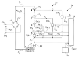
- FIG. 3 shows an electric diagram of an embodiment of an optoelectronic circuit 20 comprising a light-emitting diode switching device and illustrating the general operating principle of the optoelectronic circuit.
- the elements of optoelectronic circuit 20 common with optoelectronic circuit 10 are designated with the same reference numerals.
- optoelectronic circuit 20 comprises rectifying circuit 12 receiving power supply voltage V IN between terminals IN 1 and IN 2 and supplying rectified voltage V ALIM between nodes A 1 and A 2 .
- circuit 20 may directly receive a rectified voltage, and it is then possible for the rectifying circuit not to be present.
- the potential at node A 2 may correspond to a low reference potential V off , for example, 0 V. having the voltages of optoelectronic circuit 20 referenced thereto. Unless otherwise mentioned, the potentials are referenced in the following description to low reference potential V off .
- a high reference potential, called V on may be supplied from power supply voltage V ALIM .
- Optoelectronic circuit 20 comprises M series-connected assemblies of elementary light-emitting diodes, called general light-emitting diodes D i in the following description, where i is an integer in the range from 1 to N and where N is an integer in the range from 2 to 200.
- Each general light-emitting diode DI to DN comprises at least one elementary light-emitting diode.
- each general light-emitting diode is formed of the series and/or parallel assembly of at least two elementary light-emitting diodes.
- the N general light-emitting diodes D i are series-connected, the cathode of general light-emitting diode D i being coupled to the anode of general light-emitting diode D i+1 , for i varying from 1 to N ⁇ 1.
- the anode of general light-emitting diode D 1 is coupled, preferably connected, to node A 1 .
- General light-emitting diodes D i with i varying from 1 to N, may comprise the same number of elementary light-emitting diodes or different numbers of elementary light-emitting diodes.
- Optoelectronic circuit 20 comprises a current source 22 having a terminal coupled to node As and having its other terminal coupled to a node A 3 .
- Current source 22 may have any structure and may in particular correspond to an impedance, for example, a resistor.
- the cathode of general light-emitting diode D N is coupled, preferably connected, to node A 3 .
- Optoelectronic circuit 20 may comprise a circuit, not shown, which supplies a reference voltage to power the current source, possibly obtained from voltage V ALIM .
- Current source 22 may be continuously controlled by a circuit external to optoelectronic circuit 20 .
- Circuit 20 comprises a device 24 for switching general light-emitting diodes D i , with i varying from 1 to N.
- device 24 comprises:
- control circuit 28 capable of receiving voltages VS OURCE and V REF ;
- each conduction circuit SW i with i varying from 1 to N, being assembled between node A 3 and the cathode of general light-emitting diode D i and being controlled by a signal S i supplied by control circuit 28 .
- Conduction circuit SW i is a circuit having an equivalent electric resistance varying between a maximum value and a minimum value according to signal S i . According to an embodiment, when the equivalent electric resistance of conduction circuit SW i is at the maximum value, conduction circuit SW i is substantially equivalent to an off switch. As a variation, current may flow through circuit SW i even when the equivalent electric resistance of conduction circuit SW i is the highest. For i varying from 1 to N, call I i the current flowing through conduction circuit SW i . In the following description, call G i a node coupled to the conduction circuit and receiving signal S i .
- conduction circuit SW N which protects current source 22 from overvoltages, not to be controlled by control unit 28 and to still be on or to be absent, and for the cathode of general light-emitting diode DN to he connected to node A 3 .
- Optoelectronic circuit 20 may further comprise a circuit, not shown, which supplies a reference voltage for the power supply of switching device 24 , possibly obtained from voltage V ALIM .
- control signal S i of each conduction circuit SW i is a signal which may continuously vary between a first value and a second value, the equivalent electric resistance of conduction circuit SW i decreasing when signal S i varies from the first value to the second value.
- the first and second values of signals S i may not be the same for all conduction circuits SW i .
- conduction circuit SW i is substantially not conductive when signal S i is at the first value.
- each conduction circuit SW i is, for example, made of at least one transistor, particularly an enrichment or depletion metal-oxide gate field-effect transistor or MOS transistor.
- Signal Si then is the potential at the gate of transistor SW i .
- each conduction circuit SW i comprises an N-channel enrichment MOS transistor having its drain connected to the cathode of general light-emitting diode D i , having its source coupled to node A 3 and having its gate coupled to node G i .
- conduction circuit SW i comprises two transistors MOS, for example, with an N channel between the cathode of general light-emitting diode D i and node A 3 , the transistor connected to general light-emitting diode D i being a cascade-assembled high-voltage transistor and the transistor connected to node A 3 being a low-voltage transistor controlled by signal S i .
- each conduction circuit may correspond to a transistor other than a MOS transistor, to a relay, to a microelectromechanical system, and generally to any element having an electric conductivity capable of being monotonously voltage- or current-controlled.
- circuit 26 for supplying reference voltage V REF is internal to optoelectronic circuit 20 .
- reference voltage V REF is supplied to optoelectronic circuit 20 by a circuit external to optoelectronic circuit 20 or is obtained from a modulation signal supplied to optoelectronic circuit 20 by a circuit external to optoelectronic circuit 20 .
- optoelectronic circuit 20 may comprise a terminal dedicated to the reception of reference voltage V REF or of the modulation signal from which reference voltage V REF is obtained.
- reference voltage V REF or the modulation signal may be supplied by a dimmer, particularly a dimmer capable of being actuated by a user or a luminosity sensor.
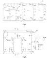
- FIG. 4 shows an electric diagram of an embodiment of control circuit 28 .
- Control circuit 28 comprises a transconductance operational amplifier comprising a differential pair 30 and current mirrors 32 , 34 , and 36 .
- signal S i corresponds to the potential at node G i .
- Differential pair 30 comprises a transistor T 1 , for example, a P-channel MOS transistor having its source coupled to a terminal of a current source I diff and having its gate controlled by voltage V SOURCE .
- the other terminal of current source I diff may be coupled to the source of high reference potential V on .
- Differential pair 30 further comprises a transistor T 2 , for example, a P-channel MOS transistor having its source coupled to current source I diff and having its gate controlled by voltage V REF .
- I 1 the current at the drain of transistor T 1 and I 2 the current at the drain of transistor T 2 .
- transistors T 1 and T 2 have the same characteristics.
- the form factor (W/L) of the channel of transistor T 1 is equal to the form factor of the channel of transistor T 2 .
- the form factor of the channel of a transistor designates the ratio of the width to the length of the channel.
- the form factor of the channel of transistor T 3 is taken as the reference form factor.
- Current mirror 32 comprises a transistor T 3 , for example, an N-channel MOS transistor, having its drain coupled, preferably connected, to the drain of transistor T 1 , having its source coupled, preferably connected, to the source of low reference potential V off , for example, node A 2 , and having its gate coupled to the drain.
- Current mirror 32 comprises a transistor T 4 , for example, an N-channel MOS transistor, having its source coupled, preferably connected, to the source of low reference potential source V off and having its gate coupled to the gate of transistor T 3 .
- transistors T 3 and T 4 have the same characteristics.
- the form factor of the channel of transistor T 3 is equal to the form factor of the channel of transistor T 4 .
- the current flowing through transistor T 4 is thus equal to I 1 flowing through T 3 .
- Current mirror 34 comprises a transistor T 5 , for example, a P-channel MOS transistor, having its drain coupled, preferably connected, to the drain of transistor T 4 , having its source coupled, preferably connected, to the source of low reference potential V on , and having its gate coupled to its drain.
- Current mirror 34 further comprises for each conduction circuit SW i , with i varying from 1 to N, a transistor T sup-i , for example, a P-channel MOS transistor, having its source coupled, preferably connected, to high reference potential source V on , having its gate coupled to the gate of transistor T 5 and having its drain coupled, preferably connected, to node G i .
- transistors T sup-i not to have the same characteristics with respect to one another and with respect to transistor T 5 .
- R sup-i the ratio of the form factor of the channel of transistor T sup-i to the form factor of the channel of transistor T 5 .
- R sup-i may be different from R sup-j , i being different from j.
- IG i the current at the drain of transistor T sup-j .
- Current mirror 36 comprises a transistor T 6 , for example, an N-channel MOS transistor, having its drain coupled, preferably connected, to the drain of transistor T 2 , having its source coupled, preferably connected, to the source of low reference potential V off , and having its gate coupled to its drain.
- Current mirror 36 further comprises for each conduction circuit SW i , with i varying from 1 to N, a MOS transistor T inf-i , for example, an N-channel MOS transistor, having its source coupled, preferably connected, to low reference potential source V off , having its gate coupled to the gate of transistor T 6 , and having its drain coupled, preferably connected, to node G i .
- transistors T inf-i not to have the same characteristics with respect to one another and with respect to transistor T 6 .
- R inf-i the ratio of the form factor of the channel of transistor T inf-i to the form factor of the channel of transistor T 6 .
- R inf-i may be different from R inf-j , being different from j.
- IG′ i the current at the drain of transistor T inf-i .
- RatioPN i the ratio of the form factor of the channel of transistor T sup-i to the form factor of the channel of transistor T inf-i , that is, the ratio of R sup-i to R inf-i .
- ratio RatioPN i is greater than ratio RatioPN j for i greater than j.
- ratio RatioPN i may vary from 1/N to N.
- the difference between RatioPN i and RatioPN i+1 is greater than 1/(N ⁇ 1) ⁇ 1/N.
- FIG. 5 shows an electric diagram of a control circuit 40 comprising all the elements of control circuit 28 shown in FIG. 4 , with the difference that a single conduction circuit SW i is present and that the light-emitting diodes are not present.
- ratios R sup-i and R inf-1 are equal to 1.
- current IG i is equal to current I 1 and current IG′ i is equal to current I 2 .
- voltage V SOURCE is equal to voltage V REF
- currents I 1 , I 2 , IG i , and IG′ i are equal to I diff /2
- the potential at node G i is equal to the sum of voltage V SOURCE and of the gate-source voltage of transistor SW i .
- transistor T 1 conducts less than transistor T 2 , so that current I 1 becomes lower than current I 2 .
- Current IG i decreases with respect to current IG′ i .
- Offset voltage OFFSET i is proportional to the difference between currents I 1 and I 2 and inversely proportional to the conductance of the differential pair. Offset voltage OFFSET i thus depends on ratio RatioPN i . For the same reasons as those previously described, a variation of voltage V SOURCE with respect to its value at equilibrium causes a variation of the voltage at the gate of transistor SW i , which tends to take voltage V SOURCE back to its value at equilibrium. Control circuit 40 thus controls voltage VS OURCE with voltage V REF decreased by offset voltage OFFSET i .
- Control circuit 28 supplies signals S i to S N at values capable of modifying the conduction of conduction circuits SW 1 to SW N so that voltage V SOURCE is controlled by reference voltage V REF to within an offset voltage OFFSET, which may vary according to the operating point of the optoelectronic circuit.
- An advantage of switching device 24 is that it has a decreased current consumption.
- control circuit 28 controls voltage V SOURCE with reference voltage V REF to within an offset voltage OFFSET by controlling the gates of transistors SW i .
- differential pair 30 receives as an input the difference between voltage VS OURCE and reference voltage V REF .
- the reference voltage is identical for all output stages, but the offset voltage is different for each output stage.
- Switch SW i ⁇ 1 thus turns off and, simultaneously, switch SW i becomes less and less conductive. The entire current then flows through switch SW i .
- Control unit 28 then controls voltage V SOURCE with voltage V REF decreased by OFFSET i by means of conduction circuit SW i , offset voltage OFFSET i between voltage V SOURCE and voltage V REF being smaller than offset voltage OFFSET i ⁇ 1 .
- each conduction circuit SW i comprises a MOS transistor having its gate receiving signal S i , this means that the voltage at the gate of transistor SW i ⁇ decreases and transistor SW i ⁇ 1 becomes less and less conductive until it reaches its non-conductive state. At equilibrium, the potential at node G i is equal to the sum of voltage V SOURCE and of the gate-source voltage of transistor SW i .
- Control unit 28 then controls voltage V SOURCE with voltage V REF decreased by OFFSET i ⁇ 1 by means of conduction circuit SW i ⁇ 1 , offset voltage OFFSET i ⁇ 1 being higher than offset voltage OFFSET i .
- each conduction circuit SW i comprises a MOS transistor having its gate receiving signal S i , this means that the voltage at the gate of transistor SW i ⁇ 1 increases and that transistor SW i ⁇ 1 becomes more and more conductive and transistor SW i reaches its totally conductive state.
- control circuit 28 comprises no finite state machines and that the order of the control of conduction circuits S Wi is imposed by the differences between ratios RatioPNi.
- the embodiment of the previously-described method of controlling switches SWi does not depend on the number of elementary light-emitting diodes which form each general light-emitting diode Di and thus does not depend on the threshold voltage of each general light-emitting diode.
- diodes D 1 to D i are conductive and that general light-emitting diodes D i+1 to D N are non-conductive, offset voltage OFFSET i decreasing with index i, the voltage at which voltage V SOURCE stabilizes increases with index i.
- current I SOURCE flowing through general light-emitting diodes D 1 to D i increases with index i.
- a staged increase of current I SOURCE with voltage V ALIM is thus obtained.
- the power factor of the optoelectronic circuit is thus increased.
- circuit 26 for sup-plying reference voltage V REF is capable of modifying the value of reference voltage V REF among a plurality of values according to a control signal supplied by control unit 28 .
- circuit 26 is controlled to increase the value of reference voltage V REF with index i.
- the voltage at which voltage V SOURCE stabilizes then increases with index i, independently from the previously-described increase due to the variation of offset voltage OFFSET i .
- current I SOURCE flowing through general light-emitting diodes D 1 to D i increases with index i.
- a staged increase of current I SOURCE with voltage V ALIM is thus obtained.
- the power factor of the optoelectronic circuit is thus increased.
- current source 22 is capable of supplying a current I SOURCE having an intensity which may take a plurality of values according to a control signal supplied by control unit 28 .
- current source 22 is controlled to increase current intensity I SOURCE with index i.
- the power factor of the optoelectronic circuit is thus increased.
- Offset voltage OFFSET i tor a given i may foe constant or vary according to temperature, either by increasing when the temperature increases, or by decreasing when the temperature increases.
- current source 22 is a resistor and offset voltage OFFSET i decreases when the temperature increases, a temperature increase results in a decrease of current I SOURCE and thus in a decrease of the thermal power supplied by optoelectronic circuit 20 . A protection of optoelectronic circuit 20 against a thermal runaway is thus obtained.
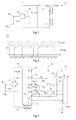
- FIG. 6 shows timing diagrams, obtained by simulation, of voltage V ALIM , of current I SOURCE , of voltages V SOURCE and V REF , of voltages S 1 , S 2 , S 3 , and S 4 and of currents I 1 , I 2 , I 3 , and I 4 in the case where voltage V ALIM is obtained from a sinusoidal voltage V IN and in the case where N is equal to 4.
- ratio RatioPN 1 was equal to 1/4
- ratio RatioPN 2 was equal to 1/3
- ratio RatioPN 3 was equal to 1/2
- RatioPN 4 was equal to 1
- the intensity of the current supplied by current source I diff was equal to 20 ⁇ A.
- each conduction circuit SW i corresponds to a non-conductive state
- these embodiments may also be implemented with a conduction circuit SW i for which the least electrically conductive state however corresponds to a state where current flows through circuit SW i , for example, a current having an intensity smaller than or equal to the theoretical limit, which is the maximum intensity inducing power in conduction circuit SW i capable of being dissipated without causing a malfunction thereof.
- each transistor T sup-i is capable of copying current I 1 multiplied by copying factor R supi and each transistor T inf-i is capable of copying current I 2 multiplied by copying factor R infi .
- each transistor T inf-i may be capable of copying a reference current, for example, a constant current
- each transistor T sup-i is capable of copying current I 1 multiplied by copying factor R supi
- each transistor I sup-i may be capable of copying a reference current, for example, a constant current
- each transistor T inf-i is capable of copying current I 2 multiplied by copying factor R infi .
- Different ratios RatioPN i for each conduction circuit SW i and different offset voltages OFFSET i for conduction circuit SW i may thus also be obtained.
Landscapes
- Led Devices (AREA)
- Amplifiers (AREA)
Abstract
Description
- The present description relates to an optoelectronic circuit, particularly to an optoelectronic circuit comprising light-emitting diodes.
- It is desirable to be able to power an optoelectronic circuit comprising light-emitting diodes with an AC voltage, particularly a sinusoidal voltage, for example, the mains voltage.
-
FIG. 1 shows an example of anoptoelectronic circuit 10 comprising input terminals IN1 and IN2 having an AC voltage VIN applied between them.Optoelectronic circuit 10 further comprises a rectifyingcircuit 12 comprising adiode bridge 14, receiving voltage VIN and supplying a rectified voltage VALIM which powers light-emitting diodes 16, for example, series-assembled with aresistor 15. The current flowing through light-emittingdiodes 16 is called IALIM. -
FIG. 2 is a timing diagram of power supply voltage VALIM and of power supply current IALIM for an example where AC voltage VIN corresponds to a sinusoidal voltage. When voltage VALIM is greater than the sum of the threshold voltages of light-emitting diodes 16, light-emitting diodes 16 become conductive. Power supply current IALIM then follows power supply voltage VALIM. There is therefore an alternation of phases OFF without light emission and of light-emission phases ON. - A disadvantage is that as long as voltage VALIM is smaller than the sum of the threshold voltages of light-
emitting diodes 16, no light is emitted byoptoelectronic circuit 10. An observer may perceive this lack of light emission when the duration of each phase OFF with no light emission between two light-emission phases ON is too long. A possibility, to increase the duration of each phase ON, is to decrease the number of light-emittingdiodes 16. A disadvantage then is that the proportion of electric power lost in the resistor is significant. - Publication US 2014/0252968 describes an optoelectronic circuit where the number of light-emitting diodes receiving power supply voltage VALIM progressively increases during a rising phase of the power supply voltage and progressively decreases during a felling phase of the power supply voltage This is achieved by a switching device capable of short-circuiting a variable number of groups of light-emitting diodes according to the variation of voltage VALIM. This enables to decrease the duration of each phase with no light emission.
- A disadvantage of the optoelectronic circuit described in publication US 2014/0252968 is that it requires using a difference amplifier for each group of light-emitting diodes. The circuit may thus have a high manufacturing cost. Another disadvantage is that the electric power consumption of the optoelectronic circuit may be significant. Another disadvantage is the complexity of the optoelectronic circuit, which may cause reliability issues.
- Publication US-A-2013/0200802 describes an optoelectronic circuit comprising a plurality of series-assembled diodes and a switching device capable of short-circuiting a greater or lesser number of light emitting diodes according to the variation of the power supply voltage. The switching circuit comprises a differential amplifier.
- An object of an embodiment is to overcome all or part of the disadvantages of the previously-described optoelectronic circuits.
- Another object of an embodiment is to decrease the duration of phases -with BO light emission of the optoelectronic circuit.
- Another object of aft embodiment is for the current powering the light-emitting diodes to vary substantially continuously.
- Another object of an embodiment is to have a decreased number of components of the optoelectronic circuit switching device.
- Thus, an embodiment provides an optoelectronic circuit intended to receive a variable voltage containing an alternation of rising and falling phases, the optoelectronic circuit comprising:
-
- assemblies of series-assembled light-emitting diodes;
- a node coupled to each assembly by a conduction circuit having an electric conductance which varies according to a control signal; and
- a control circuit coupled to each conduction circuit comprising a difference amplifier and as many output stages as there are conduction circuits, and capable of supplying each control signal based on the comparison of a first voltage at said node with at least a second voltage identical for all conduction circuits, the control circuit being capable of controlling the first voltage with the second voltage offset by a third voltage, different for each output stage.
- According to an embodiment, the difference amplifier receives as an input a differential voltage corresponding to the difference between the first voltage and the second voltage.
- According to an embodiment, the difference amplifier is capable of supplying a first current and a second current, the control circuit comprising a first current mirror with a plurality of outputs capable of copying, for each conduction circuit, the first current or a third current multiplied by a first copying factor, and a second current mirror with a plurality of outputs capable of copying, for each conduction circuit, the second current or the third current multiplied by a second copying factor, the ratio of the first copying factor to the second copying factor being different for each conduction circuit.
- According to an embodiment, the assemblies of light-emitting diodes are ordered by increasing rank from a first assembly at a first end of the series to a last assembly at a second end of the series and, for each conduction circuit, the control circuit is capable of controlling the first voltage with the second voltage decreased by a third voltage which decreases with the rank of the assembly having the conduction circuit coupled thereto.
- According to an embodiment, the difference amplifier comprises a differential pair comprising a first transistor receiving the first voltage and a second transistor receiving the second voltage.
- According to an embodiment, the first transistor is a MOS transistor having its gate receiving the first voltage and the second transistor is a MOS transistor having its gate receiving the second voltage.
- According to an embodiment, the optoelectronic circuit comprises, for each conduction circuit, a capacitor coupled to the conduction circuit or integrated to the conduction circuit, the first current mirror comprising a capacitor charge circuit and the second current mirror comprising a capacitor discharge circuit.
- According to an embodiment, each conduction circuit comprises a MOS transistor.
- According to an embodiment, the first current mirror comprises, for each conduction circuit, a first copying block coupled to the gate of the MOS transistor of the conduction circuit and capable of supplying the first current multiplied by the first copying factor and the second current mirror comprises, for each conduction circuit, a second copying block coupled to the gate of the MOS transistor of the conduction circuit and capable of supplying the second current multiplied by the second copying factor.
- According to an embodiment, the optoelectronic circuit comprises a current source coupled to said node.
- According to an embodiment, the current source comprises at least one resistor.
- According to an embodiment, the current source is capable of supplying a current which increases with the rank of the assembly having the conduction circuit coupled thereto.
- According to an embodiment, the third voltage varies according to temperature.
- The foregoing and other features and advantages will be discussed in detail in the following non-limiting description of specific embodiments in connection with the accompanying drawings.
-
FIG. 1 , previously described, is an electric diagram of an example of an optoelectronic circuit comprising light-emitting diodes; -
FIG. 2 , previously described, is a timing diagram of the power supply voltage and current of the Sight-emitting diodes of the optoelectronic circuit ofFIG. 1 ; -
FIG. 3 shows an electric diagram of an embodiment of an optoelectronic circuit comprising light-emitting diodes; -
FIG. 4 shows a more detailed electric diagram of an embodiment of the control circuit of the optoelectronic circuit shown inFIG. 3 ; -
FIG. 5 shows a simplified electric diagram illustrating the operation of the control circuit shown inFIG. 4 ; and -
FIG. 6 shows timing diagrams of voltages and of currents during the operation of an embodiment of the optoelectronic circuit ofFIG. 3 . - For clarity, the same elements have been designated with the same reference numerals in the various drawings and, further, the various drawings are not to scale. Unless otherwise specified, expressions “approximately”, “substantially”, and “in the order of” mean to within 10%, preferably to within 5%. Further, a signal which alternates between a first constant state, for example, a low state, noted “0”, and a second constant state, for example, a high state, noted “1”, is called “binary signal”. The high and low states of different binary signals of a same electronic circuit may be different. In particular, the binary signals may correspond to voltages or to currents which may not be perfectly constant in the high or low state. Further, in the present description, term “connected” is used to designate a direct electric connection, with no intermediate electronic component, for example, by means of a conductive track, and term “coupled” or term “linked” will be used to designate either a direct electric -connection (then meaning “connected”) or a connection via one or a plurality of intermediate components (resistor, capacitor, etc.). In the following description, the ratio of the active power consumed by the electronic circuit to the product of the effective values of the current and of the voltage powering the electronic circuit Is called “power factor”.
-
FIG. 3 shows an electric diagram of an embodiment of anoptoelectronic circuit 20 comprising a light-emitting diode switching device and illustrating the general operating principle of the optoelectronic circuit. The elements ofoptoelectronic circuit 20 common withoptoelectronic circuit 10 are designated with the same reference numerals. In particular,optoelectronic circuit 20 comprises rectifyingcircuit 12 receiving power supply voltage VIN between terminals IN1 and IN2 and supplying rectified voltage VALIM between nodes A1 and A2. As a variation,circuit 20 may directly receive a rectified voltage, and it is then possible for the rectifying circuit not to be present. The potential at node A2 may correspond to a low reference potential Voff, for example, 0 V. having the voltages ofoptoelectronic circuit 20 referenced thereto. Unless otherwise mentioned, the potentials are referenced in the following description to low reference potential Voff. A high reference potential, called Von, may be supplied from power supply voltage VALIM. -
Optoelectronic circuit 20 comprises M series-connected assemblies of elementary light-emitting diodes, called general light-emitting diodes Di in the following description, where i is an integer in the range from 1 to N and where N is an integer in the range from 2 to 200. Each general light-emitting diode DI to DN comprises at least one elementary light-emitting diode. Preferably, each general light-emitting diode is formed of the series and/or parallel assembly of at least two elementary light-emitting diodes. In the present example, the N general light-emitting diodes Di are series-connected, the cathode of general light-emitting diode Di being coupled to the anode of general light-emitting diode Di+1, for i varying from 1 toN− 1. The anode of general light-emitting diode D1 is coupled, preferably connected, to node A1. General light-emitting diodes Di, with i varying from 1 to N, may comprise the same number of elementary light-emitting diodes or different numbers of elementary light-emitting diodes. -
Optoelectronic circuit 20 comprises acurrent source 22 having a terminal coupled to node As and having its other terminal coupled to a node A3.Current source 22 may have any structure and may in particular correspond to an impedance, for example, a resistor. The cathode of general light-emitting diode DN is coupled, preferably connected, to node A3. Call VSOURCE the voltage acrosscurrent source 22 and ISOURCE the current flowing throughcurrent source 22.Optoelectronic circuit 20 may comprise a circuit, not shown, which supplies a reference voltage to power the current source, possibly obtained from voltage VALIM.Current source 22 may be continuously controlled by a circuit external tooptoelectronic circuit 20. -
Circuit 20 comprises adevice 24 for switching general light-emitting diodes Di, with i varying from 1 to N. According to an embodiment,device 24 comprises: - a
circuit 26 for supplying a reference voltage VREF; - a
control circuit 28 capable of receiving voltages VSOURCE and VREF; and - N conduction circuits SW1 to SWN, each conduction circuit SWi, with i varying from 1 to N, being assembled between node A3 and the cathode of general light-emitting diode Di and being controlled by a signal Si supplied by
control circuit 28. - Conduction circuit SWi is a circuit having an equivalent electric resistance varying between a maximum value and a minimum value according to signal Si. According to an embodiment, when the equivalent electric resistance of conduction circuit SWi is at the maximum value, conduction circuit SWi is substantially equivalent to an off switch. As a variation, current may flow through circuit SWi even when the equivalent electric resistance of conduction circuit SWi is the highest. For i varying from 1 to N, call Ii the current flowing through conduction circuit SWi. In the following description, call Gi a node coupled to the conduction circuit and receiving signal Si. As a variation, it is possible for conduction circuit SWN, which protects
current source 22 from overvoltages, not to be controlled bycontrol unit 28 and to still be on or to be absent, and for the cathode of general light-emitting diode DN to he connected to node A3. Optoelectronic circuit 20 may further comprise a circuit, not shown, which supplies a reference voltage for the power supply of switchingdevice 24, possibly obtained from voltage VALIM. - In the present embodiment, the control signal Si of each conduction circuit SWi is a signal which may continuously vary between a first value and a second value, the equivalent electric resistance of conduction circuit SWi decreasing when signal Si varies from the first value to the second value. The first and second values of signals Si, with i varying from 1 to N, may not be the same for all conduction circuits SWi. Preferably, conduction circuit SWi is substantially not conductive when signal Si is at the first value.
- According to an embodiment each conduction circuit SWi is, for example, made of at least one transistor, particularly an enrichment or depletion metal-oxide gate field-effect transistor or MOS transistor. Signal Si then is the potential at the gate of transistor SWi. According to an embodiment, each conduction circuit SWi comprises an N-channel enrichment MOS transistor having its drain connected to the cathode of general light-emitting diode Di, having its source coupled to node A3 and having its gate coupled to node Gi. According to another embodiment, conduction circuit SWi comprises two transistors MOS, for example, with an N channel between the cathode of general light-emitting diode Di and node A3, the transistor connected to general light-emitting diode Di being a cascade-assembled high-voltage transistor and the transistor connected to node A3 being a low-voltage transistor controlled by signal Si. This advantageously enables to increase the switching speed of conduction circuit SWi. As a variation, each conduction circuit may correspond to a transistor other than a MOS transistor, to a relay, to a microelectromechanical system, and generally to any element having an electric conductivity capable of being monotonously voltage- or current-controlled.
- According to an embodiment,
circuit 26 for supplying reference voltage VREF is internal tooptoelectronic circuit 20. As a variation, reference voltage VREF is supplied tooptoelectronic circuit 20 by a circuit external tooptoelectronic circuit 20 or is obtained from a modulation signal supplied tooptoelectronic circuit 20 by a circuit external tooptoelectronic circuit 20. As an example,optoelectronic circuit 20 may comprise a terminal dedicated to the reception of reference voltage VREF or of the modulation signal from which reference voltage VREF is obtained. According to an embodiment, reference voltage VREF or the modulation signal may be supplied by a dimmer, particularly a dimmer capable of being actuated by a user or a luminosity sensor. -
FIG. 4 shows an electric diagram of an embodiment ofcontrol circuit 28.Control circuit 28 comprises a transconductance operational amplifier comprising a differential pair 30 andcurrent mirrors 32, 34, and 36. In the present embodiment, signal Si corresponds to the potential at node Gi. - Differential pair 30 comprises a transistor T1, for example, a P-channel MOS transistor having its source coupled to a terminal of a current source Idiff and having its gate controlled by voltage VSOURCE. The other terminal of current source Idiff may be coupled to the source of high reference potential Von. Differential pair 30 further comprises a transistor T2, for example, a P-channel MOS transistor having its source coupled to current source Idiff and having its gate controlled by voltage VREF. Call I1 the current at the drain of transistor T1 and I2 the current at the drain of transistor T2. According to an embodiment, transistors T1 and T2 have the same characteristics. In particular, the form factor (W/L) of the channel of transistor T1 is equal to the form factor of the channel of transistor T2. The form factor of the channel of a transistor designates the ratio of the width to the length of the channel. In the following description, the form factor of the channel of transistor T3 is taken as the reference form factor.
- Current mirror 32 comprises a transistor T3, for example, an N-channel MOS transistor, having its drain coupled, preferably connected, to the drain of transistor T1, having its source coupled, preferably connected, to the source of low reference potential Voff, for example, node A2, and having its gate coupled to the drain. Current mirror 32 comprises a transistor T4, for example, an N-channel MOS transistor, having its source coupled, preferably connected, to the source of low reference potential source Voff and having its gate coupled to the gate of transistor T3. According to an embodiment, transistors T3 and T4 have the same characteristics. In particular, the form factor of the channel of transistor T3 is equal to the form factor of the channel of transistor T4. The current flowing through transistor T4 is thus equal to I1 flowing through T3.
- Current mirror 34 comprises a transistor T5, for example, a P-channel MOS transistor, having its drain coupled, preferably connected, to the drain of transistor T4, having its source coupled, preferably connected, to the source of low reference potential Von, and having its gate coupled to its drain. Current mirror 34 further comprises for each conduction circuit SWi, with i varying from 1 to N, a transistor Tsup-i, for example, a P-channel MOS transistor, having its source coupled, preferably connected, to high reference potential source Von, having its gate coupled to the gate of transistor T5 and having its drain coupled, preferably connected, to node Gi. According to an embodiment, it is possible for transistors Tsup-i not to have the same characteristics with respect to one another and with respect to transistor T5. Call Rsup-i the ratio of the form factor of the channel of transistor Tsup-i to the form factor of the channel of transistor T5. In particular, Rsup-i may be different from Rsup-j, i being different from j. Call IGi the current at the drain of transistor Tsup-j.
-
Current mirror 36 comprises a transistor T6, for example, an N-channel MOS transistor, having its drain coupled, preferably connected, to the drain of transistor T2, having its source coupled, preferably connected, to the source of low reference potential Voff, and having its gate coupled to its drain.Current mirror 36 further comprises for each conduction circuit SWi, with i varying from 1 to N, a MOS transistor Tinf-i, for example, an N-channel MOS transistor, having its source coupled, preferably connected, to low reference potential source Voff, having its gate coupled to the gate of transistor T6, and having its drain coupled, preferably connected, to node Gi. According to an embodiment, it is possible for transistors Tinf-i not to have the same characteristics with respect to one another and with respect to transistor T6. Call Rinf-i the ratio of the form factor of the channel of transistor Tinf-i to the form factor of the channel of transistor T6. In particular, Rinf-i may be different from Rinf-j, being different from j. Call IG′i the current at the drain of transistor Tinf-i. - For i varying from 1 to N, call RatioPNi the ratio of the form factor of the channel of transistor Tsup-i to the form factor of the channel of transistor Tinf-i, that is, the ratio of Rsup-i to Rinf-i. According to an embodiment, ratio RatioPNi is greater than ratio RatioPNj for i greater than j. According to an embodiment, for i varying from 1 to N, ratio RatioPNi may vary from 1/N to N. According to an embodiment, the difference between RatioPNi and RatioPNi+1 is greater than 1/(N−1)−1/N.
- To explain the operation of
optoelectronic circuit 20, a control circuit having a simplified structure will first be considered. -
FIG. 5 shows an electric diagram of acontrol circuit 40 comprising all the elements ofcontrol circuit 28 shown inFIG. 4 , with the difference that a single conduction circuit SWi is present and that the light-emitting diodes are not present. - First consider that ratios Rsup-i and Rinf-1 are equal to 1. In this case, current IGi is equal to current I1 and current IG′i is equal to current I2. At equilibrium, voltage VSOURCE is equal to voltage VREF, currents I1, I2, IGi, and IG′i are equal to Idiff/2, and the potential at node Gi is equal to the sum of voltage VSOURCE and of the gate-source voltage of transistor SWi. When voltage VSOURCE becomes greater than voltage VREF, transistor T1 conducts less than transistor T2, so that current I1 becomes lower than current I2. Current IGi decreases with respect to current IG′i. Due to the capacitance of node Gi, this causes a decrease in the voltage at the gate of transistor SWi. Transistor SWi thus becomes less conductive and voltage VSOURCE decreases until it is equal to VREF again. When voltage VSOURCE becomes lower than voltage VREF, transistor T1 conducts more than transistor T2, so that current I1 becomes greater than current I2. Current IGi increases with respect to current IG′i. Due to the capacitance of node Gi, this causes an increase in the voltage at the gate of transistor SWi. Transistor SWi thus becomes more conductive and voltage VSOURCE rises until it is equal to VREF again.
Control circuit 40 thus controls voltage VSOURCE with voltage VREF. - Now consider that the ratio of Rsup-i to Rinf-i is not equal to 1. The previous line of reasoning remains valid with the difference that, at equilibrium, current I1 is equal to Rinf i*Idiff/(Rinf-1+Rsup-i), current I2 is equal to Rsup-i*Idiff/(Rinf-i+Rsup-i), currents IGi and IG′i are equal to Rinf-i*Rsup-i*Idiff(Rinf-i+Rsup-i), and there is an offset voltage OFFSETi between voltage VSOURCE and voltage VREF. Offset voltage OFFSETi is proportional to the difference between currents I1 and I2 and inversely proportional to the conductance of the differential pair. Offset voltage OFFSETi thus depends on ratio RatioPNi. For the same reasons as those previously described, a variation of voltage VSOURCE with respect to its value at equilibrium causes a variation of the voltage at the gate of transistor SWi, which tends to take voltage VSOURCE back to its value at equilibrium.
Control circuit 40 thus controls voltage VSOURCE with voltage VREF decreased by offset voltage OFFSETi. - Now consider again
optoelectronic circuit 20 shown inFIG. 4 .Control circuit 28 supplies signals Si to SN at values capable of modifying the conduction of conduction circuits SW1 to SWN so that voltage VSOURCE is controlled by reference voltage VREF to within an offset voltage OFFSET, which may vary according to the operating point of the optoelectronic circuit. An advantage of switchingdevice 24 is that it has a decreased current consumption. According to an embodiment, in the case where each conduction circuit SWi comprises a MOS transistor having its gate receiving signal Si,control circuit 28 controls voltage VSOURCE with reference voltage VREF to within an offset voltage OFFSET by controlling the gates of transistors SWi. In other words, differential pair 30 receives as an input the difference between voltage VSOURCE and reference voltage VREF. The reference voltage is identical for all output stages, but the offset voltage is different for each output stage. - In a rising phase of power supply voltage VALIM, while general light-emitting diodes D1 to Di−1 are conductive, general light-emitting diodes Di to DN are non-conductive, signals S1 to Si−2 are at Voff, signals Si to SN are at Von, and signal Si−1 is at a voltage equal to VREF-OFFSETi−1+VGSi−1 enabling switch SWi−1 alone to impose current ISOURCE in the light-emitting diodes, when the voltage across general light-emitting diode Di becomes greater than the threshold voltage of general light-emitting diode Di, the latter becomes conductive and a current starts flowing through general light-emitting diode Di and switch SWi. This results in a temporary decrease of the total equivalent impedance between nodes A1 and A3, and thus in a temporary increase of voltage VSOURCE. As previously described, the increase of voltage VSOURCE causes a decrease in current I1 running through transistor T1 of differential pair 30. Thereby, the current copied by each transistor Tsup-i decreases for i varying from 1 to N. Given that there exists one equivalent capacitor at each node Gi, with 1 varying from 1 to N, capable of corresponding to a different capacitor or to a stray capacitance of another electronic component, and that RatioPNi−1 associated with transistors Tsup-i−1 and Tinf-i−1 coupled to node Gi−1 is smaller than ratios RatioPNi to RatioPNN, the voltage at node Gi−1 decreases until potential Voff is substantially reached while the voltage at node Gi also decreases down to its point of equilibrium, enabling switch SWi alone to impose voltage VSOURCE at VREF-OFFSETi. Switch SWi−1 thus turns off and, simultaneously, switch SWi becomes less and less conductive. The entire current then flows through switch SWi.
Control unit 28 then controls voltage VSOURCE with voltage VREF decreased by OFFSETi by means of conduction circuit SWi, offset voltage OFFSETi between voltage VSOURCE and voltage VREF being smaller than offset voltage OFFSETi−1. In the case where each conduction circuit SWi comprises a MOS transistor having its gate receiving signal Si, this means that the voltage at the gate of transistor SWi−decreases and transistor SWi−1 becomes less and less conductive until it reaches its non-conductive state. At equilibrium, the potential at node Gi is equal to the sum of voltage VSOURCE and of the gate-source voltage of transistor SWi. - In a falling phase of power supply voltage VALIM, while general light-emitting diodes D1 to Di are conductive, general light-emitting diodes Di+1 to DN are non-conductive, signals S1 to Si−1 are at Voff, signals Si+1 to SN are at Von, and signal Si is at a voltage equal to VREF−OFFSETi+VGSi enabling switch SWi alone to impose current ISOURCE in the light-emitting diodes, when the voltage across general light-emitting diode Di decreases and becomes smaller than the threshold voltage of general light-emitting diode Di, the latter starts becoming non-conductive. This results in a temporary increase of the total equivalent impedance between nodes A1 and A3, and thus in a temporary decrease of voltage VSOURCE. As previously described, the decrease of voltage VSOURCE causes an increase in current I1 running through transistor T1 of differential pair 30. Thereby, the current copied by each transistor Tsup-i increases. Given that there exists an equivalent capacitor at each node Gi, and that ratio RatioPNi of branch i is greater than ratio RatioPN1 to RatioPNi−1, the voltage at node Gi increases until it substantially reaches potential Von while the voltage at node Gi−1 also increases up to its point of equilibrium enabling switch SWi−1 alone to impose voltage VSOURCE at VREF−OFFSETj−1. Switch SWi becomes totally conductive and switch SWi−1 becomes more and more conductive. The entire current then flows through switch SWi−1.
Control unit 28 then controls voltage VSOURCE with voltage VREF decreased by OFFSETi−1 by means of conduction circuit SWi−1, offset voltage OFFSETi−1 being higher than offset voltage OFFSETi. In the case where each conduction circuit SWi comprises a MOS transistor having its gate receiving signal Si, this means that the voltage at the gate of transistor SWi−1 increases and that transistor SWi−1 becomes more and more conductive and transistor SWi reaches its totally conductive state. - An advantage of the present embodiment is that
control circuit 28 comprises no finite state machines and that the order of the control of conduction circuits S Wi is imposed by the differences between ratios RatioPNi. - Advantageously, the embodiment of the previously-described method of controlling switches SWi does not depend on the number of elementary light-emitting diodes which form each general light-emitting diode Di and thus does not depend on the threshold voltage of each general light-emitting diode.
- Considering that diodes D1 to Di are conductive and that general light-emitting diodes Di+1 to DN are non-conductive, offset voltage OFFSETi decreasing with index i, the voltage at which voltage VSOURCE stabilizes increases with index i. Thereby, current ISOURCE flowing through general light-emitting diodes D1 to Di increases with index i. A staged increase of current ISOURCE with voltage VALIM is thus obtained. Advantageously, the power factor of the optoelectronic circuit is thus increased.
- According to another embodiment,
circuit 26 for sup-plying reference voltage VREF is capable of modifying the value of reference voltage VREF among a plurality of values according to a control signal supplied bycontrol unit 28. According to an embodiment, considering that diodes D1 to Di are conductive and that general light-emitting diodes Di+1 to DN are non-conductive,circuit 26 is controlled to increase the value of reference voltage VREF with index i. The voltage at which voltage VSOURCE stabilizes then increases with index i, independently from the previously-described increase due to the variation of offset voltage OFFSETi. Thereby, current ISOURCE flowing through general light-emitting diodes D1 to Di increases with index i. A staged increase of current ISOURCE with voltage VALIM is thus obtained. Advantageously, the power factor of the optoelectronic circuit is thus increased. - According to another embodiment,
current source 22 is capable of supplying a current ISOURCE having an intensity which may take a plurality of values according to a control signal supplied bycontrol unit 28. According to an embodiment, considering that diodes D1 to Di are conductive and that general light-emitting diodes Di+1 to DN are non-conductive,current source 22 is controlled to increase current intensity ISOURCE with index i. Advantageously, the power factor of the optoelectronic circuit is thus increased. - Offset voltage OFFSETi tor a given i may foe constant or vary according to temperature, either by increasing when the temperature increases, or by decreasing when the temperature increases. In the case where
current source 22 is a resistor and offset voltage OFFSETi decreases when the temperature increases, a temperature increase results in a decrease of current ISOURCE and thus in a decrease of the thermal power supplied byoptoelectronic circuit 20. A protection ofoptoelectronic circuit 20 against a thermal runaway is thus obtained. -
FIG. 6 shows timing diagrams, obtained by simulation, of voltage VALIM, of current ISOURCE, of voltages VSOURCE and VREF, of voltages S1, S2, S3, and S4 and of currents I1, I2, I3, and I4 in the case where voltage VALIM is obtained from a sinusoidal voltage VIN and in the case where N is equal to 4. To obtain the curves shown inFIG. 6 , ratio RatioPN1 was equal to 1/4, ratio RatioPN2 was equal to 1/3, ratio RatioPN3 was equal to 1/2, and RatioPN4 was equal to 1, and the intensity of the current supplied by current source Idiff was equal to 20 μA. - Specific embodiments have been described. Various alterations, modifications, and improvements will readily occur to those skilled in the art. Although detailed embodiments have been described, where the least electrically conductive conduction state of each conduction circuit SWi corresponds to a non-conductive state, it should be clear that these embodiments may also be implemented with a conduction circuit SWi for which the least electrically conductive state however corresponds to a state where current flows through circuit SWi, for example, a current having an intensity smaller than or equal to the theoretical limit, which is the maximum intensity inducing power in conduction circuit SWi capable of being dissipated without causing a malfunction thereof.
- Further, in the previously-described embodiments, each transistor Tsup-i is capable of copying current I1 multiplied by copying factor Rsupi and each transistor Tinf-i is capable of copying current I2 multiplied by copying factor Rinfi. As a variation, each transistor Tinf-i may be capable of copying a reference current, for example, a constant current, and each transistor Tsup-i is capable of copying current I1 multiplied by copying factor Rsupi. As a variation, each transistor Isup-i may be capable of copying a reference current, for example, a constant current, and each transistor Tinf-i is capable of copying current I2 multiplied by copying factor Rinfi. Different ratios RatioPNi for each conduction circuit SWi and different offset voltages OFFSETi for conduction circuit SWi may thus also be obtained.
- Such alterations, modifications, and improvements are intended to be part of this disclosure, and are intended to be within the spirit and the scope of the present invention. Accordingly, the foregoing description is by way of example only and is not intended to be limiting. The present invention is limited only as defined in the following claims and the equivalents thereto.
Claims (13)
Applications Claiming Priority (2)
| Application Number | Priority Date | Filing Date | Title |
|---|---|---|---|
| FR1659452A FR3057135B1 (en) | 2016-09-30 | 2016-09-30 | OPTOELECTRONIC CIRCUIT INCLUDING LIGHT-LUMINESCENT DIODES |
| FR1659452 | 2016-09-30 |
Publications (2)
| Publication Number | Publication Date |
|---|---|
| US20180098394A1 true US20180098394A1 (en) | 2018-04-05 |
| US9974133B2 US9974133B2 (en) | 2018-05-15 |
Family
ID=57750154
Family Applications (1)
| Application Number | Title | Priority Date | Filing Date |
|---|---|---|---|
| US15/719,612 Active US9974133B2 (en) | 2016-09-30 | 2017-09-29 | Optoelectronic circuit comprising light-emitting diodes |
Country Status (3)
| Country | Link |
|---|---|
| US (1) | US9974133B2 (en) |
| EP (1) | EP3302003B1 (en) |
| FR (1) | FR3057135B1 (en) |
Families Citing this family (1)
| Publication number | Priority date | Publication date | Assignee | Title |
|---|---|---|---|---|
| FR3144481A1 (en) * | 2022-12-26 | 2024-06-28 | Easii Ic | OPTOELECTRONIC CIRCUIT INCLUDING LIGHT-EMITTING DIODES |
Family Cites Families (2)
| Publication number | Priority date | Publication date | Assignee | Title |
|---|---|---|---|---|
| KR100986815B1 (en) * | 2010-02-05 | 2010-10-13 | 신봉섭 | Constant current driving apparatus for light emitting diode |
| US8680782B2 (en) * | 2012-02-03 | 2014-03-25 | Nichia Corporation | Light-emitting diode driving apparatus |
-
2016
- 2016-09-30 FR FR1659452A patent/FR3057135B1/en active Active
-
2017
- 2017-09-29 EP EP17193974.7A patent/EP3302003B1/en active Active
- 2017-09-29 US US15/719,612 patent/US9974133B2/en active Active
Also Published As
| Publication number | Publication date |
|---|---|
| FR3057135A1 (en) | 2018-04-06 |
| US9974133B2 (en) | 2018-05-15 |
| EP3302003A1 (en) | 2018-04-04 |
| EP3302003B1 (en) | 2019-04-24 |
| FR3057135B1 (en) | 2020-11-13 |
Similar Documents
| Publication | Publication Date | Title |
|---|---|---|
| US9277615B2 (en) | LED drive circuit | |
| US9414453B2 (en) | Lighting device | |
| US9831856B2 (en) | Electronic drive circuit and method | |
| US9559668B2 (en) | Drive circuit and semiconductor apparatus | |
| US8450942B2 (en) | Light emitting diode driving apparatus | |
| US8957724B2 (en) | Low electromagnetic emission driver | |
| US20190158027A1 (en) | High speed, high voltage, amplifier output stage using linear or class D topology | |
| US8476838B2 (en) | Light source lighting circuit and lamp system for vehicle | |
| EP2410820A2 (en) | Semiconductor light source lighting circuit and control method | |
| US7834678B2 (en) | Circuit arrangement and method of driving a circuit arrangement | |
| US7508254B2 (en) | Reference supply voltage circuit using more than two reference supply voltages | |
| US9974133B2 (en) | Optoelectronic circuit comprising light-emitting diodes | |
| KR101400606B1 (en) | LED lighting driving circuit | |
| US11522535B2 (en) | Semiconductor device | |
| TWI544464B (en) | Pixel units and driving circuits | |
| US8907583B1 (en) | LED driving device | |
| US10085319B1 (en) | Lighting apparatus | |
| US8692589B2 (en) | Semiconductor element driving circuit and semiconductor device | |
| RU2487392C2 (en) | Redundant voltage stabiliser based on mis transistors | |
| US10076008B2 (en) | Optoelectronic circuit comprising light-emitting diodes | |
| US9615419B2 (en) | AC LED driving circuit | |
| KR101233354B1 (en) | Semiconductor Switch | |
| US10064250B2 (en) | Optoelectronic circuit comprising light-emitting diodes | |
| KR20230009658A (en) | Apparatus for supplying power to drive Alternating Current (AC) direct-coupled light-emitting diodes (LED) | |
| US20200136610A1 (en) | Floating switch and drive circuit thereof |
Legal Events
| Date | Code | Title | Description |
|---|---|---|---|
| FEPP | Fee payment procedure |
Free format text: ENTITY STATUS SET TO UNDISCOUNTED (ORIGINAL EVENT CODE: BIG.) |
|
| FEPP | Fee payment procedure |
Free format text: ENTITY STATUS SET TO SMALL (ORIGINAL EVENT CODE: SMAL) |
|
| AS | Assignment |
Owner name: EASII IC, FRANCE Free format text: ASSIGNMENT OF ASSIGNORS INTEREST;ASSIGNORS:GRAS, DAVID;PEYSSON, THOMAS;REEL/FRAME:043978/0229 Effective date: 20171006 |
|
| STCF | Information on status: patent grant |
Free format text: PATENTED CASE |
|
| MAFP | Maintenance fee payment |
Free format text: PAYMENT OF MAINTENANCE FEE, 4TH YR, SMALL ENTITY (ORIGINAL EVENT CODE: M2551); ENTITY STATUS OF PATENT OWNER: SMALL ENTITY Year of fee payment: 4 |
|
| FEPP | Fee payment procedure |
Free format text: MAINTENANCE FEE REMINDER MAILED (ORIGINAL EVENT CODE: REM.); ENTITY STATUS OF PATENT OWNER: SMALL ENTITY |