US20180098005A1 - Solid-state imaging device and electronic device - Google Patents
Solid-state imaging device and electronic device Download PDFInfo
- Publication number
- US20180098005A1 US20180098005A1 US15/560,645 US201615560645A US2018098005A1 US 20180098005 A1 US20180098005 A1 US 20180098005A1 US 201615560645 A US201615560645 A US 201615560645A US 2018098005 A1 US2018098005 A1 US 2018098005A1
- Authority
- US
- United States
- Prior art keywords
- voltage
- pixel
- solid
- state imaging
- imaging device
- Prior art date
- Legal status (The legal status is an assumption and is not a legal conclusion. Google has not performed a legal analysis and makes no representation as to the accuracy of the status listed.)
- Granted
Links
Images
Classifications
-
- H04N5/359—
-
- H—ELECTRICITY
- H04—ELECTRIC COMMUNICATION TECHNIQUE
- H04N—PICTORIAL COMMUNICATION, e.g. TELEVISION
- H04N25/00—Circuitry of solid-state image sensors [SSIS]; Control thereof
- H04N25/70—SSIS architectures; Circuits associated therewith
- H04N25/76—Addressed sensors, e.g. MOS or CMOS sensors
- H04N25/77—Pixel circuitry, e.g. memories, A/D converters, pixel amplifiers, shared circuits or shared components
- H04N25/772—Pixel circuitry, e.g. memories, A/D converters, pixel amplifiers, shared circuits or shared components comprising A/D, V/T, V/F, I/T or I/F converters
-
- H—ELECTRICITY
- H04—ELECTRIC COMMUNICATION TECHNIQUE
- H04N—PICTORIAL COMMUNICATION, e.g. TELEVISION
- H04N25/00—Circuitry of solid-state image sensors [SSIS]; Control thereof
- H04N25/60—Noise processing, e.g. detecting, correcting, reducing or removing noise
- H04N25/62—Detection or reduction of noise due to excess charges produced by the exposure, e.g. smear, blooming, ghost image, crosstalk or leakage between pixels
- H04N25/627—Detection or reduction of inverted contrast or eclipsing effects
-
- H—ELECTRICITY
- H04—ELECTRIC COMMUNICATION TECHNIQUE
- H04N—PICTORIAL COMMUNICATION, e.g. TELEVISION
- H04N25/00—Circuitry of solid-state image sensors [SSIS]; Control thereof
- H04N25/70—SSIS architectures; Circuits associated therewith
- H04N25/76—Addressed sensors, e.g. MOS or CMOS sensors
-
- H—ELECTRICITY
- H04—ELECTRIC COMMUNICATION TECHNIQUE
- H04N—PICTORIAL COMMUNICATION, e.g. TELEVISION
- H04N25/00—Circuitry of solid-state image sensors [SSIS]; Control thereof
- H04N25/70—SSIS architectures; Circuits associated therewith
- H04N25/76—Addressed sensors, e.g. MOS or CMOS sensors
- H04N25/77—Pixel circuitry, e.g. memories, A/D converters, pixel amplifiers, shared circuits or shared components
- H04N25/778—Pixel circuitry, e.g. memories, A/D converters, pixel amplifiers, shared circuits or shared components comprising amplifiers shared between a plurality of pixels, i.e. at least one part of the amplifier must be on the sensor array itself
-
- H—ELECTRICITY
- H04—ELECTRIC COMMUNICATION TECHNIQUE
- H04N—PICTORIAL COMMUNICATION, e.g. TELEVISION
- H04N25/00—Circuitry of solid-state image sensors [SSIS]; Control thereof
- H04N25/70—SSIS architectures; Circuits associated therewith
- H04N25/76—Addressed sensors, e.g. MOS or CMOS sensors
- H04N25/78—Readout circuits for addressed sensors, e.g. output amplifiers or A/D converters
-
- H04N5/37455—
-
- H04N5/378—
Definitions
- the present technology relates to a solid-state imaging device and an electronic device, and particularly relates to a solid-state imaging device and an electronic device that enable a reduction in the voltage of an AD conversion circuit.
- a phenomenon occurs in which a portion that originally is to be bright in an image becomes black.
- the black portion in the image is also called a sunspot etc., because it looks like a sunspot.
- the sunspot is caused by fluctuation of a reset level, which occurs when a large amount of charge generated in a photodiode (PD) constituting a pixel leaks to a floating diffusion (FD) or the FD is directly exposed to light.
- PD photodiode
- FD floating diffusion
- Patent Literature 1 describes that a clipping circuit limits the potential of a vertical signal line to different potentials between in reset level reading and in signal level reading.
- Patent Literature 1 JP 2012-85343A
- the gate voltage of the clipping circuit needs to be set to include some margin, in consideration of this variation. Accordingly, also a dynamic range of an AD conversion circuit needs to be set to include a margin similarly. That is, it is necessary to design the AD conversion circuit in consideration of at least a voltage corresponding to this margin, which hinders a reduction in the voltage of the AD conversion circuit.
- the present technology has been made in view of such circumstances, and enables a reduction in the voltage of an AD conversion circuit.
- a solid-state imaging device of an aspect of the present technology includes: a plurality of pixels; a vertical signal line configured to output a pixel signal of the pixel; and a clipping circuit configured to limit a voltage of the vertical signal line to a predetermined voltage.
- the clipping circuit includes a transistor configured to generate the predetermined voltage in accordance with a voltage of a gate, and a sample holding circuit configured to hold a reset level of the pixel that is output to the vertical signal line, and input the reset level to the gate of the transistor.
- the clipping circuit can further include a capacitor having one electrode connected to the gate of the transistor, and a voltage generation circuit configured to generate a plurality of different voltages can be connected to the other electrode of the capacitor.
- the voltage generation circuit can apply different voltages to the capacitor between in reading the reset level of the pixel and in reading a signal level of the pixel.
- the clipping circuit can include a plurality of the capacitors, and the voltage generation circuit can apply a first voltage to one capacitor in reading the reset level of the pixel, and apply a second voltage to another capacitor in reading a signal level of the pixel.
- the clipping circuit can further include a selector configured to turn on/off a limitation on the voltage of the vertical signal line using the predetermined voltage generated by the transistor.
- An electronic device of an aspect of the present technology includes a solid-state imaging device including a plurality of pixels, a vertical signal line configured to output a pixel signal of the pixel, and a clipping circuit configured to limit a voltage of the vertical signal line to a predetermined voltage.
- the clipping circuit includes a transistor configured to generate the predetermined voltage in accordance with a voltage of a gate, and a sample holding circuit configured to hold a reset level of the pixel that is output to the vertical signal line, and input the reset level to the gate of the transistor.
- the predetermined voltage is generated in accordance with the voltage of the gate, and the reset level of the pixel that is output to the vertical signal line is held and input to the gate of the transistor.
- the voltage of an AD conversion circuit can be reduced.
- FIG. 1 is a block diagram illustrating a configuration example of a solid-state imaging device of the present technology.
- FIG. 2 is a diagram for describing a structure of a solid-state imaging device.
- FIG. 3 illustrates a circuit configuration example of a solid-state imaging device of the present technology.
- FIG. 4 is a timing chart illustrating the operation of a solid-state imaging device of the present technology.
- FIG. 5 illustrates a circuit configuration example of a solid-state imaging device of the present technology.
- FIG. 6 is a timing chart illustrating the operation of a solid-state imaging device of the present technology.
- FIG. 7 illustrates a circuit configuration example of a conventional solid-state imaging device.
- FIG. 8 is a timing chart illustrating the operation of a conventional solid-state imaging device.
- FIG. 9 is a timing chart illustrating the operation of a conventional solid-state imaging device.
- FIG. 10 illustrates a circuit configuration example of a solid-state imaging device of a first embodiment.
- FIG. 11 is a timing chart illustrating the operation of the solid-state imaging device of the first embodiment.
- FIG. 12 illustrates a circuit configuration example of a solid-state imaging device of a second embodiment.
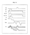
- FIG. 13 is a timing chart illustrating the operation of the solid-state imaging device of the second embodiment.
- FIG. 14 illustrates a circuit configuration example of a solid-state imaging device of a third embodiment.
- FIG. 15 illustrates a circuit configuration example of a solid-state imaging device of a fourth embodiment.
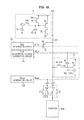
- FIG. 16 illustrates a circuit modification example of a configuration of a solid-state imaging device of the present technology.
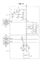
- FIG. 17 illustrates a circuit modification example of a configuration of a solid-state imaging device of the present technology.
- FIG. 18 illustrates a circuit modification example of a configuration of a solid-state imaging device of the present technology.
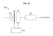
- FIG. 19 is a block diagram illustrating a configuration example of an electronic device of the present technology.
- FIG. 20 illustrates usage examples of an image sensor.
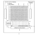
- FIG. 1 is a block diagram illustrating a configuration example of a solid-state imaging device of the present technology.
- a solid-state imaging device 1 is configured as a complementary metal oxide semiconductor (CMOS) image sensor.
- the solid-state imaging device 1 includes a pixel area (pixel array) 3 in which a plurality of pixels 2 are regularly arranged in a two-dimensional array in a semiconductor substrate (e.g., a Si substrate), which is not illustrated, and a peripheral circuit unit.
- CMOS complementary metal oxide semiconductor
- the pixel 2 includes a photoelectric conversion unit (e.g., a photodiode) and a plurality of pixel transistors (MOS transistors).
- the plurality of pixel transistors may include, for example, three transistors of a transfer transistor, a reset transistor, and an amplification transistor.
- the plurality of pixel transistors may include four transistors including a selection transistor in addition to the three transistors.
- the pixel 2 may be configured as one unit pixel, or may be in a pixel sharing structure.
- This pixel sharing structure is a structure in which a plurality of photodiodes share a floating diffusion and transistors other than a transfer transistor.
- the peripheral circuit unit includes a vertical drive circuit 4 , column signal processing circuits 5 , a horizontal drive circuit 6 , an output circuit 7 , and a control circuit 8 .
- the control circuit 8 receives an input clock and data commanding an operation mode or the like, and outputs data such as internal information of the solid-state imaging device 1 .
- the control circuit 8 on the basis of a vertical synchronizing signal, a horizontal synchronizing signal, and a master clock, the control circuit 8 generates a clock signal and a control signal that serve as a reference for the operation of the vertical drive circuit 4 , the column signal processing circuits 5 , the horizontal drive circuit 6 , and the like. Then, the control circuit 8 inputs these signals to the vertical drive circuit 4 , the column signal processing circuits 5 , the horizontal drive circuit 6 , and the like.
- the vertical drive circuit 4 is constituted by a shift register, for example.
- the vertical drive circuit 4 selects a pixel drive line, and supplies a pulse for driving pixels to the selected pixel drive line to drive pixels in units of rows. That is, the vertical drive circuit 4 selectively scans the pixels 2 of the pixel area 3 sequentially in the vertical direction in units of rows. Then, the vertical drive circuit 4 supplies pixel signals based on signal charge generated in accordance with the amount of received light in the photoelectric conversion units of the respective pixels 2 to the column signal processing circuits 5 through vertical signal lines 9 .
- the column signal processing circuit 5 is disposed for each column of the pixels 2 , for example.
- the column signal processing circuits 5 perform signal processing such as noise cancellation on signals output from the pixels 2 of one row, in units of pixel columns.
- the column signal processing circuits 5 perform signal processing such as correlated double sampling (CDS) for cancelling fixed pattern noise peculiar to the pixel 2 , signal amplification, and analog-digital (AD) conversion.
- CDS correlated double sampling
- AD analog-digital
- a horizontal selection switch (not illustrated) is provided to be connected to a horizontal signal line 10 .
- the horizontal drive circuit 6 is constituted by a shift register, for example.
- the horizontal drive circuit 6 sequentially outputs a horizontal scanning pulse to select the column signal processing circuits 5 in order, and causes the column signal processing circuits 5 to output pixel signals to the horizontal signal line 10 .
- the output circuit 7 performs signal processing on signals sequentially supplied from the column signal processing circuits 5 through the horizontal signal line 10 , and outputs the resulting signals. For example, the output circuit 7 performs only buffering in some cases, and performs black level adjustment, column variation correction, various digital signal processing, and the like in some cases.
- Input/output terminals 12 exchange signals with the outside.
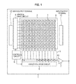
- a solid-state imaging device la illustrated in the upper stage of FIG. 2 includes a semiconductor substrate 20 .
- the semiconductor substrate 20 is equipped with a pixel area 23 , a control circuit 24 , and a logic circuit 25 including a signal processing circuit.
- the solid-state imaging device 1 a is configured as one semiconductor chip.
- a solid-state imaging device 1 b illustrated in the middle stage of FIG. 2 includes a first semiconductor substrate 21 and a second semiconductor substrate 22 .
- the first semiconductor substrate 21 is equipped with the pixel area 23 and the control circuit 24 .
- the second semiconductor substrate 22 is equipped with the logic circuit 25 including a signal processing circuit.
- the first semiconductor substrate 21 and the second semiconductor substrate 22 are electrically connected to each other to constitute the stacked-type solid-state imaging device 1 b serving as one semiconductor chip.
- a solid-state imaging device 1 c illustrated in the lower stage of FIG. 2 includes the first semiconductor substrate 21 and the second semiconductor substrate 22 .
- the first semiconductor substrate 21 is equipped with the pixel area 23 .
- the second semiconductor substrate 22 is equipped with the control circuit 24 and the logic circuit 25 including a signal processing circuit.
- the first semiconductor substrate 21 and the second semiconductor substrate 22 are electrically connected to each other to constitute the stacked-type solid-state imaging device 1 c serving as one semiconductor chip.
- a configuration that electrically connects the first semiconductor substrate 21 and the second semiconductor substrate 22 may be a through via, Cu—Cu metallic bonding, or other configurations.
- the second semiconductor substrate 22 includes one layer in the above description, but may include two or more layers. That is, the present technology is also applicable to a solid-state imaging device made of a stack of three or more layers including the first semiconductor substrate 21 as the uppermost layer.
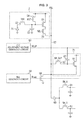
- FIG. 3 illustrates a circuit configuration example of the solid-state imaging device 1 of the present technology.
- the pixel 2 includes a photodiode (PD) 51 serving as a photoelectric conversion unit, a transfer transistor 52 , a floating capacitance 53 , a reset transistor 54 , an amplification transistor 55 , and a selection transistor 56 .
- PD photodiode
- all the pixel transistors included in the pixel 2 are configured as n-channel MOS transistors.
- An anode of the PD 51 is grounded, and a cathode of the PD 51 is connected to a source of the transfer transistor 52 .
- a drain of the transfer transistor 52 is connected to a gate of the amplification transistor 55 , and this connection point constitutes a floating diffusion (FD).
- the reset transistor 54 is connected between a predetermined power source and the FD.
- a drain of the amplification transistor 55 is connected to the predetermined power source, and a source of the amplification transistor 55 is connected to a drain of the selection transistor 56 .
- a source of the selection transistor 56 is connected to a vertical signal line 57 .
- the vertical signal line 57 is connected to a load MOS transistor 58 .
- Bias voltage generated by a Bias generation circuit 59 is supplied to the load MOS transistor 58 .
- the amplification transistor 55 and the load MOS transistor 58 constitute a source follower circuit.
- the voltage of the vertical signal line 57 (a pixel signal) is read from an output terminal 60 .
- the output of the output terminal 60 is held by a sample holding circuit 61 or a sample holding circuit 62 .
- the sample holding circuit 61 holds the voltage (reset level) of the vertical signal line 57 corresponding to the potential of the FD when the FD is reset.
- the sample holding circuit 62 holds the voltage (signal level) of the vertical signal line 57 corresponding to the potential of the FD when charge of the PD 51 is transferred to the FD.
- a clipping circuit 71 is connected to the vertical signal line 57 .
- the clipping circuit 71 limits (clips) the voltage of the vertical signal line 57 to a predetermined voltage.
- the clipping circuit 71 includes a clipping transistor 81 , a sample holding circuit 82 , and a capacitor 83 .
- the clipping transistor 81 generates a voltage to limit the voltage of the vertical signal line 57 , in accordance with a clipping voltage CLP applied to its gate.
- the sample holding circuit 82 holds the voltage of the vertical signal line 57 , and inputs the voltage to the gate of the clipping transistor 81 .
- One electrode of the capacitor 83 is connected to the gate of the clipping transistor 81 .
- the other electrode of the capacitor 83 is connected to a CLP adjustment voltage generation circuit 91 .
- the CLP adjustment voltage generation circuit 91 generates an adjustment voltage VCLP for adjusting the clipping voltage CLP, and applies the adjustment voltage VCLP to the capacitor 83 .
- TRG is a drive signal for driving the transfer transistor 52 .
- RST is a drive signal for driving the reset transistor 54 .
- SEL is a drive signal for driving the selection transistor 56 .
- SH_CLP is a drive signal for driving the sample holding circuit 82 .
- SH_R is a drive signal for driving the sample holding circuit 61 .
- SH_S is a drive signal for driving the sample holding circuit 62 .
- VCLP is an adjustment voltage for adjusting the clipping voltage CLP.
- the sample holding circuit 61 holds the reset level. That is, the reset level of the pixel 2 is read.
- the sample holding circuit 62 holds the voltage (signal level) of the vertical signal line 57 corresponding to the potential of the FD when charge of the PD 51 is transferred to the FD. That is, the signal level of the pixel 2 is read.
- the CLP adjustment voltage generation circuit 91 applies different adjustment voltages VCLP to the capacitor 83 between in reading the reset level of the pixel 2 and in reading the signal level of the pixel 2 .
- the CLP adjustment voltage generation circuit 91 applies an adjustment voltage VCLP_R to the capacitor 83 in reading the reset level of the pixel 2 .
- the clipping voltage CLP applied to the gate of the clipping transistor 81 is adjusted, and the voltage of the vertical signal line 57 is limited to a first voltage.
- the CLP adjustment voltage generation circuit 91 applies an adjustment voltage VCLP_S lower than the adjustment voltage VCLP_R to the capacitor 83 in reading the signal level of the pixel 2 .
- the clipping voltage CLP applied to the gate of the clipping transistor 81 is adjusted, and the voltage of the vertical signal line 57 is limited to a second voltage.
- the adjustment voltage VCLP_R and the adjustment voltage VCLP_S can be variable in accordance with the amount of adjustment of the clipping voltage CLP.
- the high-low relationship between the adjustment voltage VCLP_R and the adjustment voltage VCLP_S is reversed depending on the polarity of transistors included in the pixel 2 .
- FIG. 5 illustrates another circuit configuration example of the solid-state imaging device 1 of the present technology.
- the configuration in FIG. 5 is basically similar to the configuration in FIG. 3 , but differs in that the clipping circuit 71 further includes a selector 111 .
- the selector 111 turns on/off the limitation on the voltage of the vertical signal line 57 using a voltage generated by the transistor 81 .
- drive signals and adjustment voltages are similar to those illustrated in FIG. 4 , except for SEL_CLP.
- SEL_CLP is a drive signal for driving the selector 111 .
- the drive signal SEL_CLP is in the H state in a period from the time of reading the reset level of the pixel 2 to the time of reading the signal level of the pixel 2 .
- the selector 111 turns on the limitation on the voltage of the vertical signal line 57 using a voltage generated by the transistor 81 .
- the operation in this case is similar to the operation described with reference to FIG. 4 .
- the drive signal SEL_CLP is in the H state only in reading the reset level of the pixel 2 .
- the selector 111 turns on the limitation on the voltage of the vertical signal line 57 using a voltage generated by the transistor 81 .
- the selector 111 turns off the limitation on the voltage of the vertical signal line 57 using a voltage generated by the transistor 81 .
- the selector 111 may turn off the limitation on the voltage of the vertical signal line 57 using a voltage generated by the transistor 81 , only in reading the signal level. Furthermore, the limitation on the voltage of the vertical signal line 57 may be turned on/off for each pixel column as necessary.
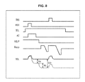
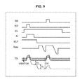
- FIG. 7 illustrates a circuit configuration example of a conventional solid-state imaging device.
- the solid-state imaging device illustrated in FIG. 7 includes a single-slope AD conversion circuit.
- a clipping circuit 121 includes the clipping transistor 81 .
- the clipping transistor 81 generates a voltage to limit the voltage of the vertical signal line 57 , in accordance with an adjustment voltage VCLP applied to its gate.
- a Ramp generation circuit 122 generates a reference signal Ramp that exhibits a ramp waveform having a predetermined slope at a predetermined timing.
- the reference signal Ramp is input to one terminal of a comparator 123 .
- the comparator 123 compares the reference signal Ramp input to one terminal with a pixel signal input to the other terminal.
- the comparator 123 outputs a signal whose level is inverted in accordance with the magnitude relationship between the reference signal Ramp and the pixel signal to a counter 124 .
- the counter 124 executes up-count operation and down-count operation while switching between them.
- the counter 124 ends the up-count operation and the down-count operation in accordance with a timing at which the output of the comparator 123 is inverted.
- Count values obtained by the up-count operation and the down-count operation are output as digital data.
- the two terminals of the comparator 123 are each configured in a manner that offset is cancelled (auto zero) by an AZ switch.
- the comparator 123 and the counter 124 constitute a single-slope AD conversion circuit.
- TRG is a drive signal for driving the transfer transistor 52 .
- RST is a drive signal for driving the reset transistor 54 .
- SEL is a drive signal for driving the selection transistor 56 .
- AZ is a drive signal for driving the AZ switches of the comparator 123 .
- VCLP is an adjustment voltage generated by the CLP adjustment voltage generation circuit 91 .
- Ramp is a reference signal generated by the Ramp generation circuit 122 .
- VSL is the voltage of the vertical signal line 57 , that is, a pixel signal.
- the solid line indicates a pixel signal in a state (dark) where charge of the PD does not leak to the FD.
- the dotted line indicates a pixel signal in a state (light) where charge of the PD leaks to the FD and a sunspot occurs.
- the CLP adjustment voltage generation circuit 91 applies different adjustment voltages VCLP to the gate of the transistor 81 between in reading the reset level of the pixel 2 and in reading the signal level of the pixel 2 . Such operation enables the reset level and the signal level to be clipped appropriately.
- VSL light pixel signal
- a voltage difference Va between the dark pixel signal and the light pixel signal exhibits a voltage difference equal to or more than a voltage difference that does not interfere with a normal pixel. Furthermore, a voltage difference Vb between in reset level reading and in signal level reading of the light pixel signal exhibits a voltage difference by which it can be determined that a sunspot has occurred.
- the gate voltage of the transistor 81 of the clipping circuit 121 needs to be set to include some margin, in consideration of this variation. Accordingly, also the dynamic range Vdr of the AD conversion circuit needs to be set to include a margin similarly. That is, it is necessary to design the AD conversion circuit in consideration of at least a voltage corresponding to this margin.
- a reset level is held and input to the gate of the clipping transistor 81 .
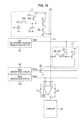
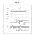
- FIG. 10 illustrates a circuit configuration example of a solid-state imaging device of a first embodiment of the present technology.
- the solid-state imaging device illustrated in FIG. 10 includes a single-slope AD conversion circuit.
- the solid-state imaging device illustrated in FIG. 10 includes, as a clipping circuit, the clipping circuit 71 described with reference to FIG. 3 .
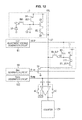
- FIG. 12 illustrates a circuit configuration example of a solid-state imaging device of a second embodiment of the present technology.
- the solid-state imaging device illustrated in FIG. 12 also includes a single-slope AD conversion circuit.
- the solid-state imaging device illustrated in FIG. 12 includes, as a clipping circuit, the clipping circuit 71 described with reference to FIG. 5 .
- the selector 111 may turn off the limitation on the voltage of the vertical signal line 57 using a voltage generated by the transistor 81 , only in reset level reading or only in signal level reading. Furthermore, the limitation on the voltage of the vertical signal line 57 may be turned on/off for each pixel column as necessary.
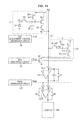
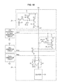
- FIG. 14 illustrates a circuit configuration example of a solid-state imaging device of a third embodiment of the present technology.
- the solid-state imaging device illustrated in FIG. 14 includes, in addition to the configuration in FIG. 12 , a gain amplifier 131 preceding the comparator 123 .
- the gain amplifier 131 amplifies the voltage of the vertical signal line 57 , that is, a pixel signal, and supplies the amplified voltage to the comparator 123 .
- FIG. 15 illustrates a circuit configuration example of a solid-state imaging device of a fourth embodiment of the present technology.
- the solid-state imaging device illustrated in FIG. 15 includes, in place of the capacitor 83 of the clipping circuit 71 in the configuration in FIG. 12 , two capacitors 83 -R and 83 -S.
- One electrode of each of the capacitors 83 -R and 83 -S is connected to the gate of the clipping transistor 81 .
- the other electrode of each capacitor 83 is connected to a CLP adjustment voltage generation circuit 141 .
- the CLP adjustment voltage generation circuit 141 generates an adjustment voltage VCLP_R and applies it to the capacitor 83 -R in reading the reset level of the pixel 2 .
- the CLP adjustment voltage generation circuit 141 generates an adjustment voltage VCLP_S lower than the adjustment voltage VCLP_R and applies it to the capacitor 83 -S in reading the signal level of the pixel 2 .
- a solid-state imaging device of the present technology can have a stacked structure.
- the clipping circuit 71 may be provided not in the first semiconductor substrate 21 including the pixels 2 (the pixel area 23 ) but in the second semiconductor substrate 22 including the logic circuit 25 .
- the clipping circuit 71 may be provided not in the second semiconductor substrate 22 including the logic circuit 25 but in the first semiconductor substrate 21 including the pixels 2 (the pixel area 23 ).
- the clipping circuit may be provided at any position.
- the clipping circuit 71 may be provided to follow the load MOS transistor 58 .
- imaging devices refer to a camera system (e.g., a digital still camera and a digital video camera) and an electronic device with an imaging function (e.g., a mobile phone).
- a module form mounted on an electronic device that is, a camera module, is taken as an imaging device in some cases.
- An electronic device 200 illustrated in FIG. 19 includes an optical lens 201 , a shutter device 202 , a solid-state imaging device 203 , a drive circuit 204 , and a signal processing circuit 205 .
- FIG. 19 illustrates an embodiment in which the solid-state imaging device 1 of the present technology described above is provided in an electronic device (digital still camera) as the solid-state imaging device 203 .
- the optical lens 201 causes image light (incident light) from an object to form an image on an imaging surface of the solid-state imaging device 203 .
- image light incident light
- signal charge is accumulated in the solid-state imaging device 203 for a certain period.
- the shutter device 202 controls a light irradiation period and a light blocking period for the solid-state imaging device 203 .
- the drive circuit 204 supplies drive signals to the shutter device 202 and the solid-state imaging device 203 .
- the drive signal supplied to the shutter device 202 is a signal for controlling shutter operation of the shutter device 202 .
- the drive signal supplied to the solid-state imaging device 203 is a signal for controlling signal transfer operation of the solid-state imaging device 203 .
- the solid-state imaging device 203 performs signal transfer in accordance with the drive signal (timing signal) supplied from the drive circuit 204 .
- the signal processing circuit 205 performs various signal processing on signals output from the solid-state imaging device 203 . Video signals that have undergone signal processing are stored in a storage medium, such as a memory, or output to a monitor.
- the voltage of an AD conversion circuit can be reduced in the solid-state imaging device 203 ; thus, as a result, an electronic device with low power consumption can be provided.
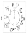
- FIG. 20 illustrates the usage examples of the above-described image sensor.
- the above-described image sensor can be used for, for example, various cases in which light such as visible light, infrared light, ultraviolet light, or X-rays is detected as follows.
- Devices that take images used for viewing such as a digital camera and a portable appliance with a camera function.
- Devices used for traffic such as an in-vehicle sensor that takes images of the front and the back of a car, surroundings, the inside of the car, and the like, a monitoring camera that monitors travelling vehicles and roads, and a distance sensor that measures distances between vehicles and the like, which are used for safe driving (e.g., automatic stop), recognition of the condition of a driver, and the like.
- safe driving e.g., automatic stop
- Devices used for home electrical appliances such as a TV, a refrigerator, and an air conditioner, to takes images of a gesture of a user and perform appliance operation in accordance with the gesture.
- Devices used for medical care and health care such as an endoscope and a device that performs angiography by reception of infrared light.
- Devices used for security such as a monitoring camera for crime prevention and a camera for personal authentication.
- Devices used for beauty care such as skin measurement equipment that takes images of the skin and a microscope that takes images of the scalp.
- Devices used for sports such as an action camera and a wearable camera for sports and the like.
- Devices used for agriculture such as a camera for monitoring the condition of the field and crops.
- embodiments of the present disclosure are not limited to the above-described embodiments, and various alterations may occur insofar as they are within the scope of the present disclosure.
- present technology may also be configured as below.
- a solid-state imaging device including:
- a vertical signal line configured to output a pixel signal of the pixel
- a clipping circuit configured to limit a voltage of the vertical signal line to a predetermined voltage
- the clipping circuit further includes a capacitor having one electrode connected to the gate of the transistor, and
- a voltage generation circuit configured to generate a plurality of different voltages is connected to the other electrode of the capacitor.
- the voltage generation circuit applies different voltages to the capacitor between in reading the reset level of the pixel and in reading a signal level of the pixel.
- the voltage generation circuit applies a first voltage to one capacitor in reading the reset level of the pixel, and applies a second voltage to another capacitor in reading a signal level of the pixel.
- the clipping circuit further includes a selector configured to turn on/off a limitation on the voltage of the vertical signal line using the predetermined voltage generated by the transistor.
- An electronic device including
- a vertical signal line configured to output a pixel signal of the pixel
- a clipping circuit configured to limit a voltage of the vertical signal line to a predetermined voltage
Landscapes
- Engineering & Computer Science (AREA)
- Multimedia (AREA)
- Signal Processing (AREA)
- Solid State Image Pick-Up Elements (AREA)
- Transforming Light Signals Into Electric Signals (AREA)
Abstract
Description
- The present technology relates to a solid-state imaging device and an electronic device, and particularly relates to a solid-state imaging device and an electronic device that enable a reduction in the voltage of an AD conversion circuit.
- Recent years have seen the widespread use of cameras using CMOS image sensors (solid-state imaging devices).
- In the case where such an image sensor is irradiated with high-intensity light, a phenomenon occurs in which a portion that originally is to be bright in an image becomes black. The black portion in the image is also called a sunspot etc., because it looks like a sunspot. The sunspot is caused by fluctuation of a reset level, which occurs when a large amount of charge generated in a photodiode (PD) constituting a pixel leaks to a floating diffusion (FD) or the FD is directly exposed to light.
- To correct such a sunspot, limiting the voltage of a vertical signal line so that the reset level does not fluctuate beyond a certain level has been proposed.
- For example, Patent Literature 1 describes that a clipping circuit limits the potential of a vertical signal line to different potentials between in reset level reading and in signal level reading.
- Patent Literature 1: JP 2012-85343A
- However, in the case where there is variation (mainly variation in threshold voltage) between amplification transistors of pixels, the reset level of a pixel fluctuates. Therefore, the gate voltage of the clipping circuit needs to be set to include some margin, in consideration of this variation. Accordingly, also a dynamic range of an AD conversion circuit needs to be set to include a margin similarly. That is, it is necessary to design the AD conversion circuit in consideration of at least a voltage corresponding to this margin, which hinders a reduction in the voltage of the AD conversion circuit.
- The present technology has been made in view of such circumstances, and enables a reduction in the voltage of an AD conversion circuit.
- A solid-state imaging device of an aspect of the present technology includes: a plurality of pixels; a vertical signal line configured to output a pixel signal of the pixel; and a clipping circuit configured to limit a voltage of the vertical signal line to a predetermined voltage. The clipping circuit includes a transistor configured to generate the predetermined voltage in accordance with a voltage of a gate, and a sample holding circuit configured to hold a reset level of the pixel that is output to the vertical signal line, and input the reset level to the gate of the transistor.
- The clipping circuit can further include a capacitor having one electrode connected to the gate of the transistor, and a voltage generation circuit configured to generate a plurality of different voltages can be connected to the other electrode of the capacitor.
- The voltage generation circuit can apply different voltages to the capacitor between in reading the reset level of the pixel and in reading a signal level of the pixel.
- The clipping circuit can include a plurality of the capacitors, and the voltage generation circuit can apply a first voltage to one capacitor in reading the reset level of the pixel, and apply a second voltage to another capacitor in reading a signal level of the pixel.
- The clipping circuit can further include a selector configured to turn on/off a limitation on the voltage of the vertical signal line using the predetermined voltage generated by the transistor.
- An electronic device of an aspect of the present technology includes a solid-state imaging device including a plurality of pixels, a vertical signal line configured to output a pixel signal of the pixel, and a clipping circuit configured to limit a voltage of the vertical signal line to a predetermined voltage. The clipping circuit includes a transistor configured to generate the predetermined voltage in accordance with a voltage of a gate, and a sample holding circuit configured to hold a reset level of the pixel that is output to the vertical signal line, and input the reset level to the gate of the transistor.
- In an aspect of the present technology, the predetermined voltage is generated in accordance with the voltage of the gate, and the reset level of the pixel that is output to the vertical signal line is held and input to the gate of the transistor.
- According to an aspect of the present technology, the voltage of an AD conversion circuit can be reduced.
-
FIG. 1 is a block diagram illustrating a configuration example of a solid-state imaging device of the present technology. -
FIG. 2 is a diagram for describing a structure of a solid-state imaging device. -
FIG. 3 illustrates a circuit configuration example of a solid-state imaging device of the present technology. -
FIG. 4 is a timing chart illustrating the operation of a solid-state imaging device of the present technology. -
FIG. 5 illustrates a circuit configuration example of a solid-state imaging device of the present technology. -
FIG. 6 is a timing chart illustrating the operation of a solid-state imaging device of the present technology. -
FIG. 7 illustrates a circuit configuration example of a conventional solid-state imaging device. -
FIG. 8 is a timing chart illustrating the operation of a conventional solid-state imaging device. -
FIG. 9 is a timing chart illustrating the operation of a conventional solid-state imaging device. -
FIG. 10 illustrates a circuit configuration example of a solid-state imaging device of a first embodiment. -
FIG. 11 is a timing chart illustrating the operation of the solid-state imaging device of the first embodiment. -
FIG. 12 illustrates a circuit configuration example of a solid-state imaging device of a second embodiment. -
FIG. 13 is a timing chart illustrating the operation of the solid-state imaging device of the second embodiment. -
FIG. 14 illustrates a circuit configuration example of a solid-state imaging device of a third embodiment. -
FIG. 15 illustrates a circuit configuration example of a solid-state imaging device of a fourth embodiment. -
FIG. 16 illustrates a circuit modification example of a configuration of a solid-state imaging device of the present technology. -
FIG. 17 illustrates a circuit modification example of a configuration of a solid-state imaging device of the present technology. -
FIG. 18 illustrates a circuit modification example of a configuration of a solid-state imaging device of the present technology. -
FIG. 19 is a block diagram illustrating a configuration example of an electronic device of the present technology. -
FIG. 20 illustrates usage examples of an image sensor. - Embodiments of the present technology are described below with reference to the drawings.
-
FIG. 1 is a block diagram illustrating a configuration example of a solid-state imaging device of the present technology. - A solid-state imaging device 1 is configured as a complementary metal oxide semiconductor (CMOS) image sensor. The solid-state imaging device 1 includes a pixel area (pixel array) 3 in which a plurality of
pixels 2 are regularly arranged in a two-dimensional array in a semiconductor substrate (e.g., a Si substrate), which is not illustrated, and a peripheral circuit unit. - The
pixel 2 includes a photoelectric conversion unit (e.g., a photodiode) and a plurality of pixel transistors (MOS transistors). The plurality of pixel transistors may include, for example, three transistors of a transfer transistor, a reset transistor, and an amplification transistor. Alternatively, the plurality of pixel transistors may include four transistors including a selection transistor in addition to the three transistors. - The
pixel 2 may be configured as one unit pixel, or may be in a pixel sharing structure. This pixel sharing structure is a structure in which a plurality of photodiodes share a floating diffusion and transistors other than a transfer transistor. - The peripheral circuit unit includes a
vertical drive circuit 4, column signal processing circuits 5, ahorizontal drive circuit 6, an output circuit 7, and acontrol circuit 8. - The
control circuit 8 receives an input clock and data commanding an operation mode or the like, and outputs data such as internal information of the solid-state imaging device 1. In addition, on the basis of a vertical synchronizing signal, a horizontal synchronizing signal, and a master clock, thecontrol circuit 8 generates a clock signal and a control signal that serve as a reference for the operation of thevertical drive circuit 4, the column signal processing circuits 5, thehorizontal drive circuit 6, and the like. Then, thecontrol circuit 8 inputs these signals to thevertical drive circuit 4, the column signal processing circuits 5, thehorizontal drive circuit 6, and the like. - The
vertical drive circuit 4 is constituted by a shift register, for example. Thevertical drive circuit 4 selects a pixel drive line, and supplies a pulse for driving pixels to the selected pixel drive line to drive pixels in units of rows. That is, thevertical drive circuit 4 selectively scans thepixels 2 of thepixel area 3 sequentially in the vertical direction in units of rows. Then, thevertical drive circuit 4 supplies pixel signals based on signal charge generated in accordance with the amount of received light in the photoelectric conversion units of therespective pixels 2 to the column signal processing circuits 5 through vertical signal lines 9. - The column signal processing circuit 5 is disposed for each column of the
pixels 2, for example. The column signal processing circuits 5 perform signal processing such as noise cancellation on signals output from thepixels 2 of one row, in units of pixel columns. Specifically, the column signal processing circuits 5 perform signal processing such as correlated double sampling (CDS) for cancelling fixed pattern noise peculiar to thepixel 2, signal amplification, and analog-digital (AD) conversion. In the output stage of the column signal processing circuit 5, a horizontal selection switch (not illustrated) is provided to be connected to ahorizontal signal line 10. - The
horizontal drive circuit 6 is constituted by a shift register, for example. Thehorizontal drive circuit 6 sequentially outputs a horizontal scanning pulse to select the column signal processing circuits 5 in order, and causes the column signal processing circuits 5 to output pixel signals to thehorizontal signal line 10. - The output circuit 7 performs signal processing on signals sequentially supplied from the column signal processing circuits 5 through the
horizontal signal line 10, and outputs the resulting signals. For example, the output circuit 7 performs only buffering in some cases, and performs black level adjustment, column variation correction, various digital signal processing, and the like in some cases. - Input/
output terminals 12 exchange signals with the outside. - Next, a structure of a solid-state imaging device to which the present technology is applied will be described.
- As a first example, a solid-state imaging device la illustrated in the upper stage of
FIG. 2 includes asemiconductor substrate 20. Thesemiconductor substrate 20 is equipped with apixel area 23, acontrol circuit 24, and alogic circuit 25 including a signal processing circuit. Thus, the solid-state imaging device 1 a is configured as one semiconductor chip. - As a second example, a solid-
state imaging device 1 b illustrated in the middle stage ofFIG. 2 includes afirst semiconductor substrate 21 and asecond semiconductor substrate 22. Thefirst semiconductor substrate 21 is equipped with thepixel area 23 and thecontrol circuit 24. Thesecond semiconductor substrate 22 is equipped with thelogic circuit 25 including a signal processing circuit. Thefirst semiconductor substrate 21 and thesecond semiconductor substrate 22 are electrically connected to each other to constitute the stacked-type solid-state imaging device 1 b serving as one semiconductor chip. - As a third example, a solid-
state imaging device 1 c illustrated in the lower stage ofFIG. 2 includes thefirst semiconductor substrate 21 and thesecond semiconductor substrate 22. Thefirst semiconductor substrate 21 is equipped with thepixel area 23. Thesecond semiconductor substrate 22 is equipped with thecontrol circuit 24 and thelogic circuit 25 including a signal processing circuit. Thefirst semiconductor substrate 21 and thesecond semiconductor substrate 22 are electrically connected to each other to constitute the stacked-type solid-state imaging device 1 c serving as one semiconductor chip. - Note that a configuration that electrically connects the
first semiconductor substrate 21 and thesecond semiconductor substrate 22 may be a through via, Cu—Cu metallic bonding, or other configurations. - In addition, the
second semiconductor substrate 22 includes one layer in the above description, but may include two or more layers. That is, the present technology is also applicable to a solid-state imaging device made of a stack of three or more layers including thefirst semiconductor substrate 21 as the uppermost layer. -
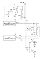
FIG. 3 illustrates a circuit configuration example of the solid-state imaging device 1 of the present technology. - As illustrated in
FIG. 3 , thepixel 2 includes a photodiode (PD) 51 serving as a photoelectric conversion unit, atransfer transistor 52, a floatingcapacitance 53, areset transistor 54, anamplification transistor 55, and aselection transistor 56. Note that all the pixel transistors included in thepixel 2 are configured as n-channel MOS transistors. - An anode of the
PD 51 is grounded, and a cathode of thePD 51 is connected to a source of thetransfer transistor 52. A drain of thetransfer transistor 52 is connected to a gate of theamplification transistor 55, and this connection point constitutes a floating diffusion (FD). - The
reset transistor 54 is connected between a predetermined power source and the FD. A drain of theamplification transistor 55 is connected to the predetermined power source, and a source of theamplification transistor 55 is connected to a drain of theselection transistor 56. A source of theselection transistor 56 is connected to avertical signal line 57. - In addition, the
vertical signal line 57 is connected to aload MOS transistor 58. Bias voltage generated by aBias generation circuit 59 is supplied to theload MOS transistor 58. Thus, theamplification transistor 55 and theload MOS transistor 58 constitute a source follower circuit. - The voltage of the vertical signal line 57 (a pixel signal) is read from an
output terminal 60. The output of theoutput terminal 60 is held by asample holding circuit 61 or asample holding circuit 62. Thesample holding circuit 61 holds the voltage (reset level) of thevertical signal line 57 corresponding to the potential of the FD when the FD is reset. Thesample holding circuit 62 holds the voltage (signal level) of thevertical signal line 57 corresponding to the potential of the FD when charge of thePD 51 is transferred to the FD. - Furthermore, a
clipping circuit 71 is connected to thevertical signal line 57. The clippingcircuit 71 limits (clips) the voltage of thevertical signal line 57 to a predetermined voltage. - The clipping
circuit 71 includes a clippingtransistor 81, asample holding circuit 82, and acapacitor 83. - The clipping
transistor 81 generates a voltage to limit the voltage of thevertical signal line 57, in accordance with a clipping voltage CLP applied to its gate. - The
sample holding circuit 82 holds the voltage of thevertical signal line 57, and inputs the voltage to the gate of the clippingtransistor 81. - One electrode of the
capacitor 83 is connected to the gate of the clippingtransistor 81. The other electrode of thecapacitor 83 is connected to a CLP adjustmentvoltage generation circuit 91. - The CLP adjustment
voltage generation circuit 91 generates an adjustment voltage VCLP for adjusting the clipping voltage CLP, and applies the adjustment voltage VCLP to thecapacitor 83. - Next, the operation of the solid-state imaging device illustrated in
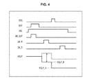
FIG. 3 will be described with reference to the timing chart ofFIG. 4 . - In
FIG. 4 , TRG is a drive signal for driving thetransfer transistor 52. RST is a drive signal for driving thereset transistor 54. SEL is a drive signal for driving theselection transistor 56. SH_CLP is a drive signal for driving thesample holding circuit 82. SH_R is a drive signal for driving thesample holding circuit 61. SH_S is a drive signal for driving thesample holding circuit 62. VCLP is an adjustment voltage for adjusting the clipping voltage CLP. - First, in a state where the drive signal SEL is high (H), when the drive signal RST rises to H, the FD of the
pixel 2 is reset. At this point, the drive signal SH_CLP rises to H; thus, the voltage (reset level) of thevertical signal line 57 is held and input to the gate of the clippingtransistor 81. - Then, when the drive signal SH_R rises to H, the
sample holding circuit 61 holds the reset level. That is, the reset level of thepixel 2 is read. - After that, when the drive signal TRG rises to H, charge of the
PD 51 is transferred to the FD of thepixel 2. - Then, when the drive signal SH_S rises to H, the
sample holding circuit 62 holds the voltage (signal level) of thevertical signal line 57 corresponding to the potential of the FD when charge of thePD 51 is transferred to the FD. That is, the signal level of thepixel 2 is read. - Here, the CLP adjustment
voltage generation circuit 91 applies different adjustment voltages VCLP to thecapacitor 83 between in reading the reset level of thepixel 2 and in reading the signal level of thepixel 2. - Specifically, the CLP adjustment
voltage generation circuit 91 applies an adjustment voltage VCLP_R to thecapacitor 83 in reading the reset level of thepixel 2. Thus, the clipping voltage CLP applied to the gate of the clippingtransistor 81 is adjusted, and the voltage of thevertical signal line 57 is limited to a first voltage. - In addition, the CLP adjustment
voltage generation circuit 91 applies an adjustment voltage VCLP_S lower than the adjustment voltage VCLP_R to thecapacitor 83 in reading the signal level of thepixel 2. Thus, the clipping voltage CLP applied to the gate of the clippingtransistor 81 is adjusted, and the voltage of thevertical signal line 57 is limited to a second voltage. - Note that as indicated by the dotted line in the drawing, the adjustment voltage VCLP_R and the adjustment voltage VCLP_S can be variable in accordance with the amount of adjustment of the clipping voltage CLP. The high-low relationship between the adjustment voltage VCLP_R and the adjustment voltage VCLP_S is reversed depending on the polarity of transistors included in the
pixel 2. - Such operation enables the reset level and the signal level to be clipped appropriately.
-
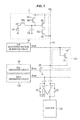
FIG. 5 illustrates another circuit configuration example of the solid-state imaging device 1 of the present technology. - The configuration in
FIG. 5 is basically similar to the configuration inFIG. 3 , but differs in that theclipping circuit 71 further includes aselector 111. - The
selector 111 turns on/off the limitation on the voltage of thevertical signal line 57 using a voltage generated by thetransistor 81. - Next, the operation of the solid-state imaging device illustrated in
FIG. 5 will be described with reference to the timing chart ofFIG. 6 . - In
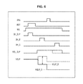
FIG. 6 , drive signals and adjustment voltages are similar to those illustrated inFIG. 4 , except for SEL_CLP. SEL_CLP is a drive signal for driving theselector 111. - As illustrated in
FIG. 6 , the drive signal SEL_CLP is in the H state in a period from the time of reading the reset level of thepixel 2 to the time of reading the signal level of thepixel 2. During this period, theselector 111 turns on the limitation on the voltage of thevertical signal line 57 using a voltage generated by thetransistor 81. - The operation in this case is similar to the operation described with reference to
FIG. 4 . - Here, as indicated by the dotted line in the drawing, the drive signal SEL_CLP is in the H state only in reading the reset level of the
pixel 2. During this period, theselector 111 turns on the limitation on the voltage of thevertical signal line 57 using a voltage generated by thetransistor 81. In reading the signal level, theselector 111 turns off the limitation on the voltage of thevertical signal line 57 using a voltage generated by thetransistor 81. - Such operation enables only the reset level to be clipped appropriately.
- Note that in the operation in
FIG. 6 , theselector 111 may turn off the limitation on the voltage of thevertical signal line 57 using a voltage generated by thetransistor 81, only in reading the signal level. Furthermore, the limitation on the voltage of thevertical signal line 57 may be turned on/off for each pixel column as necessary. - Here, a circuit configuration and operation of a conventional solid-state imaging device for correcting a sunspot will be described.
-
FIG. 7 illustrates a circuit configuration example of a conventional solid-state imaging device. The solid-state imaging device illustrated inFIG. 7 includes a single-slope AD conversion circuit. - In
FIG. 7 , aclipping circuit 121 includes the clippingtransistor 81. The clippingtransistor 81 generates a voltage to limit the voltage of thevertical signal line 57, in accordance with an adjustment voltage VCLP applied to its gate. - A
Ramp generation circuit 122 generates a reference signal Ramp that exhibits a ramp waveform having a predetermined slope at a predetermined timing. The reference signal Ramp is input to one terminal of acomparator 123. - The
comparator 123 compares the reference signal Ramp input to one terminal with a pixel signal input to the other terminal. Thecomparator 123 outputs a signal whose level is inverted in accordance with the magnitude relationship between the reference signal Ramp and the pixel signal to acounter 124. - The
counter 124 executes up-count operation and down-count operation while switching between them. Thecounter 124 ends the up-count operation and the down-count operation in accordance with a timing at which the output of thecomparator 123 is inverted. Count values obtained by the up-count operation and the down-count operation are output as digital data. - Note that the two terminals of the
comparator 123 are each configured in a manner that offset is cancelled (auto zero) by an AZ switch. - Thus, the
comparator 123 and thecounter 124 constitute a single-slope AD conversion circuit. - Next, the operation of the solid-state imaging device illustrated in
FIG. 7 will be described with reference to the timing chart ofFIG. 8 . - In
FIG. 8 , TRG is a drive signal for driving thetransfer transistor 52. RST is a drive signal for driving thereset transistor 54. SEL is a drive signal for driving theselection transistor 56. AZ is a drive signal for driving the AZ switches of thecomparator 123. VCLP is an adjustment voltage generated by the CLP adjustmentvoltage generation circuit 91. Ramp is a reference signal generated by theRamp generation circuit 122. VSL is the voltage of thevertical signal line 57, that is, a pixel signal. - Note that for VSL, the solid line indicates a pixel signal in a state (dark) where charge of the PD does not leak to the FD. The dotted line indicates a pixel signal in a state (light) where charge of the PD leaks to the FD and a sunspot occurs.
- Although detailed description of signals will be omitted, the CLP adjustment
voltage generation circuit 91 applies different adjustment voltages VCLP to the gate of thetransistor 81 between in reading the reset level of thepixel 2 and in reading the signal level of thepixel 2. Such operation enables the reset level and the signal level to be clipped appropriately. - Here, attention is focused on a dark pixel signal and a light pixel signal (VSL).
- In reset level reading, a voltage difference Va between the dark pixel signal and the light pixel signal exhibits a voltage difference equal to or more than a voltage difference that does not interfere with a normal pixel. Furthermore, a voltage difference Vb between in reset level reading and in signal level reading of the light pixel signal exhibits a voltage difference by which it can be determined that a sunspot has occurred.
- In this case, a sum Vdr of the voltage difference Va and the voltage difference Vb is needed as a dynamic range of the AD conversion circuit.
- However, in the case where there is variation (mainly variation in threshold voltage) between amplification transistors of pixels, the reset level of a pixel (dark) fluctuates as illustrated in
FIG. 9 . Therefore, the gate voltage of thetransistor 81 of theclipping circuit 121 needs to be set to include some margin, in consideration of this variation. Accordingly, also the dynamic range Vdr of the AD conversion circuit needs to be set to include a margin similarly. That is, it is necessary to design the AD conversion circuit in consideration of at least a voltage corresponding to this margin. - Hence, in a solid-state imaging device of the present technology, a reset level is held and input to the gate of the clipping
transistor 81. -
FIG. 10 illustrates a circuit configuration example of a solid-state imaging device of a first embodiment of the present technology. The solid-state imaging device illustrated inFIG. 10 includes a single-slope AD conversion circuit. - The solid-state imaging device illustrated in
FIG. 10 includes, as a clipping circuit, the clippingcircuit 71 described with reference toFIG. 3 . - With this configuration, as illustrated in
FIG. 11 , in the case where a reset level of a pixel (dark) fluctuates, a reset level including variation is held by the gate of the clippingtransistor 81. That is, there is no need to provide a margin in consideration of this variation for the gate voltage of thetransistor 81 of theclipping circuit 71. Accordingly, there also is no need to provide a margin similarly for the dynamic range Vdr of the AD conversion circuit. Consequently, the AD conversion circuit can be designed with the minimum dynamic range, without taking into consideration a voltage corresponding to this margin. As a result, the voltage of the AD conversion circuit can be reduced. -
FIG. 12 illustrates a circuit configuration example of a solid-state imaging device of a second embodiment of the present technology. The solid-state imaging device illustrated inFIG. 12 also includes a single-slope AD conversion circuit. - The solid-state imaging device illustrated in
FIG. 12 includes, as a clipping circuit, the clippingcircuit 71 described with reference toFIG. 5 . - With this configuration, as illustrated in
FIG. 13 , in the case where a reset level of a pixel (dark) fluctuates, a reset level including variation is held by the gate of the clippingtransistor 81. That is, there is no need to provide a margin in consideration of this variation for the gate voltage of thetransistor 81 of theclipping circuit 71. Accordingly, there also is no need to provide a margin similarly for the dynamic range Vdr of the AD conversion circuit. Consequently, the AD conversion circuit can be designed with the minimum dynamic range, without taking into consideration a voltage corresponding to this margin. As a result, the voltage of the AD conversion circuit can be reduced. - Note that in the operation in
FIG. 13 , theselector 111 may turn off the limitation on the voltage of thevertical signal line 57 using a voltage generated by thetransistor 81, only in reset level reading or only in signal level reading. Furthermore, the limitation on the voltage of thevertical signal line 57 may be turned on/off for each pixel column as necessary. -
FIG. 14 illustrates a circuit configuration example of a solid-state imaging device of a third embodiment of the present technology. - The solid-state imaging device illustrated in
FIG. 14 includes, in addition to the configuration inFIG. 12 , again amplifier 131 preceding thecomparator 123. - The
gain amplifier 131 amplifies the voltage of thevertical signal line 57, that is, a pixel signal, and supplies the amplified voltage to thecomparator 123. - Also in the configuration illustrated in
FIG. 14 , actions and effects equivalent to those of the configuration inFIG. 10 and the configuration inFIG. 12 can be obtained. -
FIG. 15 illustrates a circuit configuration example of a solid-state imaging device of a fourth embodiment of the present technology. - The solid-state imaging device illustrated in
FIG. 15 includes, in place of thecapacitor 83 of theclipping circuit 71 in the configuration inFIG. 12 , two capacitors 83-R and 83-S. - One electrode of each of the capacitors 83-R and 83-S is connected to the gate of the clipping
transistor 81. The other electrode of eachcapacitor 83 is connected to a CLP adjustmentvoltage generation circuit 141. - The CLP adjustment
voltage generation circuit 141 generates an adjustment voltage VCLP_R and applies it to the capacitor 83-R in reading the reset level of thepixel 2. In addition, the CLP adjustmentvoltage generation circuit 141 generates an adjustment voltage VCLP_S lower than the adjustment voltage VCLP_R and applies it to the capacitor 83-S in reading the signal level of thepixel 2. - Such operation enables the reset level and the signal level to be clipped appropriately.
- Also in the configuration illustrated in
FIG. 15 , actions and effects equivalent to those of the configuration inFIG. 10 and the configuration inFIG. 12 can be obtained. - Incidentally, as described with reference to
FIG. 2 , a solid-state imaging device of the present technology can have a stacked structure. - In this case, as illustrated in
FIG. 16 , the clippingcircuit 71 may be provided not in thefirst semiconductor substrate 21 including the pixels 2 (the pixel area 23) but in thesecond semiconductor substrate 22 including thelogic circuit 25. - Conversely, as illustrated in
FIG. 17 , the clippingcircuit 71 may be provided not in thesecond semiconductor substrate 22 including thelogic circuit 25 but in thefirst semiconductor substrate 21 including the pixels 2 (the pixel area 23). - Furthermore, in the circuit configurations of the solid-state imaging devices described above, the clipping circuit may be provided at any position.
- For example, as illustrated in
FIG. 18 , the clippingcircuit 71 may be provided to follow theload MOS transistor 58. - The present technology is not limited to application to solid-state imaging devices, and is also applicable to imaging devices. Here, imaging devices refer to a camera system (e.g., a digital still camera and a digital video camera) and an electronic device with an imaging function (e.g., a mobile phone). Note that a module form mounted on an electronic device, that is, a camera module, is taken as an imaging device in some cases.
- Here, a configuration example of an electronic device to which the present technology is applied will be described, with reference to
FIG. 19 . - An
electronic device 200 illustrated inFIG. 19 includes anoptical lens 201, ashutter device 202, a solid-state imaging device 203, adrive circuit 204, and asignal processing circuit 205.FIG. 19 illustrates an embodiment in which the solid-state imaging device 1 of the present technology described above is provided in an electronic device (digital still camera) as the solid-state imaging device 203. - The
optical lens 201 causes image light (incident light) from an object to form an image on an imaging surface of the solid-state imaging device 203. Thus, signal charge is accumulated in the solid-state imaging device 203 for a certain period. Theshutter device 202 controls a light irradiation period and a light blocking period for the solid-state imaging device 203. - The
drive circuit 204 supplies drive signals to theshutter device 202 and the solid-state imaging device 203. The drive signal supplied to theshutter device 202 is a signal for controlling shutter operation of theshutter device 202. The drive signal supplied to the solid-state imaging device 203 is a signal for controlling signal transfer operation of the solid-state imaging device 203. The solid-state imaging device 203 performs signal transfer in accordance with the drive signal (timing signal) supplied from thedrive circuit 204. Thesignal processing circuit 205 performs various signal processing on signals output from the solid-state imaging device 203. Video signals that have undergone signal processing are stored in a storage medium, such as a memory, or output to a monitor. - In the
electronic device 200 of the present embodiment, the voltage of an AD conversion circuit can be reduced in the solid-state imaging device 203; thus, as a result, an electronic device with low power consumption can be provided. - Lastly, usage examples of the image sensor to which the present technology is applied will be described.
-
FIG. 20 illustrates the usage examples of the above-described image sensor. - The above-described image sensor can be used for, for example, various cases in which light such as visible light, infrared light, ultraviolet light, or X-rays is detected as follows.
- Devices that take images used for viewing, such as a digital camera and a portable appliance with a camera function.
- Devices used for traffic, such as an in-vehicle sensor that takes images of the front and the back of a car, surroundings, the inside of the car, and the like, a monitoring camera that monitors travelling vehicles and roads, and a distance sensor that measures distances between vehicles and the like, which are used for safe driving (e.g., automatic stop), recognition of the condition of a driver, and the like.
- Devices used for home electrical appliances, such as a TV, a refrigerator, and an air conditioner, to takes images of a gesture of a user and perform appliance operation in accordance with the gesture.
- Devices used for medical care and health care, such as an endoscope and a device that performs angiography by reception of infrared light.
- Devices used for security, such as a monitoring camera for crime prevention and a camera for personal authentication.
- Devices used for beauty care, such as skin measurement equipment that takes images of the skin and a microscope that takes images of the scalp.
- Devices used for sports, such as an action camera and a wearable camera for sports and the like.
- Devices used for agriculture, such as a camera for monitoring the condition of the field and crops.
- In addition, embodiments of the present disclosure are not limited to the above-described embodiments, and various alterations may occur insofar as they are within the scope of the present disclosure.
- Additionally, the present technology may also be configured as below.
- (1)
- A solid-state imaging device including:
- a plurality of pixels;
- a vertical signal line configured to output a pixel signal of the pixel; and
- a clipping circuit configured to limit a voltage of the vertical signal line to a predetermined voltage,
- in which the clipping circuit includes
-
- a transistor configured to generate the predetermined voltage in accordance with a voltage of a gate, and
- a sample holding circuit configured to hold a reset level of the pixel that is output to the vertical signal line, and input the reset level to the gate of the transistor.
(2)
- The solid-state imaging device according to (1),
- in which the clipping circuit further includes a capacitor having one electrode connected to the gate of the transistor, and
- a voltage generation circuit configured to generate a plurality of different voltages is connected to the other electrode of the capacitor.
- (3)
- The solid-state imaging device according to (2),
- in which the voltage generation circuit applies different voltages to the capacitor between in reading the reset level of the pixel and in reading a signal level of the pixel.
- (4)
- The solid-state imaging device according to (2),
- the voltage generation circuit applies a first voltage to one capacitor in reading the reset level of the pixel, and applies a second voltage to another capacitor in reading a signal level of the pixel.
- (5)
- The solid-state imaging device according to any one of (1) to (4),
- in which the clipping circuit further includes a selector configured to turn on/off a limitation on the voltage of the vertical signal line using the predetermined voltage generated by the transistor.
- (6)
- An electronic device including
- a solid-state imaging device including
- a plurality of pixels,
- a vertical signal line configured to output a pixel signal of the pixel, and
- a clipping circuit configured to limit a voltage of the vertical signal line to a predetermined voltage,
- in which the clipping circuit includes
-
- a transistor configured to generate the predetermined voltage in accordance with a voltage of a gate, and
- a sample holding circuit configured to hold a reset level of the pixel that is output to the vertical signal line, and input the reset level to the gate of the transistor.
-
- 1 solid-state imaging device
- 2 pixel
- 57 vertical signal line
- 71 clipping circuit
- 81 clipping transistor
- 82 sample holding circuit
- 83 capacitor
- 91 CLP adjustment voltage generation circuit
- 111 selector
- 200 electronic device
- 203 solid-state imaging device
Claims (6)
Applications Claiming Priority (3)
| Application Number | Priority Date | Filing Date | Title |
|---|---|---|---|
| JP2015076732 | 2015-04-03 | ||
| JP2015-076732 | 2015-04-03 | ||
| PCT/JP2016/058649 WO2016158484A1 (en) | 2015-04-03 | 2016-03-18 | Solid-state imaging device and electronic instrument |
Publications (2)
| Publication Number | Publication Date |
|---|---|
| US20180098005A1 true US20180098005A1 (en) | 2018-04-05 |
| US10171761B2 US10171761B2 (en) | 2019-01-01 |
Family
ID=57005795
Family Applications (1)
| Application Number | Title | Priority Date | Filing Date |
|---|---|---|---|
| US15/560,645 Active US10171761B2 (en) | 2015-04-03 | 2016-03-18 | Solid-state imaging device and electronic device |
Country Status (2)
| Country | Link |
|---|---|
| US (1) | US10171761B2 (en) |
| WO (1) | WO2016158484A1 (en) |
Cited By (6)
| Publication number | Priority date | Publication date | Assignee | Title |
|---|---|---|---|---|
| US10462396B2 (en) * | 2017-06-01 | 2019-10-29 | Panasonic Intellectual Property Management Co., Ltd. | Imaging device |
| US20210014444A1 (en) * | 2019-07-10 | 2021-01-14 | Semiconductor Components Industries, Llc | Image sensors with in-pixel amplification circuitry |
| EP3828509A4 (en) * | 2018-07-26 | 2022-04-27 | Boe Technology Group Co., Ltd. | Light detecting circuit and electronic device, driving method, and optical recognition method and apparatus |
| US20220337776A1 (en) * | 2019-09-30 | 2022-10-20 | Nikon Corporation | Imaging element and imaging device |
| US20220385844A1 (en) * | 2019-09-30 | 2022-12-01 | Nikon Corporation | Imaging element and imaging device |
| US11800253B2 (en) | 2020-05-15 | 2023-10-24 | Canon Kabushiki Kaisha | Imaging device and imaging system |
Families Citing this family (3)
| Publication number | Priority date | Publication date | Assignee | Title |
|---|---|---|---|---|
| WO2020073626A1 (en) * | 2018-10-09 | 2020-04-16 | Shenzhen GOODIX Technology Co., Ltd. | Image sensor with dynamic charge-domain sampling |
| JP7345301B2 (en) * | 2019-07-18 | 2023-09-15 | キヤノン株式会社 | Photoelectric conversion devices and equipment |
| US20260107076A1 (en) * | 2022-08-25 | 2026-04-16 | Sony Semiconductor Solutions Corporation | Imaging device |
Citations (1)
| Publication number | Priority date | Publication date | Assignee | Title |
|---|---|---|---|---|
| US7741593B2 (en) * | 2008-02-13 | 2010-06-22 | Canon Kabushiki Kaisha | Photoelectric conversion device and imaging system |
Family Cites Families (3)
| Publication number | Priority date | Publication date | Assignee | Title |
|---|---|---|---|---|
| JP5340374B2 (en) | 2005-06-09 | 2013-11-13 | キヤノン株式会社 | Imaging apparatus and imaging system |
| JP2006352341A (en) | 2005-06-14 | 2006-12-28 | Micron Technol Inc | Anti-Eclipse circuit and its operation method |
| JP2008042676A (en) | 2006-08-08 | 2008-02-21 | Canon Inc | Photoelectric conversion device and photoelectric conversion system |
-
2016
- 2016-03-18 US US15/560,645 patent/US10171761B2/en active Active
- 2016-03-18 WO PCT/JP2016/058649 patent/WO2016158484A1/en not_active Ceased
Patent Citations (1)
| Publication number | Priority date | Publication date | Assignee | Title |
|---|---|---|---|---|
| US7741593B2 (en) * | 2008-02-13 | 2010-06-22 | Canon Kabushiki Kaisha | Photoelectric conversion device and imaging system |
Cited By (11)
| Publication number | Priority date | Publication date | Assignee | Title |
|---|---|---|---|---|
| US10462396B2 (en) * | 2017-06-01 | 2019-10-29 | Panasonic Intellectual Property Management Co., Ltd. | Imaging device |
| US11019289B2 (en) | 2017-06-01 | 2021-05-25 | Panasonic Intellectual Property Management Co., Ltd. | Imaging device |
| EP3828509A4 (en) * | 2018-07-26 | 2022-04-27 | Boe Technology Group Co., Ltd. | Light detecting circuit and electronic device, driving method, and optical recognition method and apparatus |
| US11334194B2 (en) | 2018-07-26 | 2022-05-17 | Boe Technology Group Co., Ltd. | Light detection circuit, electronic device, and optical recognition method |
| US20210014444A1 (en) * | 2019-07-10 | 2021-01-14 | Semiconductor Components Industries, Llc | Image sensors with in-pixel amplification circuitry |
| US10958861B2 (en) * | 2019-07-10 | 2021-03-23 | Semiconductor Components Industries, Llc | Image sensors with in-pixel amplification circuitry |
| US20220337776A1 (en) * | 2019-09-30 | 2022-10-20 | Nikon Corporation | Imaging element and imaging device |
| US20220385844A1 (en) * | 2019-09-30 | 2022-12-01 | Nikon Corporation | Imaging element and imaging device |
| US12244955B2 (en) * | 2019-09-30 | 2025-03-04 | Nikon Corporation | Imaging element and imaging device |
| US12273640B2 (en) * | 2019-09-30 | 2025-04-08 | Nikon Corporation | Imaging element and imaging device |
| US11800253B2 (en) | 2020-05-15 | 2023-10-24 | Canon Kabushiki Kaisha | Imaging device and imaging system |
Also Published As
| Publication number | Publication date |
|---|---|
| US10171761B2 (en) | 2019-01-01 |
| WO2016158484A1 (en) | 2016-10-06 |
Similar Documents
| Publication | Publication Date | Title |
|---|---|---|
| US10171761B2 (en) | Solid-state imaging device and electronic device | |
| US11050955B2 (en) | Solid-state imaging device, method for driving solid-state imaging device, and electronic apparatus | |
| US11228726B2 (en) | Solid-state imaging device, control method thereof, and electronic apparatus | |
| US9900537B2 (en) | Solid-state imaging unit and electronic apparatus with a signal charge accumulated in a photoelectric conversion section that is divided to be read in predetermined times of intermediate transfer operations and a complete transfer operation | |
| US11765481B2 (en) | Imaging element, photodetector element, and electronic equipment with a threshold that is randomly varied for an analog-to-digital converter | |
| US9473720B2 (en) | Solid-state image-capturing device and image-capturing device | |
| US10811447B2 (en) | Solid-state imaging device, driving method, and electronic equipment | |
| JP2021057795A (en) | Solid-state image pickup device, driving method of the solid-state image pickup device, and electronic apparatus | |
| US10841517B2 (en) | Solid-state imaging device and imaging system | |
| US11153518B2 (en) | Solid-state imaging element and imaging apparatus | |
| US8023022B2 (en) | Solid-state imaging apparatus | |
| US10412329B2 (en) | Imaging apparatus with logarithmic characteristics and method for driving the same | |
| US10186512B2 (en) | Solid-state image sensor, image capturing device, and electronic device | |
| US10446603B2 (en) | Imaging element, driving method of imaging element, and electronic device | |
| US10757350B2 (en) | Solid-state image pickup device and electronic apparatus | |
| US11463645B2 (en) | Solid-state imaging element and electronic device including a shared structure for pixels for sharing an AD converter | |
| WO2020111100A1 (en) | Solid-state imaging device and electronic device | |
| US20170026591A1 (en) | Image sensor | |
| US11463638B2 (en) | Streaking correction circuit, imaging apparatus, and electronic equipment | |
| US10348991B2 (en) | Solid-state image pickup device with load transistors, method for controlling the same, and electronic apparatus | |
| US10694132B2 (en) | Solid-state imaging device, signal processing method, and electronic device |
Legal Events
| Date | Code | Title | Description |
|---|---|---|---|
| AS | Assignment |
Owner name: SONY CORPORATION, JAPAN Free format text: ASSIGNMENT OF ASSIGNORS INTEREST;ASSIGNOR:HANZAWA, KATSUHIKO;REEL/FRAME:043973/0889 Effective date: 20170810 |
|
| FEPP | Fee payment procedure |
Free format text: ENTITY STATUS SET TO UNDISCOUNTED (ORIGINAL EVENT CODE: BIG.); ENTITY STATUS OF PATENT OWNER: LARGE ENTITY |
|
| STCF | Information on status: patent grant |
Free format text: PATENTED CASE |
|
| MAFP | Maintenance fee payment |
Free format text: PAYMENT OF MAINTENANCE FEE, 4TH YEAR, LARGE ENTITY (ORIGINAL EVENT CODE: M1551); ENTITY STATUS OF PATENT OWNER: LARGE ENTITY Year of fee payment: 4 |