US20180046292A1 - Touch sensor-equipped display device - Google Patents
Touch sensor-equipped display device Download PDFInfo
- Publication number
- US20180046292A1 US20180046292A1 US15/553,569 US201615553569A US2018046292A1 US 20180046292 A1 US20180046292 A1 US 20180046292A1 US 201615553569 A US201615553569 A US 201615553569A US 2018046292 A1 US2018046292 A1 US 2018046292A1
- Authority
- US
- United States
- Prior art keywords
- slits
- display
- substrate
- touch sensor
- arrangement interval
- Prior art date
- Legal status (The legal status is an assumption and is not a legal conclusion. Google has not performed a legal analysis and makes no representation as to the accuracy of the status listed.)
- Abandoned
Links
Images


Classifications
-
- G—PHYSICS
- G06—COMPUTING OR CALCULATING; COUNTING
- G06F—ELECTRIC DIGITAL DATA PROCESSING
- G06F3/00—Input arrangements for transferring data to be processed into a form capable of being handled by the computer; Output arrangements for transferring data from processing unit to output unit, e.g. interface arrangements
- G06F3/01—Input arrangements or combined input and output arrangements for interaction between user and computer
- G06F3/03—Arrangements for converting the position or the displacement of a member into a coded form
- G06F3/041—Digitisers, e.g. for touch screens or touch pads, characterised by the transducing means
- G06F3/0412—Digitisers structurally integrated in a display
-
- G—PHYSICS
- G06—COMPUTING OR CALCULATING; COUNTING
- G06F—ELECTRIC DIGITAL DATA PROCESSING
- G06F3/00—Input arrangements for transferring data to be processed into a form capable of being handled by the computer; Output arrangements for transferring data from processing unit to output unit, e.g. interface arrangements
- G06F3/01—Input arrangements or combined input and output arrangements for interaction between user and computer
- G06F3/03—Arrangements for converting the position or the displacement of a member into a coded form
- G06F3/041—Digitisers, e.g. for touch screens or touch pads, characterised by the transducing means
- G06F3/0416—Control or interface arrangements specially adapted for digitisers
- G06F3/04166—Details of scanning methods, e.g. sampling time, grouping of sub areas or time sharing with display driving
-
- G—PHYSICS
- G06—COMPUTING OR CALCULATING; COUNTING
- G06F—ELECTRIC DIGITAL DATA PROCESSING
- G06F3/00—Input arrangements for transferring data to be processed into a form capable of being handled by the computer; Output arrangements for transferring data from processing unit to output unit, e.g. interface arrangements
- G06F3/01—Input arrangements or combined input and output arrangements for interaction between user and computer
- G06F3/03—Arrangements for converting the position or the displacement of a member into a coded form
- G06F3/041—Digitisers, e.g. for touch screens or touch pads, characterised by the transducing means
- G06F3/044—Digitisers, e.g. for touch screens or touch pads, characterised by the transducing means by capacitive means
- G06F3/0445—Digitisers, e.g. for touch screens or touch pads, characterised by the transducing means by capacitive means using two or more layers of sensing electrodes, e.g. using two layers of electrodes separated by a dielectric layer
-
- G—PHYSICS
- G06—COMPUTING OR CALCULATING; COUNTING
- G06F—ELECTRIC DIGITAL DATA PROCESSING
- G06F3/00—Input arrangements for transferring data to be processed into a form capable of being handled by the computer; Output arrangements for transferring data from processing unit to output unit, e.g. interface arrangements
- G06F3/01—Input arrangements or combined input and output arrangements for interaction between user and computer
- G06F3/03—Arrangements for converting the position or the displacement of a member into a coded form
- G06F3/041—Digitisers, e.g. for touch screens or touch pads, characterised by the transducing means
- G06F3/044—Digitisers, e.g. for touch screens or touch pads, characterised by the transducing means by capacitive means
- G06F3/0446—Digitisers, e.g. for touch screens or touch pads, characterised by the transducing means by capacitive means using a grid-like structure of electrodes in at least two directions, e.g. using row and column electrodes
-
- G—PHYSICS
- G06—COMPUTING OR CALCULATING; COUNTING
- G06F—ELECTRIC DIGITAL DATA PROCESSING
- G06F3/00—Input arrangements for transferring data to be processed into a form capable of being handled by the computer; Output arrangements for transferring data from processing unit to output unit, e.g. interface arrangements
- G06F3/01—Input arrangements or combined input and output arrangements for interaction between user and computer
- G06F3/03—Arrangements for converting the position or the displacement of a member into a coded form
- G06F3/041—Digitisers, e.g. for touch screens or touch pads, characterised by the transducing means
- G06F3/044—Digitisers, e.g. for touch screens or touch pads, characterised by the transducing means by capacitive means
- G06F3/0448—Details of the electrode shape, e.g. for enhancing the detection of touches, for generating specific electric field shapes, for enhancing display quality
Definitions
- the present invention relates to a touch sensor-equipped display device.
- Patent Document 1 discloses a touch sensor-equipped display device that includes touch drive electrodes and touch detection electrodes.
- slits are provided in the touch detection electrodes so that the touch detection electrodes become unnoticeable to human eye.
- a touch sensor-equipped display device in one embodiment of the present invention includes: a display panel including a first substrate, a second substrate opposed to the first substrate, and a display function layer interposed between the first substrate and the second substrate, the display function layer including a plurality of display pixels arranged in matrix; a touch drive electrode that is provided between the first substrate and the second substrate and extends in a first direction; and a touch detection electrode that is provided on a surface of the first substrate on a side opposite to the touch drive electrode, and extends in a second direction that intersects with the first direction at a right angle.
- a plurality of slits each of which is repeatedly bent in a zigzag shape while extending in the second direction are provided in the touch detection electrode so as to be arrayed in the first direction; an arrangement interval “a” for the slits adjacent in the first direction satisfies relationship given as:
- a turnback width of the slits in the zigzag shape is set to (a distance between centers of subpixels adjacent in the first direction among subpixels composing one display pixel) ⁇ a natural number equal to or greater than (the number of colors of the subpixels+1) ⁇ .
- the present invention the occurrence of moire caused by the interference between the array pattern of subpixels and the pattern of the slits in the touch detection electrode can be suppressed, whereby the display quality of the display device can be improved.
- FIG. 1 illustrates a cross-sectional configuration of a touch sensor-equipped display device in one embodiment.
- FIG. 2 is a plan view illustrating the touch sensor-equipped display device in one embodiment.
- FIG. 3 is a schematic cross-sectional view of a liquid crystal panel with a touch sensor function.
- FIG. 4 is an enlarged plan view illustrating a plan-view configuration in a display section of an array substrate that composes the liquid crystal panel with a touch sensor function.
- FIG. 5 is an enlarged plan view illustrating a plan-view configuration in a display section of a CF substrate that composes the liquid crystal panel with a touch sensor function.
- FIG. 6 is a plan view illustrating an arrangement configuration of touch drive electrodes and touch detection electrodes.
- FIG. 7 is a diagram for explaining a shape of a slit provided in touch detection electrodes.
- FIG. 8 illustrates one exemplary arrangement of color filters.
- FIG. 9 is a diagram obtained by superposing the diagram of the touch detection electrode configuration illustrated in FIG. 7 on the diagram of color filter arrangement illustrated in FIG. 8 .
- FIG. 10A is an enlarged view illustrating a part of the display screen when the entirety of the display screen is in a white color display state, in a case where the arrangement interval “a” for the slits is set to 1.000 time the arrangement interval “b” for the display pixels.
- FIG. 10B is an enlarged view illustrating a part of the display screen when the entirety of the display screen is in a white color display state, in a case where the arrangement interval “a” for the slits is set to 1.225 times the arrangement interval “b” for the display pixels.
- FIG. 10C is an enlarged view illustrating a part of the display screen when the entirety of the display screen is in a white color display state, in a case where the arrangement interval “a” for the slits is set to 1.250 times the arrangement interval “b” for the display pixels.
- FIG. 10D is an enlarged view illustrating a part of the display screen when the entirety of the display screen is in a white color display state, in a case where the arrangement interval “a” for the slits is set to 1.500 times the arrangement interval “b” for the display pixels.
- FIG. 10E is an enlarged view illustrating a part of the display screen when the entirety of the display screen is in a white color display state, in a case where the arrangement interval “a” for the slits is set to 1.725 times the arrangement interval “b” for the display pixels.
- FIG. 10F is an enlarged view illustrating a part of the display screen when the entirety of the display screen is in a white color display state, in a case where the arrangement interval “a” for the slits is set to 2.000 times the arrangement interval “b” for the display pixels.
- FIG. 11A is an enlarged view illustrating a part of the display screen when a black-and-white vertical stripe display is performed, in a case where the arrangement interval “a” for the slits is set to 1.725 times the arrangement interval “b” for the display pixels.
- FIG. 11B is an enlarged view illustrating a part of the display screen when a black-and-white chessboard pattern display is performed, in a case where the arrangement interval “a” for the slits is set to 1.725 times the arrangement interval “b” for the display pixels.
- FIG. 11C is an enlarged view illustrating a part of the display screen when an RCSB chessboard pattern display is performed, in a case where the arrangement interval “a” for the slits is set to 1.725 times the arrangement interval “b” for the display pixels.
- FIG. 12A is a diagram for explaining a method for displaying a black-and-white vertical stripe display.
- FIG. 12B is a diagram for explaining a black-and-white chessboard pattern display.
- FIG. 12C is a diagram for explaining a black-and-white chessboard pattern display.
- a touch sensor-equipped display device in one embodiment of the present invention includes: a display panel including a first substrate, a second substrate opposed to the first substrate, arid a display function layer interposed between the first substrate and the second substrate, the display function layer including a plurality of display pixels arranged in matrix; a touch drive electrode that is provided between the first substrate and the second substrate and extends in a first direction; and a touch detection electrode that is provided on a surface of the first substrate on a side opposite to the touch drive electrode, and extends in a second direction that intersects with the first direction at a right angle.
- a plurality of slits each of which is repeatedly bent in a zigzag shape while extending in the second direction are provided in the touch detection electrode so as to be arrayed in the first direction; an arrangement interval “a” for the slits adjacent in the first direction satisfies relationship given as:
- a turnback width of the slits in the zigzag shape is set to (a distance between centers of subpixels adjacent in the first direction among subpixels composing one display pixel) ⁇ a natural number equal to or greater than (the number of colors of the subpixels +1) ⁇ (the first configuration).
- the occurrence of moire caused by the interference between the array pattern of subpixels and the pattern of the slits in the touch detection electrode can be suppressed, whereby the display quality of the display device can be improved.
- the slits In the first configuration, the slits have a width of 20 ⁇ m or less (the second configuration).
- the occurrence of moire can be suppressed, whereby the display quality of the display device can be improved.
- the arrangement interval “a” for the slits is 175 ⁇ m or less (the third configuration).
- the occurrence of moire can be suppressed, whereby the display quality of the display device can be improved.
- the angle ⁇ for the slits is in a range of 25° to 45° (the fourth configuration).
- the occurrence of moire can be suppressed, whereby the display quality of the display device can be improved.
- FIG. 1 illustrates a cross-sectional configuration of a touch sensor-equipped display device 10 in one embodiment.
- FIG. 2 is a plan view illustrating the touch sensor-equipped display device 10 in one embodiment.
- the touch sensor-equipped display device 10 includes a liquid crystal panel 11 with a touch sensor function, a backlight device (lighting device) 13 , a bezel 14 , a case 15 , and a cover 16 .
- the side thereof on which the cover 16 is provided is the front side
- the side thereof on which the case 15 is provided is the rear side.
- the liquid crystal panel 11 with a touch sensor function has a function of displaying an image, and a touch sensor function of detecting a touched position. More specifically, the liquid crystal panel 11 with a touch sensor function has a configuration that includes: a liquid crystal panel (display panel) that includes a pair of substrates and a display function layer provided between the substrates, the display function layer including a plurality of display pixels provided in matrix; touch drive electrodes provided between the pair of substrates of the liquid crystal panel; and touch detection electrodes provided on a front side of the substrate on the front side of the display panel.
- a liquid crystal panel display panel
- the display function layer including a plurality of display pixels provided in matrix
- touch drive electrodes provided between the pair of substrates of the liquid crystal panel
- touch detection electrodes provided on a front side of the substrate on the front side of the display panel.
- the backlight device 13 is an external light source that emits light toward the liquid crystal panel 11 with a touch sensor function.
- the cover 16 is arranged on an outer side of the liquid crystal panel 11 with a touch sensor function so as to protect the liquid crystal panel 11 with a touch sensor function.
- This cover 16 is made of a material that has excellent impact resistance, for example, tempered glass.
- the liquid crystal panel 11 with a touch sensor function, and the cover 16 are bonded and integrated with each other with an approximately transparent adhesive (not shown) being interposed therebetween.
- the bezel 14 holds the cover 16 and the liquid crystal panel 11 with a touch sensor function together, between the same and the backlight device 13 .
- the bezel 14 is attached to the case 15 , and the case 15 houses the backlight device 13 .
- FIG. 3 is a schematic cross-sectional view of the liquid crystal panel 11 with a touch sensor function.
- FIG. 4 is an enlarged plan view illustrating a plan-view configuration in a display section of an array substrate that composes the liquid crystal panel 11 with a touch sensor function.
- FIG. 5 is an enlarged plan view illustrating a plan-view configuration in a display section of a CF substrate that composes the liquid crystal panel 11 with a touch sensor function.
- the liquid crystal panel 11 with a touch sensor function includes a pair of substrates 11 a and 11 b that are transparent (that have excellent translucency), and a liquid crystal layer 11 c interposed between the substrates 11 a and 11 b , as illustrated in FIG. 3 .
- the liquid crystal layer 11 c contains liquid crystal molecules as a substance whose optical properties change in response to the application of an electric field.
- the substrates 11 a and 11 b are bonded with each other with a sealant (not shown) in a state in which a cell gap corresponding to the thickness of the liquid crystal layer 11 c is maintained therebetween.
- Each of the substrates 11 a and 11 b opposed to each other includes an approximately transparent glass substrate, and has such a configuration that a plurality of films are laminated on the glass substrate by a known photolithography method or the like.
- the CF substrate (first substrate) 11 a is on the front side
- the array substrate (second substrate) 11 b is on the rear side (back side).
- alignment films 11 d and 11 e for aligning the liquid crystal molecules contained in the liquid crystal layer 11 c are formed, respectively, as illustrated in FIG. 3 .
- polarizing plates 11 f and 11 g are laminated, respectively.
- a plurality of thin film transistors (TFTs) 17 which are switching elements, and a plurality of pixel electrodes 18 , are provided in matrix, as illustrated in FIGS. 3 and 4 .
- Gate lines 19 and source lines 20 forming a lattice pattern are arranged so as to enclose these TFTs 17 and pixel electrodes 18 .
- the TFTs 17 and the pixel electrodes 18 are arranged in parallel, so as to be arranged in matrix.
- each pixel electrode 18 is in a portrait oriented rectangular shape when viewed in a plan view, and is formed with a translucent conductive film made of a material having excellent translucency and conductivity, such as indium tin oxide (ITO) or zinc oxide (ZnO).
- ITO indium tin oxide
- ZnO zinc oxide
- color filters 11 h are provided in matrix on the CF substrate 11 a , in such a manner that the color portions in colors of red (R), green (G), blue (B) and the like overlap the pixel electrodes 18 on the array substrate 11 b side when viewed in a plan view.
- a light-shielding layer (black matrix) 11 i in a lattice pattern for preventing the color mixing is formed.
- the light-shielding layer 11 i is arranged so as to overlap the above-described gate lines 19 and the source lines 20 when viewed in a plan view.
- a counter electrode 11 j is provided, which is opposed to the pixel electrodes 18 on the array substrate 11 b side.
- one display pixel as a display unit is composed of a set of the color portions in the three colors of R (red), G (green), and B (blue) and the three pixel electrodes 18 opposed to the color portions, respectively.
- the display pixel is composed of a red color subpixel having a color portion of R, a green color subpixel having a color portion of G, and a blue color subpixel having a color portion of B.
- These subpixels of the respective colors are arranged side by side repeatedly in the row direction (X axis direction) on the plate surface of the liquid crystal panel 11 , thereby forming a pixel group, and a multiplicity of such pixel groups are arrayed in the column direction (Y axis direction).
- a plurality of the display pixels are arranged in matrix.
- the subpixels are arranged in a so-called stripe array.
- the liquid crystal panel 11 with a touch sensor function includes touch drive electrodes 61 and touch detection electrodes 62 that compose the touch sensor.
- the touch drive electrodes 61 are provided on the back side (the liquid crystal layer 11 c side) of the CF substrate 11 a
- the touch detection electrodes 62 are provided on the front side of the CF substrate 11 a .
- the touch drive electrodes 61 are provided between the CF substrate 11 a on one hand and the color filters 11 h and the light-shielding layer 11 i on the other hand.
- the touch detection electrodes 62 are provided between the CF substrate 11 a and the polarizing plate 11 f.
- This touch sensor is of the so-called projection type electrostatic capacitance method, and the detection method thereof is of the mutual capacitance type.
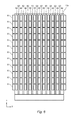
- FIG. 6 is a plan view illustrating the arrangement configuration of the touch drive electrodes 61 and the touch detection electrodes 62 .
- a plurality of touch drive electrodes 61 extending in the X axis direction are provided so as to be arrayed in the Y axis direction at predetermined intervals.
- a plurality of touch detection electrodes 62 extending in the Y axis direction are provided so as to be arrayed in the X axis direction at predetermined intervals.
- the touch drive electrodes 61 and the touch detection electrodes 62 are formed with translucent conductive films made of a material having excellent translucency and conductivity, such as indium tin oxide (ITO) or zinc oxide (ZnO).
- ITO indium tin oxide
- ZnO zinc oxide
- the touch drive electrodes 61 are sequentially scanned so that an input signal is input thereto, and output signals output from the touch detection electrodes 62 are detected.
- the electrostatic capacitance between the touch drive electrode 61 and the touch detection electrode 62 at the touched position changes. Based on an output signal output from the touch detection electrode 62 , the position where the electrostatic capacitance has changed is detected, and the detected position is identified as the touched position.
- the dummy electrodes 63 are provided between the plurality of the touch detection electrodes 62 provided on the front side of the CF substrate 11 a .
- the dummy electrodes 63 are provided in each space between adjacent ones of the plurality of touch detection electrodes 62 arrayed in the X axis direction at predetermined intervals.
- the dummy electrodes 63 are provided for the purpose of preventing the light transmission rate and the like from becoming different between the positions where the touch detection electrodes 62 are provided and the positions where they are not provided, on the front side of the CF substrate 11 a .
- the dummy electrodes 63 therefore, are formed with conductive films made of the same material as that of the touch detection electrodes 62 , that is, a material having excellent translucency, such as ITO or ZnO. It should be noted that the dummy electrodes 63 are not connected with other lines or electrodes, and are in an electrically floating state.
- the touch detection electrodes 62 and the dummy electrodes 63 have predetermined refractive indices, though they are transparent. In the touch detection electrodes 62 and the dummy electrodes 63 , therefore, a plurality of slits are provided so as to make the touch detection electrodes 62 and the dummy electrodes 63 unnoticeable when the touch sensor-equipped liquid crystal display device 10 is viewed.
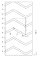
- FIG. 7 is a diagram for explaining the shape of slits provided in the touch detection electrodes 62 . It should be noted that slits in the identical shape are provided in the dummy electrodes 63 , though the illustration of the same is omitted.
- the touch detection electrode 62 is composed of a plurality of electrode portions 621 formed with translucent conductive films, and a plurality of slits 622 provided between the plurality of electrode portions 621 .
- Each slit 622 is repeatedly bent in a zigzag shape, while extending in the Y axis direction as an entire slit.
- each slit 622 is composed of first direction linear portions 622 a extending in a first direction, and second direction linear portions 622 b extending in a second direction that is different from the first direction.
- the first direction linear portions 622 a and the second direction linear portions 622 b have the same width in the X axis direction, and the same length in the Y axis direction.
- an arrangement interval “a” for the slits 622 adjacent in the X axis direction in a plan view satisfies the relationship given as the following expression (1):
- b represents an arrangement interval for a plurality of the display pixels adjacent in the X axis direction in a plan view
- ⁇ represents an angle of the slit 622 with respect to the Y axis direction as a reference direction
- the turnback width “c” of the slit 622 in the zigzag shape is set to (the distance between the centers of the subpixels adjacent in the X axis direction among the plurality of subpixels composing one display pixel) ⁇ a natural number equal to or greater than (the number of colors of the subpixels+1) ⁇ .
- the turnback width “c” of the slit 622 is a width of the first direction linear portion 622 a (or the second direction linear portion 622 b ) in the X axis direction.
- the turnback width “c” of the slit 622 is assumed to be ⁇ (the distance between the centers of the subpixels) ⁇ (a natural number equal to or greater than 4) ⁇ .
- the turnback width “c” of the slit 622 is set to ⁇ (the distance between the centers of the subpixels) ⁇ 4 ⁇ .
- the width “d” of the slit 622 in the X axis direction is 20 ⁇ m or less. Further, it is preferable that the arrangement interval “a” of the slits 622 adjacent in the X axis direction is 175 ⁇ m or less.
- the angle ⁇ of the slit 622 is preferably 25° to 45°, and is set to 30° in the present embodiment.
- FIG. 8 illustrates one exemplary arrangement of color filters 11 h.
- FIG. 9 is a diagram obtained by superposing the diagram of a configuration of the touch detection electrode 62 illustrated in FIG. 7 , on the diagram of color filter arrangement illustrated in FIG. 8 .
- FIG. 9 illustrates the arrangement interval “a” for the slits 622 , and the arrangement interval “b” for the display pixels as well.
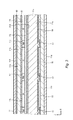
- FIGS. 10A to 10F illustrate differences in appearance of the display screen when the arrangement interval “a” for the slits 622 is varied with respect to the arrangement interval “b” for the display pixels.
- Each of FIGS. 10A to 10F is an enlarged view illustrating a part of the display screen when white color display is performed in the entire display screen.
- the arrangement interval “a” for the slits 622 is set to 1.000 time, 1.225 times, 1.250 times, 1.500 times, 1.725 times, and 2.000 times the arrangement interval “b” for the display pixels, respectively.
- FIG. 10E illustrates the appearance of the display screen when the arrangement interval “a” for the slits 622 is set so as to satisfy the expression (1) and white color display is performed in the entire display screen.
- the following also describes the appearance of the display screen in a case where the arrangement interval “a” for the slits 622 is set so as to satisfy the following expression (1), and display other than the white color display is performed.
- FIGS. 11A to 11C are enlarged views illustrating a part of the display screen in cases where the arrangement interval “a” for the slits 622 is set so as to satisfy the expression (1) and displays illustrated in FIGS. 17A to 17C are performed.
- FIG. 11A illustrates a display screen in a case where a black-and-white vertical stripe display is performed (corresponding to FIG. 12A )
- FIG. 11B illustrates a display screen in a case where a black-and-white chessboard pattern display is performed (corresponding to FIG. 12B )
- FIG. 11C illustrates a display screen in a case where an RGB chessboard pattern display is performed (corresponding to FIG. 12C ).
- the arrangement interval “a” for the slits 622 is set so as to satisfy the expression (1), clear moire is not seen, in any one of the case where the black-and-white vertical stripe display ( FIG. 11A ) is performed, the case where the black-and-white chessboard pattern display ( FIG. 11B ) is performed, and the case where the RGB chessboard pattern display ( FIG. 11C ) is performed, as is the case where white color display is performed in the entire display screen ( FIG. 10E ).
- the present invention is not limited to the above-described embodiment.
- the foregoing description refers to a liquid crystal panel as an exemplary display panel in which a display function layer including a plurality of display pixels arranged in matrix is provided between a pair of substrates, but the display panel may be another display panel such as an organic electroluminescence (EL) panel including organic EL elements.
- EL organic electroluminescence
- the colors of the subpixels are three colors of R (red), G (green), and B (blue), but the colors may be four colors of R (red), G (green), B (blue), and Y (yellow), or alternatively, five or more colors.
- the touch sensor-equipped display device in the present embodiment is used in various types of electronic devices such as mobile phones (including smartphones), notebook computers (including tablet-type notebook computers), portable information terminals (including electronic books and PDAs), digital photoframes, and portable game machines.
- mobile phones including smartphones
- notebook computers including tablet-type notebook computers
- portable information terminals including electronic books and PDAs
- digital photoframes and portable game machines.
Landscapes
- Engineering & Computer Science (AREA)
- General Engineering & Computer Science (AREA)
- Theoretical Computer Science (AREA)
- Human Computer Interaction (AREA)
- Physics & Mathematics (AREA)
- General Physics & Mathematics (AREA)
- Devices For Indicating Variable Information By Combining Individual Elements (AREA)
- Quality & Reliability (AREA)
- Liquid Crystal (AREA)
Abstract
Provided is a touch sensor-equipped display device in which moire occurring due to interference between an array pattern of subpixels and a pattern of slits in a touch detection electrode is suppressed. The touch sensor-equipped display device includes a display panel including a plurality of display pixels arranged in matrix, a touch drive electrode extending in a first direction, and a touch detection electrode extending in a second direction that intersects with the first direction at a right angle. In the touch detection electrode, a plurality of slits each of which is repeatedly bent in a zigzag shape while extending in the second direction are provided so as to be arrayed in the first direction. An arrangement interval “a” for the slits adjacent in the first direction satisfies relationship given as:
a=b×(0.725+n)×√3÷(2×cos θ)
where “b” represents an arrangement interval for the display pixels adjacent in the first direction. “θ” represents an angle of the slits with respect to the second direction as a reference direction, and “n” represents an integer equal to or greater than 0. A turnback width of the slits is set to (a distance between centers of subpixels adjacent in the first direction among subpixels composing one display pixel)×{a natural number equal to or greater than (the number of colors of the subpixels+1)}.
Description
- The present invention relates to a touch sensor-equipped display device.
-
Patent Document 1 discloses a touch sensor-equipped display device that includes touch drive electrodes and touch detection electrodes. In this touch sensor-equipped display device, slits are provided in the touch detection electrodes so that the touch detection electrodes become unnoticeable to human eye. -
- Patent Document 1: JP-A-2014-130537
- If, however, the array pattern of subpixels that compose a plurality of display pixels arranged in matrix, and the pattern of the slits in the touch detection electrodes interfere with each other, moire occurs, whereby the display quality of the display device decreases.
- It is an object of the present invention to provide a touch sensor-equipped display device in which interference between the array pattern of sub pixels that compose display pixels and the pattern of slits in the detection electrodes is suppressed.
- A touch sensor-equipped display device in one embodiment of the present invention includes: a display panel including a first substrate, a second substrate opposed to the first substrate, and a display function layer interposed between the first substrate and the second substrate, the display function layer including a plurality of display pixels arranged in matrix; a touch drive electrode that is provided between the first substrate and the second substrate and extends in a first direction; and a touch detection electrode that is provided on a surface of the first substrate on a side opposite to the touch drive electrode, and extends in a second direction that intersects with the first direction at a right angle. In the touch sensor-equipped display device, a plurality of slits each of which is repeatedly bent in a zigzag shape while extending in the second direction are provided in the touch detection electrode so as to be arrayed in the first direction; an arrangement interval “a” for the slits adjacent in the first direction satisfies relationship given as:
-
a=b×(0.725+n)×√3÷(2×cos θ) - where “b” represents an arrangement interval for the display pixels adjacent in the first direction, “θ” represents an angle of the slits with respect to the second direction as a reference direction, and “n” represents an integer equal to or greater than 0; and a turnback width of the slits in the zigzag shape is set to (a distance between centers of subpixels adjacent in the first direction among subpixels composing one display pixel)×{a natural number equal to or greater than (the number of colors of the subpixels+1)}.
- With the present invention, the occurrence of moire caused by the interference between the array pattern of subpixels and the pattern of the slits in the touch detection electrode can be suppressed, whereby the display quality of the display device can be improved.
-
FIG. 1 illustrates a cross-sectional configuration of a touch sensor-equipped display device in one embodiment. -
FIG. 2 is a plan view illustrating the touch sensor-equipped display device in one embodiment. -
FIG. 3 is a schematic cross-sectional view of a liquid crystal panel with a touch sensor function. -
FIG. 4 is an enlarged plan view illustrating a plan-view configuration in a display section of an array substrate that composes the liquid crystal panel with a touch sensor function. -
FIG. 5 is an enlarged plan view illustrating a plan-view configuration in a display section of a CF substrate that composes the liquid crystal panel with a touch sensor function. -
FIG. 6 is a plan view illustrating an arrangement configuration of touch drive electrodes and touch detection electrodes. -
FIG. 7 is a diagram for explaining a shape of a slit provided in touch detection electrodes. -
FIG. 8 illustrates one exemplary arrangement of color filters. -
FIG. 9 is a diagram obtained by superposing the diagram of the touch detection electrode configuration illustrated inFIG. 7 on the diagram of color filter arrangement illustrated inFIG. 8 . -
FIG. 10A is an enlarged view illustrating a part of the display screen when the entirety of the display screen is in a white color display state, in a case where the arrangement interval “a” for the slits is set to 1.000 time the arrangement interval “b” for the display pixels. -
FIG. 10B is an enlarged view illustrating a part of the display screen when the entirety of the display screen is in a white color display state, in a case where the arrangement interval “a” for the slits is set to 1.225 times the arrangement interval “b” for the display pixels. -
FIG. 10C is an enlarged view illustrating a part of the display screen when the entirety of the display screen is in a white color display state, in a case where the arrangement interval “a” for the slits is set to 1.250 times the arrangement interval “b” for the display pixels. -
FIG. 10D is an enlarged view illustrating a part of the display screen when the entirety of the display screen is in a white color display state, in a case where the arrangement interval “a” for the slits is set to 1.500 times the arrangement interval “b” for the display pixels. -
FIG. 10E is an enlarged view illustrating a part of the display screen when the entirety of the display screen is in a white color display state, in a case where the arrangement interval “a” for the slits is set to 1.725 times the arrangement interval “b” for the display pixels. -
FIG. 10F is an enlarged view illustrating a part of the display screen when the entirety of the display screen is in a white color display state, in a case where the arrangement interval “a” for the slits is set to 2.000 times the arrangement interval “b” for the display pixels. -
FIG. 11A is an enlarged view illustrating a part of the display screen when a black-and-white vertical stripe display is performed, in a case where the arrangement interval “a” for the slits is set to 1.725 times the arrangement interval “b” for the display pixels. -
FIG. 11B is an enlarged view illustrating a part of the display screen when a black-and-white chessboard pattern display is performed, in a case where the arrangement interval “a” for the slits is set to 1.725 times the arrangement interval “b” for the display pixels. -
FIG. 11C is an enlarged view illustrating a part of the display screen when an RCSB chessboard pattern display is performed, in a case where the arrangement interval “a” for the slits is set to 1.725 times the arrangement interval “b” for the display pixels. -
FIG. 12A is a diagram for explaining a method for displaying a black-and-white vertical stripe display. -
FIG. 12B is a diagram for explaining a black-and-white chessboard pattern display. -
FIG. 12C is a diagram for explaining a black-and-white chessboard pattern display. - A touch sensor-equipped display device in one embodiment of the present invention includes: a display panel including a first substrate, a second substrate opposed to the first substrate, arid a display function layer interposed between the first substrate and the second substrate, the display function layer including a plurality of display pixels arranged in matrix; a touch drive electrode that is provided between the first substrate and the second substrate and extends in a first direction; and a touch detection electrode that is provided on a surface of the first substrate on a side opposite to the touch drive electrode, and extends in a second direction that intersects with the first direction at a right angle. In the touch sensor-equipped display device, a plurality of slits each of which is repeatedly bent in a zigzag shape while extending in the second direction are provided in the touch detection electrode so as to be arrayed in the first direction; an arrangement interval “a” for the slits adjacent in the first direction satisfies relationship given as:
-
a=b×(0.725+n)×√3÷(2×cos θ) - where “b” represents an arrangement interval for the display pixels adjacent in the first direction, “θ” represents an angle of the slits with respect to the second direction as a reference direction, and “n” represents an integer equal to or greater than 0; and a turnback width of the slits in the zigzag shape is set to (a distance between centers of subpixels adjacent in the first direction among subpixels composing one display pixel)×{a natural number equal to or greater than (the number of colors of the subpixels +1)} (the first configuration).
- With the first configuration, the occurrence of moire caused by the interference between the array pattern of subpixels and the pattern of the slits in the touch detection electrode can be suppressed, whereby the display quality of the display device can be improved.
- In the first configuration, the slits have a width of 20 μm or less (the second configuration).
- With the second configuration, the occurrence of moire can be suppressed, whereby the display quality of the display device can be improved.
- In the first or second configuration, the arrangement interval “a” for the slits is 175 μm or less (the third configuration).
- With the third configuration, the occurrence of moire can be suppressed, whereby the display quality of the display device can be improved.
- In any one of the first to third configurations, the angle θ for the slits is in a range of 25° to 45° (the fourth configuration).
- With the fourth configuration, the occurrence of moire can be suppressed, whereby the display quality of the display device can be improved.
- The following describes embodiments of the present invention in detail, while referring to the drawings. Identical or equivalent parts in the drawings are denoted by the same reference numerals, and the descriptions of the same are not repeated. To make the description easy to understand, in the drawings referred to hereinafter, the configurations are simply illustrated or schematically illustrated, or the illustration of part of constituent members is omitted. Further, the dimension ratios of the constituent members illustrated in the drawings do not necessarily indicate the real dimension ratios.
-
FIG. 1 illustrates a cross-sectional configuration of a touch sensor-equippeddisplay device 10 in one embodiment.FIG. 2 is a plan view illustrating the touch sensor-equippeddisplay device 10 in one embodiment. The touch sensor-equippeddisplay device 10 includes aliquid crystal panel 11 with a touch sensor function, a backlight device (lighting device) 13, abezel 14, acase 15, and acover 16. Regarding this touch sensor-equippeddisplay device 10, the side thereof on which thecover 16 is provided is the front side, and the side thereof on which thecase 15 is provided is the rear side. - The
liquid crystal panel 11 with a touch sensor function has a function of displaying an image, and a touch sensor function of detecting a touched position. More specifically, theliquid crystal panel 11 with a touch sensor function has a configuration that includes: a liquid crystal panel (display panel) that includes a pair of substrates and a display function layer provided between the substrates, the display function layer including a plurality of display pixels provided in matrix; touch drive electrodes provided between the pair of substrates of the liquid crystal panel; and touch detection electrodes provided on a front side of the substrate on the front side of the display panel. - The
backlight device 13 is an external light source that emits light toward theliquid crystal panel 11 with a touch sensor function. - The
cover 16 is arranged on an outer side of theliquid crystal panel 11 with a touch sensor function so as to protect theliquid crystal panel 11 with a touch sensor function. Thiscover 16 is made of a material that has excellent impact resistance, for example, tempered glass. Theliquid crystal panel 11 with a touch sensor function, and thecover 16, are bonded and integrated with each other with an approximately transparent adhesive (not shown) being interposed therebetween. - The
bezel 14 holds thecover 16 and theliquid crystal panel 11 with a touch sensor function together, between the same and thebacklight device 13. Thebezel 14 is attached to thecase 15, and thecase 15 houses thebacklight device 13. -
FIG. 3 is a schematic cross-sectional view of theliquid crystal panel 11 with a touch sensor function.FIG. 4 is an enlarged plan view illustrating a plan-view configuration in a display section of an array substrate that composes theliquid crystal panel 11 with a touch sensor function.FIG. 5 is an enlarged plan view illustrating a plan-view configuration in a display section of a CF substrate that composes theliquid crystal panel 11 with a touch sensor function. - The
liquid crystal panel 11 with a touch sensor function includes a pair ofsubstrates liquid crystal layer 11 c interposed between thesubstrates FIG. 3 . Theliquid crystal layer 11 c contains liquid crystal molecules as a substance whose optical properties change in response to the application of an electric field. Thesubstrates liquid crystal layer 11 c is maintained therebetween. - Each of the
substrates substrates - On the inner side surfaces of the
substrates alignment films liquid crystal layer 11 c are formed, respectively, as illustrated inFIG. 3 . On the outer side surfaces of thesubstrates polarizing plates - On the inner side surface of the
array substrate 11 b (theliquid crystal layer 11 c side, the side opposed to theCF substrate 11 a), a plurality of thin film transistors (TFTs) 17, which are switching elements, and a plurality ofpixel electrodes 18, are provided in matrix, as illustrated inFIGS. 3 and 4 .Gate lines 19 andsource lines 20 forming a lattice pattern are arranged so as to enclose theseTFTs 17 andpixel electrodes 18. In other words, at intersections of the gate lines 19 and the source lines 20 forming the lattice pattern, theTFTs 17 and thepixel electrodes 18 are arranged in parallel, so as to be arranged in matrix. - The gate lines 19 and the source lines 20 are connected to the gate electrodes and the source electrodes of the
TFTs 17, respectively, and thepixel electrodes 18 are connected to the drain electrodes of theTFTs 17. Further, eachpixel electrode 18 is in a portrait oriented rectangular shape when viewed in a plan view, and is formed with a translucent conductive film made of a material having excellent translucency and conductivity, such as indium tin oxide (ITO) or zinc oxide (ZnO). - On the other hand, as illustrated in
FIGS. 3 and 5 ,color filters 11 h are provided in matrix on theCF substrate 11 a, in such a manner that the color portions in colors of red (R), green (G), blue (B) and the like overlap thepixel electrodes 18 on thearray substrate 11 b side when viewed in a plan view. Between the respective color portions that form thecolor filter 11 h, a light-shielding layer (black matrix) 11 i in a lattice pattern for preventing the color mixing is formed. The light-shielding layer 11 i is arranged so as to overlap the above-describedgate lines 19 and the source lines 20 when viewed in a plan view. Over an entire surface of thecolor filters 11 h and the light-shielding layer 11 i, a counter electrode 11 j is provided, which is opposed to thepixel electrodes 18 on thearray substrate 11 b side. - In this
liquid crystal panel 11 with a touch sensor function, as illustrated inFIGS. 3 to 5 , one display pixel as a display unit is composed of a set of the color portions in the three colors of R (red), G (green), and B (blue) and the threepixel electrodes 18 opposed to the color portions, respectively. The display pixel is composed of a red color subpixel having a color portion of R, a green color subpixel having a color portion of G, and a blue color subpixel having a color portion of B. These subpixels of the respective colors are arranged side by side repeatedly in the row direction (X axis direction) on the plate surface of theliquid crystal panel 11, thereby forming a pixel group, and a multiplicity of such pixel groups are arrayed in the column direction (Y axis direction). In other words, a plurality of the display pixels are arranged in matrix. In the present embodiment, the subpixels are arranged in a so-called stripe array. - The following describes the touch sensor function. The
liquid crystal panel 11 with a touch sensor function includestouch drive electrodes 61 andtouch detection electrodes 62 that compose the touch sensor. As illustrated inFIG. 3 , thetouch drive electrodes 61 are provided on the back side (theliquid crystal layer 11 c side) of theCF substrate 11 a, and thetouch detection electrodes 62 are provided on the front side of theCF substrate 11 a. More specifically, thetouch drive electrodes 61 are provided between theCF substrate 11 a on one hand and thecolor filters 11 h and the light-shielding layer 11 i on the other hand. Further, thetouch detection electrodes 62 are provided between theCF substrate 11 a and thepolarizing plate 11 f. This touch sensor is of the so-called projection type electrostatic capacitance method, and the detection method thereof is of the mutual capacitance type. -
FIG. 6 is a plan view illustrating the arrangement configuration of thetouch drive electrodes 61 and thetouch detection electrodes 62. A plurality oftouch drive electrodes 61 extending in the X axis direction are provided so as to be arrayed in the Y axis direction at predetermined intervals. Further, a plurality oftouch detection electrodes 62 extending in the Y axis direction are provided so as to be arrayed in the X axis direction at predetermined intervals. Thetouch drive electrodes 61 and thetouch detection electrodes 62 are formed with translucent conductive films made of a material having excellent translucency and conductivity, such as indium tin oxide (ITO) or zinc oxide (ZnO). - The following simply explains a method for detecting a touched position. The
touch drive electrodes 61 are sequentially scanned so that an input signal is input thereto, and output signals output from thetouch detection electrodes 62 are detected. When any area of the surface of the touch sensor-equippeddisplay device 10 is touched, the electrostatic capacitance between thetouch drive electrode 61 and thetouch detection electrode 62 at the touched position changes. Based on an output signal output from thetouch detection electrode 62, the position where the electrostatic capacitance has changed is detected, and the detected position is identified as the touched position. - Between the plurality of the
touch detection electrodes 62 provided on the front side of theCF substrate 11 a, thedummy electrodes 63 are provided. In other words, in each space between adjacent ones of the plurality oftouch detection electrodes 62 arrayed in the X axis direction at predetermined intervals, a plurality ofdummy electrodes 63 extending in the Y axis direction are provided. - The
dummy electrodes 63 are provided for the purpose of preventing the light transmission rate and the like from becoming different between the positions where thetouch detection electrodes 62 are provided and the positions where they are not provided, on the front side of theCF substrate 11 a. Thedummy electrodes 63, therefore, are formed with conductive films made of the same material as that of thetouch detection electrodes 62, that is, a material having excellent translucency, such as ITO or ZnO. It should be noted that thedummy electrodes 63 are not connected with other lines or electrodes, and are in an electrically floating state. - The
touch detection electrodes 62 and thedummy electrodes 63 have predetermined refractive indices, though they are transparent. In thetouch detection electrodes 62 and thedummy electrodes 63, therefore, a plurality of slits are provided so as to make thetouch detection electrodes 62 and thedummy electrodes 63 unnoticeable when the touch sensor-equipped liquidcrystal display device 10 is viewed. -
FIG. 7 is a diagram for explaining the shape of slits provided in thetouch detection electrodes 62. It should be noted that slits in the identical shape are provided in thedummy electrodes 63, though the illustration of the same is omitted. - The
touch detection electrode 62 is composed of a plurality ofelectrode portions 621 formed with translucent conductive films, and a plurality ofslits 622 provided between the plurality ofelectrode portions 621. Eachslit 622 is repeatedly bent in a zigzag shape, while extending in the Y axis direction as an entire slit. In other words, each slit 622 is composed of first directionlinear portions 622 a extending in a first direction, and second directionlinear portions 622 b extending in a second direction that is different from the first direction. Here, the first directionlinear portions 622 a and the second directionlinear portions 622 b have the same width in the X axis direction, and the same length in the Y axis direction. - In the present embodiment, an arrangement interval “a” for the
slits 622 adjacent in the X axis direction in a plan view satisfies the relationship given as the following expression (1): -
a=b×(0.725+n)×√3÷(2×cos θ) (1) - where “b” represents an arrangement interval for a plurality of the display pixels adjacent in the X axis direction in a plan view, “θ” represents an angle of the
slit 622 with respect to the Y axis direction as a reference direction, and “n” represents an integer equal to or greater than 0 (n=0, 1, 2, . . . ). - Further, the turnback width “c” of the
slit 622 in the zigzag shape is set to (the distance between the centers of the subpixels adjacent in the X axis direction among the plurality of subpixels composing one display pixel)×{a natural number equal to or greater than (the number of colors of the subpixels+1)}. The turnback width “c” of theslit 622 is a width of the first directionlinear portion 622 a (or the second directionlinear portion 622 b) in the X axis direction. For example, in a case where the subpixels correspond to the three colors of R (red), G (green), and B (blue), the turnback width “c” of theslit 622 is assumed to be {(the distance between the centers of the subpixels)×(a natural number equal to or greater than 4)}. In the present embodiment, the turnback width “c” of theslit 622 is set to {(the distance between the centers of the subpixels)×4}. - It is preferable that the width “d” of the
slit 622 in the X axis direction is 20 μm or less. Further, it is preferable that the arrangement interval “a” of theslits 622 adjacent in the X axis direction is 175 μm or less. - The angle θ of the
slit 622 is preferably 25° to 45°, and is set to 30° in the present embodiment. -
FIG. 8 illustrates one exemplary arrangement ofcolor filters 11 h. Further,FIG. 9 is a diagram obtained by superposing the diagram of a configuration of thetouch detection electrode 62 illustrated inFIG. 7 , on the diagram of color filter arrangement illustrated inFIG. 8 .FIG. 9 illustrates the arrangement interval “a” for theslits 622, and the arrangement interval “b” for the display pixels as well. It should be noted that the arrangement interval “a” for theslits 622 is the arrangement interval in a case where n=1 and θ=30° in the expression (1), that is, 1.725 times the arrangement interval “b” for the display pixels. -
FIGS. 10A to 10F illustrate differences in appearance of the display screen when the arrangement interval “a” for theslits 622 is varied with respect to the arrangement interval “b” for the display pixels. Each ofFIGS. 10A to 10F is an enlarged view illustrating a part of the display screen when white color display is performed in the entire display screen. InFIGS. 10A to 10F , the arrangement interval “a” for theslits 622 is set to 1.000 time, 1.225 times, 1.250 times, 1.500 times, 1.725 times, and 2.000 times the arrangement interval “b” for the display pixels, respectively. - In the case where the arrangement interval “a” for the
slits 622 is set to 1.000 time the arrangement interval “b” for the display pixels, wide horizontal lines are visible as moire, as illustrated inFIG. 10A . In the case where the arrangement interval “a” for theslits 622 is set to 1.225 times or 1.250 times the arrangement interval “b” for the display pixels, thin diagonal lines are visible as moire, as illustrated inFIG. 10B orFIG. 10C . In the case where the arrangement interval “a” for theslits 622 is set to 1.500 times or 2.000 times the arrangement interval “b” for the display pixels, wide horizontal lines are visible as moire, as illustrated inFIG. 10D orFIG. 10F . - On the other hand, in the case where the arrangement interval “a” for the
slits 622 is set to 1.725 times the arrangement interval “b” for the display pixels so as to satisfy the relationship given as the expression (1), clear moire is not seen as illustrated inFIG. 10E . -
FIG. 10E illustrates the appearance of the display screen when the arrangement interval “a” for theslits 622 is set so as to satisfy the expression (1) and white color display is performed in the entire display screen. The following also describes the appearance of the display screen in a case where the arrangement interval “a” for theslits 622 is set so as to satisfy the following expression (1), and display other than the white color display is performed. -
FIGS. 11A to 11C are enlarged views illustrating a part of the display screen in cases where the arrangement interval “a” for theslits 622 is set so as to satisfy the expression (1) and displays illustrated inFIGS. 17A to 17C are performed. Here, also, the arrangement interval “a” for theslits 622 is set to the interval in the case where n=1 and θ=30° in the expression (1), that is, set to 1.725 times the arrangement interval “b” for the display pixels. -
FIG. 11A illustrates a display screen in a case where a black-and-white vertical stripe display is performed (corresponding toFIG. 12A ),FIG. 11B illustrates a display screen in a case where a black-and-white chessboard pattern display is performed (corresponding toFIG. 12B ), andFIG. 11C illustrates a display screen in a case where an RGB chessboard pattern display is performed (corresponding toFIG. 12C ). In a case where the arrangement interval “a” for theslits 622 is set so as to satisfy the expression (1), clear moire is not seen, in any one of the case where the black-and-white vertical stripe display (FIG. 11A ) is performed, the case where the black-and-white chessboard pattern display (FIG. 11B ) is performed, and the case where the RGB chessboard pattern display (FIG. 11C ) is performed, as is the case where white color display is performed in the entire display screen (FIG. 10E ). - The present invention is not limited to the above-described embodiment. For example, the foregoing description refers to a liquid crystal panel as an exemplary display panel in which a display function layer including a plurality of display pixels arranged in matrix is provided between a pair of substrates, but the display panel may be another display panel such as an organic electroluminescence (EL) panel including organic EL elements.
-
a=b×(0.725+n)×√3÷(2×cos θ) - In the foregoing description, the colors of the subpixels are three colors of R (red), G (green), and B (blue), but the colors may be four colors of R (red), G (green), B (blue), and Y (yellow), or alternatively, five or more colors.
- The touch sensor-equipped display device in the present embodiment is used in various types of electronic devices such as mobile phones (including smartphones), notebook computers (including tablet-type notebook computers), portable information terminals (including electronic books and PDAs), digital photoframes, and portable game machines.
-
- 10 . . . touch sensor-equipped display device
- 11 . . . touch sensor-equipped liquid crystal panel
- 11 a . . . CF substrate
- 11 b . . . array substrate
- 61 . . . touch drive electrode
- 62 . . . touch detection electrode
- 622 . . . slit
Claims (4)
1. A touch sensor-equipped display device comprising:
a display panel that includes:
a first substrate;
a second substrate opposed to the first substrate; and
a display function layer interposed between the first substrate and the second substrate, the display function layer including a plurality of display pixels arranged in matrix;
a touch drive electrode that is provided between the first substrate and the second substrate and extends in a first direction; and
a touch detection electrode that is provided on a surface of the first substrate on a side opposite to the touch drive electrode, and extends in a second direction that intersects with the first direction at a right angle,
wherein a plurality of slits each of which is repeatedly bent in a zigzag shape while extending in the second direction are provided in the touch detection electrode so as to be arrayed in the first direction,
an arrangement interval “a” for the slits adjacent the first direction satisfies relationship given as:
a=b×(0.725+n)×√3÷(2×cos θ)
a=b×(0.725+n)×√3÷(2×cos θ)
where “b” represents an arrangement interval for the display pixels adjacent in the first direction, “θ” represents an angle of the slits with respect to the second direction as a reference direction, and “n” represents an integer equal to or greater than 0, and
a turnback width of the slits in the zigzag shape is set to (a distance between centers of subpixels adjacent in the first direction among subpixels composing one display pixel)×{a natural number equal to or greater than (the number of colors of the subpixels+1)}.
2. The touch sensor-equipped display device according to claim 1 ,
wherein the slits have a width of 20 μm or less.
3. The touch sensor-equipped display device according to claim 1 ,
wherein the arrangement interval “a” for the slits is 175 μm or less.
4. The touch sensor-equipped display device according to claim 1 ,
wherein the angle θ for the slits is in a range of 25° to 45°.
Applications Claiming Priority (3)
| Application Number | Priority Date | Filing Date | Title |
|---|---|---|---|
| JP2015-033442 | 2015-02-24 | ||
| JP2015033442 | 2015-02-24 | ||
| PCT/JP2016/055044 WO2016136662A1 (en) | 2015-02-24 | 2016-02-22 | Display device with touch sensor |
Publications (1)
| Publication Number | Publication Date |
|---|---|
| US20180046292A1 true US20180046292A1 (en) | 2018-02-15 |
Family
ID=56788393
Family Applications (1)
| Application Number | Title | Priority Date | Filing Date |
|---|---|---|---|
| US15/553,569 Abandoned US20180046292A1 (en) | 2015-02-24 | 2016-02-22 | Touch sensor-equipped display device |
Country Status (4)
| Country | Link |
|---|---|
| US (1) | US20180046292A1 (en) |
| JP (1) | JP6409117B2 (en) |
| CN (1) | CN107250961A (en) |
| WO (1) | WO2016136662A1 (en) |
Cited By (2)
| Publication number | Priority date | Publication date | Assignee | Title |
|---|---|---|---|---|
| US11182003B2 (en) * | 2017-04-14 | 2021-11-23 | Samsung Display Co., Ltd. | Touch sensor with high sensitivity and display device having the same |
| US12200887B2 (en) | 2021-10-05 | 2025-01-14 | Samsung Electronics Co., Ltd. | Electronic device including flexible display |
Families Citing this family (2)
| Publication number | Priority date | Publication date | Assignee | Title |
|---|---|---|---|---|
| KR102494560B1 (en) | 2014-12-02 | 2023-01-31 | 인벤티오 아게 | Method for providing a visitor controlled access into a building |
| CN109426399B (en) * | 2017-09-05 | 2022-03-01 | 瀚宇彩晶股份有限公司 | Touch control display device |
Citations (1)
| Publication number | Priority date | Publication date | Assignee | Title |
|---|---|---|---|---|
| US20140184560A1 (en) * | 2012-12-28 | 2014-07-03 | Japan Display Inc. | Display device with touch detection function and electronic apparatus |
Family Cites Families (5)
| Publication number | Priority date | Publication date | Assignee | Title |
|---|---|---|---|---|
| JP5812895B2 (en) * | 2012-02-28 | 2015-11-17 | 株式会社ジャパンディスプレイ | Proximity detection device, proximity detection method, electronic device |
| JP5914403B2 (en) * | 2013-03-29 | 2016-05-11 | 株式会社ジャパンディスプレイ | Display device with touch detection function and electronic device |
| JP6081881B2 (en) * | 2013-07-22 | 2017-02-15 | 日本写真印刷株式会社 | Touch panel |
| TW201530398A (en) * | 2014-01-17 | 2015-08-01 | Wintek Corp | Touch panel and touch display device |
| CN104035621B (en) * | 2014-06-24 | 2017-12-05 | 昆山龙腾光电有限公司 | Touch control display apparatus and preparation method thereof |
-
2016
- 2016-02-22 CN CN201680011346.9A patent/CN107250961A/en active Pending
- 2016-02-22 JP JP2017502348A patent/JP6409117B2/en active Active
- 2016-02-22 US US15/553,569 patent/US20180046292A1/en not_active Abandoned
- 2016-02-22 WO PCT/JP2016/055044 patent/WO2016136662A1/en not_active Ceased
Patent Citations (1)
| Publication number | Priority date | Publication date | Assignee | Title |
|---|---|---|---|---|
| US20140184560A1 (en) * | 2012-12-28 | 2014-07-03 | Japan Display Inc. | Display device with touch detection function and electronic apparatus |
Cited By (2)
| Publication number | Priority date | Publication date | Assignee | Title |
|---|---|---|---|---|
| US11182003B2 (en) * | 2017-04-14 | 2021-11-23 | Samsung Display Co., Ltd. | Touch sensor with high sensitivity and display device having the same |
| US12200887B2 (en) | 2021-10-05 | 2025-01-14 | Samsung Electronics Co., Ltd. | Electronic device including flexible display |
Also Published As
| Publication number | Publication date |
|---|---|
| JPWO2016136662A1 (en) | 2017-11-24 |
| WO2016136662A1 (en) | 2016-09-01 |
| JP6409117B2 (en) | 2018-10-17 |
| CN107250961A (en) | 2017-10-13 |
Similar Documents
| Publication | Publication Date | Title |
|---|---|---|
| US20180120986A1 (en) | Touch sensor-equipped display device | |
| CN104516153B (en) | Liquid crystal display device with a light guide plate | |
| US10175834B2 (en) | Position input device and display device | |
| TWI629623B (en) | Display device | |
| TWI564758B (en) | Display panel with touch detector, touch panel, and electronic unit | |
| CN105116637B (en) | Display panel and curved surface display | |
| US10261617B2 (en) | In-cell touch panel and display device | |
| US10379689B2 (en) | Touch panel including an insulating substrate and display device for the same | |
| CN103984158B (en) | Display panel | |
| CN104965338A (en) | Display panel and display device | |
| US10559270B2 (en) | Array substrate and display panel | |
| WO2016107098A1 (en) | Touch substrate and touch device | |
| CN104678629B (en) | Display panel | |
| CN110716336B (en) | Display device | |
| CN104216181A (en) | Display panel and curved surface display | |
| WO2016084728A1 (en) | Position input device and display device fitted with position input function | |
| US20180046292A1 (en) | Touch sensor-equipped display device | |
| US9274664B2 (en) | Display device with touch panel | |
| JP5659294B2 (en) | Display device | |
| CN115390317B (en) | Display device | |
| US9459486B2 (en) | Liquid crystal display device in which display of off state reflected light is suppressed | |
| CN103487980A (en) | Display device | |
| CN204302619U (en) | Touch display panel and electronic equipment | |
| US20160216815A1 (en) | Touch display | |
| WO2016199691A1 (en) | Position input device, and display device having position input function |
Legal Events
| Date | Code | Title | Description |
|---|---|---|---|
| AS | Assignment |
Owner name: SHARP KABUSHIKI KAISHA, JAPAN Free format text: ASSIGNMENT OF ASSIGNORS INTEREST;ASSIGNORS:MIYAZAKI, SHINICHI;KIRA, TAKATOSHI;REEL/FRAME:043673/0859 Effective date: 20170808 |
|
| STCB | Information on status: application discontinuation |
Free format text: ABANDONED -- FAILURE TO RESPOND TO AN OFFICE ACTION |