US20140192262A1 - Video demodulation device - Google Patents
Video demodulation device Download PDFInfo
- Publication number
- US20140192262A1 US20140192262A1 US14/206,833 US201414206833A US2014192262A1 US 20140192262 A1 US20140192262 A1 US 20140192262A1 US 201414206833 A US201414206833 A US 201414206833A US 2014192262 A1 US2014192262 A1 US 2014192262A1
- Authority
- US
- United States
- Prior art keywords
- signal
- cvbs
- reference value
- analog
- video
- Prior art date
- Legal status (The legal status is an assumption and is not a legal conclusion. Google has not performed a legal analysis and makes no representation as to the accuracy of the status listed.)
- Granted
Links
Images


Classifications
-
- H—ELECTRICITY
- H04—ELECTRIC COMMUNICATION TECHNIQUE
- H04N—PICTORIAL COMMUNICATION, e.g. TELEVISION
- H04N5/00—Details of television systems
- H04N5/14—Picture signal circuitry for video frequency region
- H04N5/21—Circuitry for suppressing or minimising disturbance, e.g. moiré or halo
- H04N5/213—Circuitry for suppressing or minimising impulsive noise
-
- H—ELECTRICITY
- H04—ELECTRIC COMMUNICATION TECHNIQUE
- H04N—PICTORIAL COMMUNICATION, e.g. TELEVISION
- H04N5/00—Details of television systems
- H04N5/04—Synchronising
- H04N5/08—Separation of synchronising signals from picture signals
-
- H—ELECTRICITY
- H04—ELECTRIC COMMUNICATION TECHNIQUE
- H04N—PICTORIAL COMMUNICATION, e.g. TELEVISION
- H04N5/00—Details of television systems
- H04N5/44—Receiver circuitry for the reception of television signals according to analogue transmission standards
- H04N5/455—Demodulation-circuits
-
- H—ELECTRICITY
- H04—ELECTRIC COMMUNICATION TECHNIQUE
- H04N—PICTORIAL COMMUNICATION, e.g. TELEVISION
- H04N5/00—Details of television systems
- H04N5/44—Receiver circuitry for the reception of television signals according to analogue transmission standards
- H04N5/52—Automatic gain control
-
- H—ELECTRICITY
- H04—ELECTRIC COMMUNICATION TECHNIQUE
- H04N—PICTORIAL COMMUNICATION, e.g. TELEVISION
- H04N5/00—Details of television systems
- H04N5/44—Receiver circuitry for the reception of television signals according to analogue transmission standards
- H04N5/57—Control of contrast or brightness
-
- H—ELECTRICITY
- H04—ELECTRIC COMMUNICATION TECHNIQUE
- H04N—PICTORIAL COMMUNICATION, e.g. TELEVISION
- H04N9/00—Details of colour television systems
- H04N9/64—Circuits for processing colour signals
- H04N9/66—Circuits for processing colour signals for synchronous demodulators
-
- H—ELECTRICITY
- H04—ELECTRIC COMMUNICATION TECHNIQUE
- H04N—PICTORIAL COMMUNICATION, e.g. TELEVISION
- H04N9/00—Details of colour television systems
- H04N9/77—Circuits for processing the brightness signal and the chrominance signal relative to each other, e.g. adjusting the phase of the brightness signal relative to the colour signal, correcting differential gain or differential phase
- H04N9/78—Circuits for processing the brightness signal and the chrominance signal relative to each other, e.g. adjusting the phase of the brightness signal relative to the colour signal, correcting differential gain or differential phase for separating the brightness signal or the chrominance signal from the colour television signal, e.g. using comb filter
Definitions
- the present disclosure relates to video demodulation devices which have a function of demodulating or reproducing a composite video, blanking, and sync signal (a CVBS signal) by digital processing, and which, in particular, are capable of outputting the CVBS signal. More specifically, the present disclosure relates to a technique for preventing lateral blurring of video reproduced from a CVBS signal by achieving stable horizontal synchronization by reducing a noise component included in a horizontal synchronizing signal of the CVBS signal reproduced through demodulation processing in analog telecasting.
- a pedestal voltage of the input CVBS signal is measured, and a basic voltage of a horizontal synchronizing signal is calculated by subtracting a predetermined value from the measured pedestal voltage. Only during a signaling period of the horizontal synchronizing signal, the basic voltage substituting for the CVBS signal is output, thereby removing a noise component from the horizontal synchronizing signal.
- Japanese Unexamined Patent Publication No. 2006-180501 describes a technique related to a video processing device to which a demodulated or reproduced CVBS signal is input. According to this technique, when horizontal synchronization is detected, the input CVBS signal is subjected to noise removal with use of a filter and sliced at a predetermined value, thereby preventing out-of-horizontal-synchronization even when interference occurs.
- the voltage of the horizontal synchronizing signal is replaced with the voltage calculated by subtracting the predetermined value from the pedestal voltage.
- this method has the following disadvantages. If the pedestal voltage is incorrect, the voltage of the horizontal synchronizing signal is also replaced with an incorrect voltage. Further, if the position of the horizontal synchronizing signal is incorrectly determined, the replacement of the voltage of the horizontal synchronizing signal takes place within a video period for example, and the information of video to be displayed is destroyed. In addition, it is more likely that the value of the pedestal voltage and the position of the horizontal synchronizing signal are incorrectly determined when interference occurs. Accordingly, when reproducing a CBVS signal with interference, this method adversely causes degradation of the quality of the CVBS signal.
- the noise component is removed from the input CVBS signal including the horizontal synchronizing signal by means of the filter, and thereby reducing occurrence of out-of-horizontal-synchronization even when interference occurs.
- the configuration as described in this patent document must include clamp circuits (i.e., circuits for adjusting a DC component) provided upstream and downstream of an analog-to-digital converter.
- the DC component adjustment performed by the clamp circuits is considerably affected by a noise component included in a horizontal synchronizing signal. Accordingly, the noise component disadvantageously destabilizes the DC component of the CVBS signal to be input, thereby making it difficult to achieve stable horizontal synchronization.
- a video demodulation device configured to demodulate an RF signal resulting from analog modulation of a composite video, blanking, and sync signal (a CVBS signal) including a horizontal synchronizing signal and to reproduce the CVBS signal by digital processing includes: a tuner configured to receive as input the RF signal resulting from analog modulation, and to output an analog IF signal; and a demodulator configured to receive as input the analog IF signal, and to demodulate the CVBS signal, wherein the demodulator includes an analog-to-digital converter configured to convert the analog IF signal into a digital IF signal, a luminance gain adjuster configured to perform gain adjustment of a luminance component included in the digital IF signal such that a maximum of the luminance component found within a predetermined period becomes equal to a predetermined reference value, and a synchronization corrector configured to receive as input a result of the gain adjustment, to correct a signal corresponding to a signaling period of the horizontal synchron
- a video demodulation device configured to demodulate an RF signal resulting from analog modulation of a composite video, blanking, and sync signal (a CVBS signal) including a horizontal synchronizing signal and to reproduce the CVBS signal by digital processing includes: a tuner configured to receive as input the RF signal resulting from analog modulation, and to output an analog IF signal; a demodulator configured to receive as input the analog IF signal, and to demodulate the CVBS signal, and a video processor configured to receive as input the demodulated CVBS signal, and to output a video signal by performing required processing, wherein the demodulator includes an analog-to-digital converter configured to convert the analog IF signal into a digital IF signal, an automatic phase controller configured to control and set a phase offset of a luminance component of the CVBS signal included in the digital IF signal to 0, and to output the digital IF signal as an audio/video signal, a filter configured to separate the audio/video signal into the luminance component, a
- the present disclosure it is possible to achieve, with a simple circuit, a video demodulation device which can accurately correct a horizontal synchronizing signal and reduce fluctuations of a DC component of a clamp circuit even under inferior signal-receiving conditions in which a position of horizontal synchronization is unclear.
- the video demodulation device that reduces lateral blurring of video even under inferior signal-receiving conditions can be produced at low costs.
- the present disclosure can provide highly accurate demodulation at low costs.
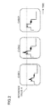
- FIG. 1 is a block diagram illustrating a configuration of a video demodulation device according to a first embodiment of the present disclosure.
- FIG. 2 is a timing chart showing operation by the luminance gain adjuster and the synchronization corrector of FIG. 1 .
- FIG. 3 is a block diagram illustrating in detail a configuration example of the luminance gain adjuster of FIG. 1 .
- FIG. 4 is a timing chart showing operation by the luminance gain adjuster of FIG. 3 .
- FIG. 5 is a block diagram illustrating in detail a configuration example of the synchronization corrector of FIG. 1
- FIG. 6 is a timing chart showing operation by the synchronization corrector of FIG. 5 .
- FIG. 7 is a timing chart showing another operation by the luminance gain adjuster and the synchronization corrector of FIG. 1 .
- FIG. 8 is a block diagram illustrating in detail a configuration example of a synchronization corrector of a video demodulation device according to a second embodiment of the present disclosure.
- FIG. 9 is a timing chart showing operation by the synchronization corrector of FIG. 8 .
- FIG. 10 is a block diagram illustrating in detail a configuration example of a synchronization corrector of a video demodulation device according to a third embodiment of the present disclosure.
- FIG. 11 is a timing chart showing operation by the synchronization corrector of FIG. 10 .
- FIG. 12A shows an image example according to a conventional technique and with severe lateral blurring
- FIG. 12B shows an image example according to the present disclosure and with reduced lateral blurring.
- FIG. 1 illustrates a configuration of a video demodulation device according to a first embodiment of the present disclosure.
- the video demodulation device 10 of FIG. 1 includes a tuner 11 , a demodulator 12 , and a video processor 13 .
- the demodulator 12 includes an analog-to-digital converter (ADC) 21 , an automatic phase controller (APC) 22 , a filter 23 , a luminance gain adjuster 24 , a synchronization corrector 25 , a clamp circuit 26 , and a digital-to-analog converter (DAC) 27 .
- ADC analog-to-digital converter
- API automatic phase controller
- the tuner 11 receives as input an RF signal resulting from analog modulation, such as negative modulation according to National Television System Committee (NTSC), of a CVBS signal, and down-converts the RF signal to output an analog IF signal.
- the demodulator 12 receives as input the analog IF signal, performs demodulation of the CVBS signal, and outputs the demodulated CVBS signal.
- the video processor 13 receives as input the CVBS signal, and performs Y/C separation and matrix processing to output a video signal.
- FIG. 2 shows operation by the luminance gain adjuster 24 and the synchronization corrector 25 of FIG. 1 .
- FIG. 2 schematically shows a flow of the signal processing from input to the luminance gain adjuster 24 to output from the synchronization corrector 25 in the demodulator 12 .
- the ADC 21 converts the input analog IF signal into a digital IF signal, and outputs the digital IF signal.
- the APC 22 receives as input the digital IF signal, controls and sets a phase offset of a luminance component of the CVBS signal included in the digital IF signal to 0, and then, outputs the digital IF signal as an audio/video signal.
- the filter 23 separates the audio/video signal into the luminance component, a color component, and an audio component, and outputs the luminance component and the color component as a first CVBS signal (CVBS 1 ). That is, the first CVBS signal (CVBS 1 ) is a composite signal including the luminance and color components.
- the luminance gain adjuster 24 performs gain adjustment of the first CVBS signal (CVBS 1 ) such that a maximum of the luminance component of the first CVBS signal (CVBS 1 ) becomes equal to a predetermined reference value A, and then, outputs the first CVBS signal as a second CVBS signal (CVBS 2 ).
- the synchronization corrector 25 receives as input the second CVBS signal (CVBS 2 ), corrects a signal corresponding to a signaling period of a horizontal synchronizing signal, and then, outputs the second CVBS signal as a third CVBS signal (CVBS 3 ).
- the clamp circuit 26 performs polarity inversion of the third CVBS signal (CVBS 3 ) input thereto, adjusts the third CVBS signal (CVBS 3 ) so as to be at a predetermined DC level, and outputs the third CVBS signal as the CVBS signal.
- the DAC 27 converts the CVBS signal into an analog signal and outputs the analog signal.
- FIG. 3 illustrates in detail a configuration example of the luminance gain adjuster 24 of FIG. 1
- FIG. 4 shows operation by the luminance gain adjuster 24 of FIG. 3
- the luminance gain adjuster 24 includes a multiplier 241 , a V-filter 242 , a peak detector 243 , a difference detector 244 , and a cumulative adder 245 .
- the multiplier 241 of the luminance gain adjuster 24 receives as input the first CVBS signal and a gain value, and outputs the product of multiplying the first CVBS signal by the gain value as the second CVBS signal (CVBS 2 ).
- the V-filter 242 which is made of a filter having a pass-band of about 300 kHz removes the color component and a noise component from the second CVBS signal (CVBS 2 ), and outputs the luminance component.
- the peak detector 243 detects the maximum of the input luminance component within a cycle of the horizontal synchronizing signal, renews the maximum in every cycle, and outputs the renewed maximum as a peak value.
- the difference detector 244 calculates a difference between the peak value and the reference value A which can be set as desired, and outputs the difference as difference information.
- the cumulative adder 245 performs smoothing by adding to an accumulated value the quotient of the difference information divided by a which is a constant, and outputs the smoothed value as the gain value to the multiplier 241 .
- the initial value of the accumulated value is set to 1.000, for example.
- the gain value converges to a value at which the reference value A and the peak value become equal to each other.
- FIG. 5 illustrates in detail a configuration example of the synchronization corrector 25 of FIG. 1
- FIG. 6 shows operation by the synchronization corrector 25 of FIG. 5
- the synchronization corrector 25 includes a comparator 251 and a selector 252 .
- the comparator 251 of the synchronization corrector 25 receives, as input, the second CVBS signal (CVBS 2 ) and the reference value A.
- the comparator 251 of the synchronization corrector 25 outputs, as a comparison signal, 1 when the second CVBS signal (CVBS 2 ) is equal to or greater than the reference value A, or 0 when the second CVBS signal (CVBS 2 ) is smaller than the reference value A.
- the selector 252 outputs, as the third CVBS signal (CVBS 3 ), the reference value A when the comparison signal is 1, or the second CVBS signal (CVBS 2 ) when the comparison signal is 0.
- the luminance gain adjuster 24 outputs the second CVBS signal (CVBS 2 ) after performing gain adjustment of the first CVBS signal (CVBS 1 ) such that the maximum of the luminance component of the second CVBS signal (CVBS 2 ) becomes equal to the reference value A. Accordingly, letting (1) be the maximum of the luminance component of CVBS 2 , and letting (2) be the reference value A, (1) is equal to (2).
- a noise component is the only signal that is greater than a horizontal synchronizing signal at this processing stage, and the horizontal synchronizing signal includes the luminance component only. Accordingly, letting (1) be the maximum of the luminance component of CVBS 2 , and letting (3) be the value of the horizontal synchronizing signal of CVBS 2 , (1) is equal to (3). Thus, (2) is also equal to (3).
- the noise component can be effectively removed from the horizontal synchronizing signal.
- the luminance gain adjuster 24 operates such that the maximum of the luminance component of the second CVBS signal (CVBS 2 ) is constantly equal to the reference value A, almost no error exists between the magnitude which the horizontal synchronizing signal of the second CVBS signal (CVBS 2 ) is supposed to have and the reference value A. Therefore, even when a low-quality signal is received, it is possible to achieve stable horizontal synchronization while reducing lateral blurring of video by accurately correcting the horizontal synchronizing signal.
- the present disclosure is not limited to the video demodulation device 10 that receives with an antenna the RF analog-modulated signal by negative modulation.
- the synchronization corrector 25 and the luminance gain adjuster 24 do not necessarily have to use the exactly same reference value A, and the reference value A may be adjusted according to increase or decrease in a preset value, as illustrated in FIG. 7 . In this manner, it is possible to change the intensity of noise component removal.
- the V-filter 242 has a pass-band of 300 kHz, for example. Note that the present disclosure is not limited to the values described above.
- a video demodulation device is configured and operates in the same manner as the video demodulation device 10 of the first embodiment, except the synchronization corrector 25 included in the demodulator 12 .
- FIG. 8 illustrates in detail a configuration example of the synchronization corrector 25 included in the video demodulation device 10 according to the second embodiment of the present disclosure
- FIG. 9 shows operation by the synchronization corrector 25 of FIG. 8
- reference numeral 253 denotes a synchronization detector
- reference numeral 254 denotes a controller.
- the comparator 251 of the synchronization corrector 25 receives, as input, a second CVBS signal (CVBS 2 ) and a reference value A.
- the comparator 251 outputs, as a comparison signal, 1 when the second CVBS signal (CVBS 2 ) is equal to or greater than the reference value A, or 0 when the second CVBS signal (CVBS 2 ) is smaller than the reference value A.
- the selector 252 outputs, as a corrected second CVBS signal (CVBS 2 ′), the reference value A when the comparison signal is 1, or the second CVBS signal (CVBS 2 ) as it is when the comparison signal is 0.
- the synchronization detector 253 outputs, as a horizontal synchronizing pulse, 1 during the signaling period of the horizontal synchronizing signal of the second CVBS signal (CVBS 2 ), or 0 during periods except the signaling period.
- the controller 254 outputs, as the third CVBS signal (CVBS 3 ), the corrected second CVBS signal (CVBS 2 ′) when the horizontal synchronizing pulse is 1 , or the second CVBS signal (CVBS 2 ) when the horizontal synchronizing pulse is 0.
- the controller 254 may output, as the third CVBS signal (CVBS 3 ), the reference value A when the horizontal synchronizing pulse is 1 , or the second CVBS signal (CVBS 2 ) when the horizontal synchronizing pulse is 0.
- the horizontal synchronizing pulse is output from the synchronization detector 253 .
- another horizontal synchronizing pulse which occurs in other block such as the video processor 13 and of which delay is adjusted may be used.
- a video demodulation device is configured and operates in the same manner as the video demodulation device 10 of the first embodiment, except the synchronization corrector 25 included in the demodulator 12 .
- FIG. 10 illustrates in detail a configuration example of the synchronization corrector 25 included in the video demodulation device 10 according to the third embodiment of the present disclosure
- FIG. 11 shows operation by the synchronization corrector 25 of FIG. 10
- reference numeral 253 denotes the synchronization detector
- reference numeral 254 denotes the controller
- reference numeral 255 denotes a color detector.
- the comparator 251 of the synchronization corrector 25 receives, as input, a second CVBS signal (CVBS 2 ) and a reference value A.
- the comparator 251 outputs, as a comparative signal, 1 when the second CVBS signal (CVBS 2 ) is equal to or greater than the reference value A, or 0 when the second CVBS signal (CVBS 2 ) is smaller than the reference value A.
- the selector 252 outputs, as a corrected second CVBS signal (CVBS 2 ′), the reference value A when the comparison signal is 1, or the second CVBS signal (CVBS 2 ) as it is when the comparison signal is 0.
- the synchronization detector 253 outputs, as a burst pulse, 1 during a burst period of the second CVBS signal (CVBS 2 ), or 0 during periods except the bust period.
- the color detector 255 outputs, as an extra color signal, 1 when a difference B (i.e. an amplitude level of a color component) between the maximum and the minimum of the second CVBS signal (CVBS 2 ) is equal to or greater than a predetermined value, or 0 when the difference B is smaller than the predetermined value, while renewing the extra color signal in every cycle of horizontal synchronization.
- the controller 254 outputs, as a third CVBS signal (CVBS 3 ), the second CVBS signal (CVBS 2 ) when the extra color signal is 1, or a corrected second CVBS signal (CVBS 2 ′) when the extra color signal is 1.
- the synchronization corrector 25 when a burst signal (i.e. the color component of the CVBS signal) is increased in a substandard manner due to influence of, e.g., ghosts, the synchronization corrector 25 is brought out of operation. In this manner, even when receiving a substandard signal which includes, in addition to a noise component, a signal greater than the horizontal synchronizing signal, the waveform of the substandard signal can be reproduced without making any changes.
- the color detector 255 may generate the extra color signal with determining the magnitude of an output value of a band-pass filter (BPF) which extracts the frequency of the color component when the burst pulse is 1.
- BPF band-pass filter
- FIG. 12A shows an image example according to a conventional technique and with severe lateral blurring
- FIG. 12B shows an image example according to the present disclosure and with reduced lateral blurring.
- the video demodulation device of the present disclosure can advantageously and effectively remove a noise component which is included in a horizontal synchronizing signal and causes lateral burring of video.
- the present disclosure is useful for, e.g., video demodulation devices having a function of demodulating or reproducing a CVBS signal by digital processing.
Landscapes
- Engineering & Computer Science (AREA)
- Multimedia (AREA)
- Signal Processing (AREA)
- Synchronizing For Television (AREA)
- Two-Way Televisions, Distribution Of Moving Picture Or The Like (AREA)
- Processing Of Color Television Signals (AREA)
Abstract
Description
- This is a continuation of International Application No. PCT/JP2012/001797 filed on Mar. 14, 2012, which claims priority to Japanese Patent Application No. 2011-210240 filed on Sep. 27, 2011. The entire disclosures of these applications are incorporated by reference herein.
- The present disclosure relates to video demodulation devices which have a function of demodulating or reproducing a composite video, blanking, and sync signal (a CVBS signal) by digital processing, and which, in particular, are capable of outputting the CVBS signal. More specifically, the present disclosure relates to a technique for preventing lateral blurring of video reproduced from a CVBS signal by achieving stable horizontal synchronization by reducing a noise component included in a horizontal synchronizing signal of the CVBS signal reproduced through demodulation processing in analog telecasting.
- Recently, increases in performance and image quality and decreases in costs of video demodulation devices for TV sets have leaded to growing trend toward digitalization of demodulation processing and image processing in analog telecasting.
- In demodulation processing of an analog telecasting signal with interference, a low-quality CVBS signal is reproduced, and accordingly, out-of-horizontal-synchronization occurs multiple times in the later video processing, thereby causing lateral blurring of the video. In particular, when an inexpensive tuner is used, a low-quality CVBS signal is likely to be reproduced. Under these circumstances, more importance is placed on digital demodulation devices capable of reproducing a high-quality CVBS signal at reduced costs.
- It is known that a noise component included in a horizontal synchronizing signal is a main factor causing the out-of-horizontal-synchronization which results in the lateral blurring of video.
- For example, in Japanese Utility Model Publication No. S61-75678, in reproduction of a CVBS signal recorded on a video tape, a pedestal voltage of the input CVBS signal is measured, and a basic voltage of a horizontal synchronizing signal is calculated by subtracting a predetermined value from the measured pedestal voltage. Only during a signaling period of the horizontal synchronizing signal, the basic voltage substituting for the CVBS signal is output, thereby removing a noise component from the horizontal synchronizing signal.
- Japanese Unexamined Patent Publication No. 2006-180501 describes a technique related to a video processing device to which a demodulated or reproduced CVBS signal is input. According to this technique, when horizontal synchronization is detected, the input CVBS signal is subjected to noise removal with use of a filter and sliced at a predetermined value, thereby preventing out-of-horizontal-synchronization even when interference occurs.
- According to the method described in Japanese Utility Model Publication No. S61-75678, to reduce lateral blurring of video by removing the noise component from the horizontal synchronizing signal of the CVBS signal, the voltage of the horizontal synchronizing signal is replaced with the voltage calculated by subtracting the predetermined value from the pedestal voltage. However, this method has the following disadvantages. If the pedestal voltage is incorrect, the voltage of the horizontal synchronizing signal is also replaced with an incorrect voltage. Further, if the position of the horizontal synchronizing signal is incorrectly determined, the replacement of the voltage of the horizontal synchronizing signal takes place within a video period for example, and the information of video to be displayed is destroyed. In addition, it is more likely that the value of the pedestal voltage and the position of the horizontal synchronizing signal are incorrectly determined when interference occurs. Accordingly, when reproducing a CBVS signal with interference, this method adversely causes degradation of the quality of the CVBS signal.
- According to the technique of Japanese Unexamined Patent Publication No. 2006-180501, the noise component is removed from the input CVBS signal including the horizontal synchronizing signal by means of the filter, and thereby reducing occurrence of out-of-horizontal-synchronization even when interference occurs. In general, the configuration as described in this patent document must include clamp circuits (i.e., circuits for adjusting a DC component) provided upstream and downstream of an analog-to-digital converter. The DC component adjustment performed by the clamp circuits is considerably affected by a noise component included in a horizontal synchronizing signal. Accordingly, the noise component disadvantageously destabilizes the DC component of the CVBS signal to be input, thereby making it difficult to achieve stable horizontal synchronization.
- It is therefore an object of the present disclosure to effectively remove a noise component included in a horizontal synchronizing signal and causing lateral blurring of video from a CVBS signal even when the CVBS signal is a low-quality signal.
- To achieve the object, according to a first aspect of the present disclosure, a video demodulation device configured to demodulate an RF signal resulting from analog modulation of a composite video, blanking, and sync signal (a CVBS signal) including a horizontal synchronizing signal and to reproduce the CVBS signal by digital processing includes: a tuner configured to receive as input the RF signal resulting from analog modulation, and to output an analog IF signal; and a demodulator configured to receive as input the analog IF signal, and to demodulate the CVBS signal, wherein the demodulator includes an analog-to-digital converter configured to convert the analog IF signal into a digital IF signal, a luminance gain adjuster configured to perform gain adjustment of a luminance component included in the digital IF signal such that a maximum of the luminance component found within a predetermined period becomes equal to a predetermined reference value, and a synchronization corrector configured to receive as input a result of the gain adjustment, to correct a signal corresponding to a signaling period of the horizontal synchronizing signal, and to output the corrected signal as the CVBS signal, and the synchronization corrector outputs, as the CVBS signal, a composite signal containing the luminance component and a color component included in the gain adjustment result when the composite signal is smaller than the reference value, or the reference value when the composite signal is equal to or greater than the reference value. This configuration enables removal of a noise component from a horizontal synchronizing signal of a low-quality CVBS signal of which horizontal synchronization cannot be established and a pedestal level cannot be determined.
- According to a second aspect of the present disclosure, a video demodulation device configured to demodulate an RF signal resulting from analog modulation of a composite video, blanking, and sync signal (a CVBS signal) including a horizontal synchronizing signal and to reproduce the CVBS signal by digital processing includes: a tuner configured to receive as input the RF signal resulting from analog modulation, and to output an analog IF signal; a demodulator configured to receive as input the analog IF signal, and to demodulate the CVBS signal, and a video processor configured to receive as input the demodulated CVBS signal, and to output a video signal by performing required processing, wherein the demodulator includes an analog-to-digital converter configured to convert the analog IF signal into a digital IF signal, an automatic phase controller configured to control and set a phase offset of a luminance component of the CVBS signal included in the digital IF signal to 0, and to output the digital IF signal as an audio/video signal, a filter configured to separate the audio/video signal into the luminance component, a color component, and an audio component, and to output the luminance component and the color component as a first CVBS signal, a luminance gain adjuster configured to perform gain adjustment of the luminance component included in the first CVBS signal such that a maximum of the luminance component found within a predetermined period becomes equal to a predetermined reference value, and to output the first CVBS signal as a second CVBS signal, a synchronization corrector configured to receive as input the second CVBS signal, to correct a signal corresponding to a signaling period of the horizontal synchronizing signal, and to output the second CVBS signal as a third CVBS signal, a clamp circuit configured to perform polarity inversion of the third CVBS signal, to adjust the third CVBS signal so as to be at a predetermined DC level, and to output the third CVBS signal as the CVBS signal, and a digital-to-analog converter configured to convert the CVBS signal having been input from the clamp circuit into an analog signal, and to output the analog signal to the video processor, and the synchronization corrector outputs, as the third CVBS signal, the second CVBS signal when the second CVBS signal is smaller than the reference value, or the reference value when the second CVBS signal is equal to or greater than the reference value. This configuration enables removal of a noise component from a horizontal synchronizing signal of a low-quality CVBS signal of which horizontal synchronization cannot be established and a pedestal level is instable or cannot be detected.
- According to the present disclosure, it is possible to achieve, with a simple circuit, a video demodulation device which can accurately correct a horizontal synchronizing signal and reduce fluctuations of a DC component of a clamp circuit even under inferior signal-receiving conditions in which a position of horizontal synchronization is unclear. According to the present disclosure, the video demodulation device that reduces lateral blurring of video even under inferior signal-receiving conditions can be produced at low costs. In contrast to video demodulation devices performing demodulation with analog processing and providing less accurate demodulation, the present disclosure can provide highly accurate demodulation at low costs.
-
FIG. 1 is a block diagram illustrating a configuration of a video demodulation device according to a first embodiment of the present disclosure. -
FIG. 2 is a timing chart showing operation by the luminance gain adjuster and the synchronization corrector ofFIG. 1 . -
FIG. 3 is a block diagram illustrating in detail a configuration example of the luminance gain adjuster ofFIG. 1 . -
FIG. 4 is a timing chart showing operation by the luminance gain adjuster ofFIG. 3 . -
FIG. 5 is a block diagram illustrating in detail a configuration example of the synchronization corrector ofFIG. 1 -
FIG. 6 is a timing chart showing operation by the synchronization corrector ofFIG. 5 . -
FIG. 7 is a timing chart showing another operation by the luminance gain adjuster and the synchronization corrector ofFIG. 1 . -
FIG. 8 is a block diagram illustrating in detail a configuration example of a synchronization corrector of a video demodulation device according to a second embodiment of the present disclosure. -
FIG. 9 is a timing chart showing operation by the synchronization corrector ofFIG. 8 . -
FIG. 10 is a block diagram illustrating in detail a configuration example of a synchronization corrector of a video demodulation device according to a third embodiment of the present disclosure. -
FIG. 11 is a timing chart showing operation by the synchronization corrector ofFIG. 10 . -
FIG. 12A shows an image example according to a conventional technique and with severe lateral blurring whereasFIG. 12B shows an image example according to the present disclosure and with reduced lateral blurring. - Embodiments of the present disclosure will be described below in detail with reference to the drawings.
-
FIG. 1 illustrates a configuration of a video demodulation device according to a first embodiment of the present disclosure. Thevideo demodulation device 10 ofFIG. 1 includes atuner 11, ademodulator 12, and avideo processor 13. Thedemodulator 12 includes an analog-to-digital converter (ADC) 21, an automatic phase controller (APC) 22, afilter 23, aluminance gain adjuster 24, asynchronization corrector 25, aclamp circuit 26, and a digital-to-analog converter (DAC) 27. - The
tuner 11 receives as input an RF signal resulting from analog modulation, such as negative modulation according to National Television System Committee (NTSC), of a CVBS signal, and down-converts the RF signal to output an analog IF signal. Thedemodulator 12 receives as input the analog IF signal, performs demodulation of the CVBS signal, and outputs the demodulated CVBS signal. Thevideo processor 13 receives as input the CVBS signal, and performs Y/C separation and matrix processing to output a video signal. -
FIG. 2 shows operation by the luminance gain adjuster 24 and thesynchronization corrector 25 ofFIG. 1 . Specifically,FIG. 2 schematically shows a flow of the signal processing from input to the luminance gain adjuster 24 to output from thesynchronization corrector 25 in thedemodulator 12. - The
ADC 21 converts the input analog IF signal into a digital IF signal, and outputs the digital IF signal. TheAPC 22 receives as input the digital IF signal, controls and sets a phase offset of a luminance component of the CVBS signal included in the digital IF signal to 0, and then, outputs the digital IF signal as an audio/video signal. Thefilter 23 separates the audio/video signal into the luminance component, a color component, and an audio component, and outputs the luminance component and the color component as a first CVBS signal (CVBS1). That is, the first CVBS signal (CVBS1) is a composite signal including the luminance and color components. Theluminance gain adjuster 24 performs gain adjustment of the first CVBS signal (CVBS1) such that a maximum of the luminance component of the first CVBS signal (CVBS1) becomes equal to a predetermined reference value A, and then, outputs the first CVBS signal as a second CVBS signal (CVBS2). Thesynchronization corrector 25 receives as input the second CVBS signal (CVBS2), corrects a signal corresponding to a signaling period of a horizontal synchronizing signal, and then, outputs the second CVBS signal as a third CVBS signal (CVBS3). Theclamp circuit 26 performs polarity inversion of the third CVBS signal (CVBS3) input thereto, adjusts the third CVBS signal (CVBS3) so as to be at a predetermined DC level, and outputs the third CVBS signal as the CVBS signal. TheDAC 27 converts the CVBS signal into an analog signal and outputs the analog signal. -
FIG. 3 illustrates in detail a configuration example of theluminance gain adjuster 24 ofFIG. 1 , andFIG. 4 shows operation by theluminance gain adjuster 24 ofFIG. 3 . Theluminance gain adjuster 24 includes amultiplier 241, a V-filter 242, apeak detector 243, adifference detector 244, and acumulative adder 245. - The
multiplier 241 of theluminance gain adjuster 24 receives as input the first CVBS signal and a gain value, and outputs the product of multiplying the first CVBS signal by the gain value as the second CVBS signal (CVBS2). The V-filter 242 which is made of a filter having a pass-band of about 300 kHz removes the color component and a noise component from the second CVBS signal (CVBS2), and outputs the luminance component. Thepeak detector 243 detects the maximum of the input luminance component within a cycle of the horizontal synchronizing signal, renews the maximum in every cycle, and outputs the renewed maximum as a peak value. Thedifference detector 244 calculates a difference between the peak value and the reference value A which can be set as desired, and outputs the difference as difference information. Thecumulative adder 245 performs smoothing by adding to an accumulated value the quotient of the difference information divided by a which is a constant, and outputs the smoothed value as the gain value to themultiplier 241. The initial value of the accumulated value is set to 1.000, for example. The gain value converges to a value at which the reference value A and the peak value become equal to each other. -
FIG. 5 illustrates in detail a configuration example of thesynchronization corrector 25 ofFIG. 1 , andFIG. 6 shows operation by thesynchronization corrector 25 ofFIG. 5 . Thesynchronization corrector 25 includes acomparator 251 and aselector 252. - The
comparator 251 of thesynchronization corrector 25 receives, as input, the second CVBS signal (CVBS2) and the reference value A. Thecomparator 251 of thesynchronization corrector 25 outputs, as a comparison signal, 1 when the second CVBS signal (CVBS2) is equal to or greater than the reference value A, or 0 when the second CVBS signal (CVBS2) is smaller than the reference value A. Theselector 252 outputs, as the third CVBS signal (CVBS3), the reference value A when the comparison signal is 1, or the second CVBS signal (CVBS2) when the comparison signal is 0. - Here, the
luminance gain adjuster 24 outputs the second CVBS signal (CVBS2) after performing gain adjustment of the first CVBS signal (CVBS1) such that the maximum of the luminance component of the second CVBS signal (CVBS2) becomes equal to the reference value A. Accordingly, letting (1) be the maximum of the luminance component of CVBS2, and letting (2) be the reference value A, (1) is equal to (2). In general, in demodulation of a negative modulation signal of a CVBS signal, a noise component is the only signal that is greater than a horizontal synchronizing signal at this processing stage, and the horizontal synchronizing signal includes the luminance component only. Accordingly, letting (1) be the maximum of the luminance component of CVBS2, and letting (3) be the value of the horizontal synchronizing signal of CVBS2, (1) is equal to (3). Thus, (2) is also equal to (3). - Consequently, by causing the
synchronization corrector 25 to output the reference value A when the input second CVBS signal (CVBS2) is equal to or greater than the reference A, the noise component can be effectively removed from the horizontal synchronizing signal. - Thus, according to the first embodiment of the present disclosure, even when a low-quality signal of which the position of a horizontal synchronizing signal is inaccurately determined is received, a noise component can be accurately removed from the horizontal synchronizing signal. In addition, since the
luminance gain adjuster 24 operates such that the maximum of the luminance component of the second CVBS signal (CVBS2) is constantly equal to the reference value A, almost no error exists between the magnitude which the horizontal synchronizing signal of the second CVBS signal (CVBS2) is supposed to have and the reference value A. Therefore, even when a low-quality signal is received, it is possible to achieve stable horizontal synchronization while reducing lateral blurring of video by accurately correcting the horizontal synchronizing signal. - In the above description of operation by the
video demodulation device 10, the case where the RF signal analog-modulated by negative modulation is input has been exemplified. The present disclosure, however, is not limited to thevideo demodulation device 10 that receives with an antenna the RF analog-modulated signal by negative modulation. Further, thesynchronization corrector 25 and theluminance gain adjuster 24 do not necessarily have to use the exactly same reference value A, and the reference value A may be adjusted according to increase or decrease in a preset value, as illustrated inFIG. 7 . In this manner, it is possible to change the intensity of noise component removal. For the sake of conciseness, it has been described in a quantitative manner that the V-filter 242 has a pass-band of 300 kHz, for example. Note that the present disclosure is not limited to the values described above. - A video demodulation device according to a second embodiment of the present disclosure is configured and operates in the same manner as the
video demodulation device 10 of the first embodiment, except thesynchronization corrector 25 included in thedemodulator 12. -
FIG. 8 illustrates in detail a configuration example of thesynchronization corrector 25 included in thevideo demodulation device 10 according to the second embodiment of the present disclosure, andFIG. 9 shows operation by thesynchronization corrector 25 ofFIG. 8 . InFIG. 8 ,reference numeral 253 denotes a synchronization detector, andreference numeral 254 denotes a controller. - The
comparator 251 of thesynchronization corrector 25 receives, as input, a second CVBS signal (CVBS2) and a reference value A. Thecomparator 251 outputs, as a comparison signal, 1 when the second CVBS signal (CVBS2) is equal to or greater than the reference value A, or 0 when the second CVBS signal (CVBS2) is smaller than the reference value A. Theselector 252 outputs, as a corrected second CVBS signal (CVBS2′), the reference value A when the comparison signal is 1, or the second CVBS signal (CVBS2) as it is when the comparison signal is 0. Thesynchronization detector 253 outputs, as a horizontal synchronizing pulse, 1 during the signaling period of the horizontal synchronizing signal of the second CVBS signal (CVBS2), or 0 during periods except the signaling period. Thecontroller 254 outputs, as the third CVBS signal (CVBS3), the corrected second CVBS signal (CVBS2′) when the horizontal synchronizing pulse is 1, or the second CVBS signal (CVBS2) when the horizontal synchronizing pulse is 0. - Thus, according to the second embodiment of the present disclosure, even when processing a signal including, e.g., a substandard color component, it is possible to correct, without causing any error, the signal by correcting the horizontal synchronizing signal only during the signaling period of the horizontal synchronizing signal.
- The
controller 254 may output, as the third CVBS signal (CVBS3), the reference value A when the horizontal synchronizing pulse is 1, or the second CVBS signal (CVBS2) when the horizontal synchronizing pulse is 0. The horizontal synchronizing pulse is output from thesynchronization detector 253. However, another horizontal synchronizing pulse which occurs in other block such as thevideo processor 13 and of which delay is adjusted may be used. - A video demodulation device according to a third embodiment of the present disclosure is configured and operates in the same manner as the
video demodulation device 10 of the first embodiment, except thesynchronization corrector 25 included in thedemodulator 12. -
FIG. 10 illustrates in detail a configuration example of thesynchronization corrector 25 included in thevideo demodulation device 10 according to the third embodiment of the present disclosure, andFIG. 11 shows operation by thesynchronization corrector 25 ofFIG. 10 . InFIG. 10 ,reference numeral 253 denotes the synchronization detector,reference numeral 254 denotes the controller, andreference numeral 255 denotes a color detector. - The
comparator 251 of thesynchronization corrector 25 receives, as input, a second CVBS signal (CVBS2) and a reference value A. Thecomparator 251 outputs, as a comparative signal, 1 when the second CVBS signal (CVBS2) is equal to or greater than the reference value A, or 0 when the second CVBS signal (CVBS2) is smaller than the reference value A. Theselector 252 outputs, as a corrected second CVBS signal (CVBS2′), the reference value A when the comparison signal is 1, or the second CVBS signal (CVBS2) as it is when the comparison signal is 0. Thesynchronization detector 253 outputs, as a burst pulse, 1 during a burst period of the second CVBS signal (CVBS2), or 0 during periods except the bust period. In the state where the bust pulse is 1, thecolor detector 255 outputs, as an extra color signal, 1 when a difference B (i.e. an amplitude level of a color component) between the maximum and the minimum of the second CVBS signal (CVBS2) is equal to or greater than a predetermined value, or 0 when the difference B is smaller than the predetermined value, while renewing the extra color signal in every cycle of horizontal synchronization. Thecontroller 254 outputs, as a third CVBS signal (CVBS3), the second CVBS signal (CVBS2) when the extra color signal is 1, or a corrected second CVBS signal (CVBS2′) when the extra color signal is 1. - Thus, according to the third embodiment of the present disclosure, when a burst signal (i.e. the color component of the CVBS signal) is increased in a substandard manner due to influence of, e.g., ghosts, the
synchronization corrector 25 is brought out of operation. In this manner, even when receiving a substandard signal which includes, in addition to a noise component, a signal greater than the horizontal synchronizing signal, the waveform of the substandard signal can be reproduced without making any changes. - The
color detector 255 may generate the extra color signal with determining the magnitude of an output value of a band-pass filter (BPF) which extracts the frequency of the color component when the burst pulse is 1. -
FIG. 12A shows an image example according to a conventional technique and with severe lateral blurring whereasFIG. 12B shows an image example according to the present disclosure and with reduced lateral blurring. A comparison between the portions marked with ellipses clearly demonstrates that the present disclosure advantageously reduces the lateral blurring. - As described above, even when receiving a low-quality CVBS signal, the video demodulation device of the present disclosure can advantageously and effectively remove a noise component which is included in a horizontal synchronizing signal and causes lateral burring of video. The present disclosure is useful for, e.g., video demodulation devices having a function of demodulating or reproducing a CVBS signal by digital processing.
Claims (8)
Applications Claiming Priority (3)
| Application Number | Priority Date | Filing Date | Title |
|---|---|---|---|
| JP2011210240 | 2011-09-27 | ||
| JP2011-210240 | 2011-09-27 | ||
| PCT/JP2012/001797 WO2013046486A1 (en) | 2011-09-27 | 2012-03-14 | Video demodulation device |
Related Parent Applications (1)
| Application Number | Title | Priority Date | Filing Date |
|---|---|---|---|
| PCT/JP2012/001797 Continuation WO2013046486A1 (en) | 2011-09-27 | 2012-03-14 | Video demodulation device |
Publications (2)
| Publication Number | Publication Date |
|---|---|
| US20140192262A1 true US20140192262A1 (en) | 2014-07-10 |
| US8854541B2 US8854541B2 (en) | 2014-10-07 |
Family
ID=47994582
Family Applications (1)
| Application Number | Title | Priority Date | Filing Date |
|---|---|---|---|
| US14/206,833 Expired - Fee Related US8854541B2 (en) | 2011-09-27 | 2014-03-12 | Video demodulation device |
Country Status (3)
| Country | Link |
|---|---|
| US (1) | US8854541B2 (en) |
| JP (1) | JP5914836B2 (en) |
| WO (1) | WO2013046486A1 (en) |
Cited By (3)
| Publication number | Priority date | Publication date | Assignee | Title |
|---|---|---|---|---|
| US20170026143A1 (en) * | 2015-07-21 | 2017-01-26 | Samsung Electronics Co., Ltd. | Broadcast signal receiving apparatus and controlling method thereof |
| US9813659B1 (en) * | 2016-05-11 | 2017-11-07 | Drone Racing League, Inc. | Diversity receiver |
| US10737781B2 (en) | 2017-09-14 | 2020-08-11 | Drone Racing League, Inc. | Three-dimensional pathway tracking system |
Citations (15)
| Publication number | Priority date | Publication date | Assignee | Title |
|---|---|---|---|---|
| US5943101A (en) * | 1996-05-08 | 1999-08-24 | Deutsche Thomson-Erandt Gmbh | Method and circuit arrangement for distinguishing between standard and non-standard CVBS signals |
| US20050174487A1 (en) * | 2003-06-30 | 2005-08-11 | O'connell Niall D. | Method and a circuit for deriving a synchronisation signal from a video signal |
| US20050185100A1 (en) * | 2004-02-20 | 2005-08-25 | Oki Electric Industry Co., Ltd. | Automatic gain control circuitry |
| US20050280738A1 (en) * | 2004-06-21 | 2005-12-22 | Cha Tae-Hwan | Apparatus and method of extracting sync signal from analog composite video signal |
| US20060203128A1 (en) * | 2003-04-15 | 2006-09-14 | Hideaki Sasahara | Automatic gain control circuit |
| US20070019112A1 (en) * | 2005-07-22 | 2007-01-25 | Samsung Electronics Co., Ltd. | Digital video processing apparatus and control method thereof |
| US20090027553A1 (en) * | 2007-07-26 | 2009-01-29 | Samsung Electronics Co., Ltd | Image signal processor and method thereof |
| US20090273714A1 (en) * | 2008-04-30 | 2009-11-05 | Mediatek Inc. | Digitized analog tv signal processing system |
| US7701512B1 (en) * | 2003-05-20 | 2010-04-20 | Pixelworks, Inc. | System and method for improved horizontal and vertical sync pulse detection and processing |
| US7710500B2 (en) * | 2004-12-20 | 2010-05-04 | Samsung Electronics Co., Ltd. | Video processing apparatus and methods using selectively modified sync positions |
| US20100181691A1 (en) * | 2007-06-14 | 2010-07-22 | Aji Co., Ltd. | Method of molding, process for producing lens, molding apparatus, process for producing stamper, master production apparatus, stamper production system, and stamper production apparatus |
| US20100328544A1 (en) * | 2009-06-29 | 2010-12-30 | Alan Hendrickson | Digital Signal Processor (DSP) Architecture For A Hybrid Television Tuner |
| US20110249185A1 (en) * | 2010-04-13 | 2011-10-13 | Newport Media, Inc. | Apparatus and Method for Equalizing Analog TV Signals |
| US8078127B2 (en) * | 2007-12-25 | 2011-12-13 | Sony Corporation | Reception device, reception method and program |
| US8564722B2 (en) * | 2011-03-17 | 2013-10-22 | Sunplus Technology Co., Ltd. | Horizontal synchronization signal detection system and method |
Family Cites Families (6)
| Publication number | Priority date | Publication date | Assignee | Title |
|---|---|---|---|---|
| JPS6175678U (en) | 1984-10-20 | 1986-05-21 | ||
| JP4679748B2 (en) * | 2001-03-30 | 2011-04-27 | 旭化成エレクトロニクス株式会社 | Digital video processing circuit and method |
| JP4206783B2 (en) * | 2003-03-04 | 2009-01-14 | パナソニック株式会社 | Sync separation circuit |
| JP2006060491A (en) * | 2004-08-19 | 2006-03-02 | Sony Corp | Gain control system and gain control method using the same |
| KR100780937B1 (en) | 2004-12-20 | 2007-12-03 | 삼성전자주식회사 | Digital processing apparatus and method for horizontal synchronization extraction of video signal |
| FR2879880A1 (en) * | 2004-12-20 | 2006-06-23 | Samsung Electronics Co Ltd | METHOD AND SYSTEM FOR PROCESSING A VIDEO SIGNAL AND MACHINE READABLE STORAGE DEVICE |
-
2012
- 2012-03-14 WO PCT/JP2012/001797 patent/WO2013046486A1/en not_active Ceased
- 2012-03-14 JP JP2013535819A patent/JP5914836B2/en not_active Expired - Fee Related
-
2014
- 2014-03-12 US US14/206,833 patent/US8854541B2/en not_active Expired - Fee Related
Patent Citations (17)
| Publication number | Priority date | Publication date | Assignee | Title |
|---|---|---|---|---|
| US5943101A (en) * | 1996-05-08 | 1999-08-24 | Deutsche Thomson-Erandt Gmbh | Method and circuit arrangement for distinguishing between standard and non-standard CVBS signals |
| US20060203128A1 (en) * | 2003-04-15 | 2006-09-14 | Hideaki Sasahara | Automatic gain control circuit |
| US7701512B1 (en) * | 2003-05-20 | 2010-04-20 | Pixelworks, Inc. | System and method for improved horizontal and vertical sync pulse detection and processing |
| US20050174487A1 (en) * | 2003-06-30 | 2005-08-11 | O'connell Niall D. | Method and a circuit for deriving a synchronisation signal from a video signal |
| US20050185100A1 (en) * | 2004-02-20 | 2005-08-25 | Oki Electric Industry Co., Ltd. | Automatic gain control circuitry |
| US7362382B2 (en) * | 2004-02-20 | 2008-04-22 | Oki Electric Industry Co., Ltd. | Automatic gain control circuitry |
| US20050280738A1 (en) * | 2004-06-21 | 2005-12-22 | Cha Tae-Hwan | Apparatus and method of extracting sync signal from analog composite video signal |
| US7710500B2 (en) * | 2004-12-20 | 2010-05-04 | Samsung Electronics Co., Ltd. | Video processing apparatus and methods using selectively modified sync positions |
| US20070019112A1 (en) * | 2005-07-22 | 2007-01-25 | Samsung Electronics Co., Ltd. | Digital video processing apparatus and control method thereof |
| US20100181691A1 (en) * | 2007-06-14 | 2010-07-22 | Aji Co., Ltd. | Method of molding, process for producing lens, molding apparatus, process for producing stamper, master production apparatus, stamper production system, and stamper production apparatus |
| US20090027553A1 (en) * | 2007-07-26 | 2009-01-29 | Samsung Electronics Co., Ltd | Image signal processor and method thereof |
| US8078127B2 (en) * | 2007-12-25 | 2011-12-13 | Sony Corporation | Reception device, reception method and program |
| US20090273714A1 (en) * | 2008-04-30 | 2009-11-05 | Mediatek Inc. | Digitized analog tv signal processing system |
| US8212941B2 (en) * | 2008-04-30 | 2012-07-03 | Mediatek Inc. | Digitized analog TV signal processing system |
| US20100328544A1 (en) * | 2009-06-29 | 2010-12-30 | Alan Hendrickson | Digital Signal Processor (DSP) Architecture For A Hybrid Television Tuner |
| US20110249185A1 (en) * | 2010-04-13 | 2011-10-13 | Newport Media, Inc. | Apparatus and Method for Equalizing Analog TV Signals |
| US8564722B2 (en) * | 2011-03-17 | 2013-10-22 | Sunplus Technology Co., Ltd. | Horizontal synchronization signal detection system and method |
Cited By (7)
| Publication number | Priority date | Publication date | Assignee | Title |
|---|---|---|---|---|
| US20170026143A1 (en) * | 2015-07-21 | 2017-01-26 | Samsung Electronics Co., Ltd. | Broadcast signal receiving apparatus and controlling method thereof |
| KR20170011179A (en) * | 2015-07-21 | 2017-02-02 | 삼성전자주식회사 | Broadcast signal receiving apparatus and controlling method thereof |
| US9906250B2 (en) * | 2015-07-21 | 2018-02-27 | Samsung Electronics Co., Ltd. | Broadcast signal receiving apparatus and controlling method thereof |
| KR102327553B1 (en) * | 2015-07-21 | 2021-11-17 | 삼성전자 주식회사 | Broadcast signal receiving apparatus and controlling method thereof |
| US9813659B1 (en) * | 2016-05-11 | 2017-11-07 | Drone Racing League, Inc. | Diversity receiver |
| US10499003B2 (en) | 2016-05-11 | 2019-12-03 | Drone Racing League, Inc. | Diversity receiver |
| US10737781B2 (en) | 2017-09-14 | 2020-08-11 | Drone Racing League, Inc. | Three-dimensional pathway tracking system |
Also Published As
| Publication number | Publication date |
|---|---|
| JPWO2013046486A1 (en) | 2015-03-26 |
| WO2013046486A1 (en) | 2013-04-04 |
| US8854541B2 (en) | 2014-10-07 |
| JP5914836B2 (en) | 2016-05-11 |
Similar Documents
| Publication | Publication Date | Title |
|---|---|---|
| CA2233523C (en) | Receiver for receiving both hdtv and ntsc and method for selecting received signals | |
| KR100378058B1 (en) | Vsb receiver | |
| MXPA01000725A (en) | Adaptative channel equalizer. | |
| US8854541B2 (en) | Video demodulation device | |
| JP2004080757A (en) | Receiver with matched pulse shaping filter | |
| CN1087125C (en) | Co-channel interference canceler and driving method therefor | |
| KR100525428B1 (en) | Apparatus of automatic gain controlling and Method of the same | |
| JP3272678B2 (en) | NTSC interference detector using comb filter to suppress DTV pilot carrier to extract NTSC artifacts | |
| US20080122957A1 (en) | Automatic video gain control circuit and method thereof | |
| US8493509B2 (en) | Digital video formatting scheme for analog format video signals using adaptive filtering | |
| JP4130929B2 (en) | Video signal processing system and method for processing chrominance signals in a video system | |
| CN100463505C (en) | Method for suppressing co-channel interference signal and related filtering system and receiver | |
| US20040130375A1 (en) | Clamp circuit for clamping a digital video signal | |
| US8643783B2 (en) | Vertical field detection for television receivers | |
| US8451376B1 (en) | Automatic gain control (AGC) for analog TV signals using feed-forward signal path delay | |
| US8953098B2 (en) | Television signal processing device and television signal processing method | |
| JPH02250466A (en) | Television receiver and video signal recording reproducing or reproducing device and multiplex signal reproducing device | |
| JP2766080B2 (en) | Sync separation circuit | |
| JPH11243510A (en) | Waveform equalizer | |
| JP2007306173A (en) | Television signal processor and processing method | |
| JPH07264443A (en) | Ghost removal device | |
| JP2008135921A (en) | Synchronization signal generation circuit | |
| JPH0474067A (en) | Ghost elimination device | |
| JP2009021942A (en) | Video signal processing apparatus and method therefor | |
| JP2002057915A (en) | AGC circuit, control method therefor, and digital video signal output device |
Legal Events
| Date | Code | Title | Description |
|---|---|---|---|
| AS | Assignment |
Owner name: PANASONIC CORPORATION, JAPAN Free format text: ASSIGNMENT OF ASSIGNORS INTEREST;ASSIGNOR:TAKANO, HARUKA;REEL/FRAME:033043/0696 Effective date: 20140224 |
|
| STCF | Information on status: patent grant |
Free format text: PATENTED CASE |
|
| MAFP | Maintenance fee payment |
Free format text: PAYMENT OF MAINTENANCE FEE, 4TH YEAR, LARGE ENTITY (ORIGINAL EVENT CODE: M1551) Year of fee payment: 4 |
|
| FEPP | Fee payment procedure |
Free format text: MAINTENANCE FEE REMINDER MAILED (ORIGINAL EVENT CODE: REM.); ENTITY STATUS OF PATENT OWNER: LARGE ENTITY |
|
| LAPS | Lapse for failure to pay maintenance fees |
Free format text: PATENT EXPIRED FOR FAILURE TO PAY MAINTENANCE FEES (ORIGINAL EVENT CODE: EXP.); ENTITY STATUS OF PATENT OWNER: LARGE ENTITY |
|
| STCH | Information on status: patent discontinuation |
Free format text: PATENT EXPIRED DUE TO NONPAYMENT OF MAINTENANCE FEES UNDER 37 CFR 1.362 |
|
| FP | Lapsed due to failure to pay maintenance fee |
Effective date: 20221007 |