US20140191663A1 - Organic light emitting display device and method of driving the same - Google Patents
Organic light emitting display device and method of driving the same Download PDFInfo
- Publication number
- US20140191663A1 US20140191663A1 US14/032,684 US201314032684A US2014191663A1 US 20140191663 A1 US20140191663 A1 US 20140191663A1 US 201314032684 A US201314032684 A US 201314032684A US 2014191663 A1 US2014191663 A1 US 2014191663A1
- Authority
- US
- United States
- Prior art keywords
- voltage
- light emitting
- power voltage
- organic light
- display device
- Prior art date
- Legal status (The legal status is an assumption and is not a legal conclusion. Google has not performed a legal analysis and makes no representation as to the accuracy of the status listed.)
- Granted
Links
- 238000000034 method Methods 0.000 title claims abstract description 26
- 230000001105 regulatory effect Effects 0.000 claims description 8
- 230000006866 deterioration Effects 0.000 abstract description 11
- 239000003990 capacitor Substances 0.000 description 3
- 239000000284 extract Substances 0.000 description 3
- 238000002438 flame photometric detection Methods 0.000 description 2
- 230000001276 controlling effect Effects 0.000 description 1
- 239000004973 liquid crystal related substance Substances 0.000 description 1
- 230000007257 malfunction Effects 0.000 description 1
- 238000012986 modification Methods 0.000 description 1
- 230000004048 modification Effects 0.000 description 1
Images


Classifications
-
- H05B33/0896—
-
- H—ELECTRICITY
- H05—ELECTRIC TECHNIQUES NOT OTHERWISE PROVIDED FOR
- H05B—ELECTRIC HEATING; ELECTRIC LIGHT SOURCES NOT OTHERWISE PROVIDED FOR; CIRCUIT ARRANGEMENTS FOR ELECTRIC LIGHT SOURCES, IN GENERAL
- H05B45/00—Circuit arrangements for operating light-emitting diodes [LED]
- H05B45/60—Circuit arrangements for operating LEDs comprising organic material, e.g. for operating organic light-emitting diodes [OLED] or polymer light-emitting diodes [PLED]
-
- G—PHYSICS
- G09—EDUCATION; CRYPTOGRAPHY; DISPLAY; ADVERTISING; SEALS
- G09G—ARRANGEMENTS OR CIRCUITS FOR CONTROL OF INDICATING DEVICES USING STATIC MEANS TO PRESENT VARIABLE INFORMATION
- G09G5/00—Control arrangements or circuits for visual indicators common to cathode-ray tube indicators and other visual indicators
- G09G5/02—Control arrangements or circuits for visual indicators common to cathode-ray tube indicators and other visual indicators characterised by the way in which colour is displayed
- G09G5/06—Control arrangements or circuits for visual indicators common to cathode-ray tube indicators and other visual indicators characterised by the way in which colour is displayed using colour palettes, e.g. look-up tables
-
- H—ELECTRICITY
- H10—SEMICONDUCTOR DEVICES; ELECTRIC SOLID-STATE DEVICES NOT OTHERWISE PROVIDED FOR
- H10K—ORGANIC ELECTRIC SOLID-STATE DEVICES
- H10K59/00—Integrated devices, or assemblies of multiple devices, comprising at least one organic light-emitting element covered by group H10K50/00
- H10K59/10—OLED displays
- H10K59/12—Active-matrix OLED [AMOLED] displays
- H10K59/122—Pixel-defining structures or layers, e.g. banks
-
- Y—GENERAL TAGGING OF NEW TECHNOLOGICAL DEVELOPMENTS; GENERAL TAGGING OF CROSS-SECTIONAL TECHNOLOGIES SPANNING OVER SEVERAL SECTIONS OF THE IPC; TECHNICAL SUBJECTS COVERED BY FORMER USPC CROSS-REFERENCE ART COLLECTIONS [XRACs] AND DIGESTS
- Y02—TECHNOLOGIES OR APPLICATIONS FOR MITIGATION OR ADAPTATION AGAINST CLIMATE CHANGE
- Y02B—CLIMATE CHANGE MITIGATION TECHNOLOGIES RELATED TO BUILDINGS, e.g. HOUSING, HOUSE APPLIANCES OR RELATED END-USER APPLICATIONS
- Y02B20/00—Energy efficient lighting technologies, e.g. halogen lamps or gas discharge lamps
- Y02B20/30—Semiconductor lamps, e.g. solid state lamps [SSL] light emitting diodes [LED] or organic LED [OLED]
Definitions
- An embodiment of the present invention relates to an organic light emitting display device and a method of driving the same, and more particularly, to an organic light emitting display device capable of reducing power consumption by adjusting a voltage according to an input image and deterioration of the organic light emitting display device and a method of driving the same.
- FPD flat panel display devices
- CRT cathode ray tubes
- the FPDs include liquid crystal display devices (LCD), field emission display devices (FED), plasma display panels (PDP), and organic light emitting display devices.
- the organic light emitting display devices display images using organic light emitting diodes (OLED) that generate light by re-combination of electrons and holes.
- OLED organic light emitting diodes
- the organic light emitting display device has higher response speed and is driven with lower power consumption.
- the contemporary organic light emitting display device includes a data driving unit for supplying data signals to data lines, a scan driving unit for sequentially supplying scan signals to scan lines, a pixel unit having pixels arranged at every intersections between the scan lines, and a timing controller for controlling operations of the data driving unit and the scan driving unit.
- the pixels charge, when the scan signal are supplied, voltage corresponding to the data signals supplied through the data lines storage capacitors included in the respective pixels and supply current corresponding to the charged voltage to organic light emitting diodes to emit light of luminance corresponding to the data signals.
- an optimized level of the base power voltage of a shipped product is a first voltage but a second voltage is set to the level of the base power voltage by considering deterioration of the organic light emitting display device.
- additional power consumption occurs as much as a difference between the first voltage and the second voltage even before the organic light emitting display device is deteriorated.
- the contemporary organic light emitting display device supplies a third voltage as a level of the base power voltage by considering the full white pattern regardless of supplying the fourth voltage or the fifth voltage as a level of the base power voltage in a normal case. By doing so, there occurs an additional power consumption corresponding to a difference between the third voltage and the fourth voltage or the fifth voltage.
- the present invention has been made to provide an organic light emitting display device capable of reducing power consumption by regulating a power voltage based on an input image and deterioration of an the organic light emitting display device, and a method of driving the same.
- an organic light emitting display device including: a pixel unit including pixels arranged at every intersection between data lines and scan lines; a data driving unit supplying a data signal to the data lines; a scan driving unit supplying scan signals to the scan lines sequentially; an image analyzer analyzing an input image and outputting a maximum luminance level of the input image according to the analyzed result; a power voltage controller reading a voltage level corresponding to the maximum luminance level from a lookup table and outputting a power voltage control signal corresponding to the read voltage level; a power supply supplying a power voltage corresponding to the voltage level to the pixel unit via power lines in response to the power voltage control signal; and a corrector correcting the voltage level corresponding to the maximum luminance level stored in the lookup table based on a difference between a current flowing through the power lines and a current estimated in corresponding to the voltage level.
- the image analyzer may include a luminance histogram generator generating a luminance histogram for the input image, and a maximum luminance level extractor extracting the maximum luminance level from the luminance histogram.
- the image analyzer may further include a power voltage variation estimator estimating a power voltage variation of the power voltage based on the luminance histogram and outputting the estimated power voltage variation to the power voltage controller.
- the power voltage controller may regulate and output the power voltage control signal in response to the estimated power voltage variation.
- the corrector may do not work when temperature of the organic light emitting display device and the input image are changed.
- the power voltage may be a driving power voltage or a base power voltage.
- Another aspect of the present invention provides a method of driving an organic light emitting display device including: generating a luminance histogram for an input image; extracting a maximum luminance level from the luminance histogram; reading a voltage level corresponding to the maximum luminance level from a lookup table; supplying a power voltage corresponding to the read voltage level to a pixel unit through power lines; and correcting the voltage level corresponding to the maximum luminance level stored in the lookup table according to a difference between a current flowing through the power lines and an estimated current corresponding to the voltage level.
- the method may further include estimating a power voltage variation of the power voltage based on the luminance histogram.
- the voltage level in the supply of the power voltage corresponding to the read voltage level to the pixel unit though the power lines, the voltage level may be regulated in response to the power voltage variation and the power voltage corresponding to the regulated voltage level may be supplied to the pixel unit.
- correcting the voltage level may include: determining whether temperature of the organic light emitting display device and the input image are changed; and correcting the voltage level corresponding to the maximum luminance level stored in the lookup table based on a difference between a current flowing through the power lines and an estimated current corresponding to the voltage level when the temperature and the input image are not changed as the determined result.
- correcting the voltage level may further include: sensing a current flowing through the power lines; comparing an estimated current corresponding to the voltage level with the sensed current; and correcting the voltage level corresponding to the maximum luminance level stored in the lookup table when the estimated current corresponding to the voltage level is different from the sensed current according to the compared result.
- the power voltage may be a driving power voltage or a base power voltage.
- the power voltage is regulated based on the input image and deterioration of the organic light emitting display device so that power consumption may be reduced.
- FIG. 1 is a graph illustrating a contemporary method of determining a level of a power voltage considering deterioration of a contemporary organic light emitting display device
- FIG. 2 is a graph illustrating a contemporary method of determining a level of a power consumption considering full white pattern of a contemporary organic light emitting display device
- FIG. 3 is a view illustrating an organic light emitting display device according to an embodiment of the present invention.
- FIG. 4 is a view illustrating an image analyzer in FIG. 3 ;
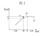
- FIG. 5 is a graph illustrating a method of correcting a voltage level corresponding to a level of maximum luminance by a corrector in FIG. 3 ;
- FIG. 6 is a flowchart illustrating a driving method of the organic light emitting display device according to an embodiment of the present invention.
- first element when a first element is described as being coupled to a second element, the first element may be not only directly coupled to the second element but may also be indirectly coupled to the second element via a third element. Further, some of the elements that are not essential to the complete understanding of the invention are omitted for clarity. Also, like reference numerals refer to like elements throughout.
- FIG. 1 is a graph illustrating a method of determining a level of a power voltage by considering deterioration of a contemporary organic light emitting display device.
- a first curve C 1 indicates relationships between a power voltage of a shipped product, for example, a base power voltage ELVSS and a current I OLED flowing through an organic light emitting diode
- a second curve C 2 indicates relationships between the base power voltage ELVSS and the current I OLED when the organic light emitting display device deteriorates.
- an optimized level of the base power voltage of a shipped product is a first voltage V 1 but a second voltage V 2 is set to the level of the base power voltage by considering deterioration of the organic light emitting display device.
- additional power consumption occurs as much as a difference between the first voltage V 1 and the second voltage V 2 even before the organic light emitting display device is deteriorated.
- FIG. 2 is a graph illustrating a method of determining a power voltage considering a full white pattern in a contemporary organic light emitting display device.
- a third curve C 3 indicates relationships between a base power voltage ELVSS and a current I OLED when an organic light emitting diode emits light in the full white pattern, that is, at the brightest luminance
- a fourth curve C 4 and a fifth curve C 5 indicate relationships between the base power voltage ELVSS and the current I OLED when the organic light emitting diode emits at a normal luminance.
- the contemporary organic light emitting display device supplies a third voltage V 3 as a level of the base power voltage ELVSS by considering the full white pattern regardless of supplying the fourth voltage V 4 or the fifth voltage V 5 as a level of the base power voltage ELVSS in a normal case. By doing so, there occurs an additional power consumption corresponding to a difference between the third voltage V 3 and the fourth voltage V 4 or the fifth voltage V 5 .
- FIG. 3 is a view illustrating an organic light emitting display device according to an embodiment of the present invention and FIG. 4 is a view illustrating an image analyzer in FIG. 3 .
- an organic light emitting display device 100 includes a timing controller 110 , a data driving unit 120 , a scan driving unit 130 , a pixel unit 140 , an image analyzer 150 , a power voltage controller 160 , a lookup table 170 , a power supply 180 , and a corrector 190 .
- the timing controller 110 controls operations of the data driving unit 120 and the scan driving unit 130 and arranges data supplied from the outside again to output the re-arranged data to the data driving unit 120 .
- the timing controller 110 creates a data driving control signal DCS and supply the created data driving control signal DCS to the data driving unit 120 , and creates a scan driving control signal SCS and supplies the created scan driving control signal SCS to the scan driving unit 130 , in response to a synchronization signal supplied from the outside.
- the data driving unit 120 under the control of the timing controller 110 , that is, in response to the data driving control signal DCS outputted from the timing controller 110 , supplies data signals to the pixel unit 140 through the data lines D 1 to Dm.
- the scan driving unit 130 under the control of the timing controller 110 , that is, in response to the scan driving signal SCS outputted from the timing controller 110 , supplies the scan signals to scan lines S 1 to Sn sequentially.
- the pixel unit 140 includes the pixels 141 arranged at every intersection of the data lines D 1 to Dm and the scan lines S 1 to Sn.
- Each of the pixels 141 in response to the scan signals outputted through the scan lines S 1 to Sn, charges the storage capacitors included in the respective pixels 141 with a voltage corresponding to the data signal outputted through the data lines D 1 to Dm.
- the respective pixels 141 generate light of luminance corresponding to the data signals by making current flow corresponding to the charged voltage of the storage capacitor from a first voltage ELVDD to a second voltage ELVSS via an organic light emitting diode.
- the image analyzer 150 receives input image data DATA from the outside to analyze the input unit and a maximum luminance level MLL of the input image to the power voltage controller 160 according to the analyzed results.
- the image analyzer 150 may create a luminance histogram LH of the input image based on the input image data DATA and may extract a maximum luminance level MLL of the input image from the create luminance histogram LH.
- the maximum luminance level MLL refers to a luminance level of a pixel emitting light of the brightest luminance among the input image of one frame.
- the image analyzer 150 estimates power voltage variation of the power voltage ELVDD or ELVSS according to the analyzed results and outputs the estimated power voltage variation PVV to the power voltage controller 160 .
- the image analyzer 150 analyzes luminance level distribution of the remaining pixels excluding a pixel with the maximum luminance level MLL to estimate the power voltage variation PVV of the power voltage ELVDD or ELVSS.
- PVV refers to estimated value of the voltage drop of the power voltage ELVDD or ELVSS according to the rest of pixels excluding the pixel with maximum luminance level MLL.
- the image analyzer 150 when there is one pixel with a luminance level of 15, four pixels with a luminance level of 14, and five pixels with a luminance level of 10 in the input image, the image analyzer 150 outputs the luminance level of 15 as the maximum luminance level MLL and estimates and outputs a power voltage variation PPV corresponding to the four pixels with the luminance level of 14 and the five pixels with the luminance level of 10.
- the image analyzer 150 includes a luminance histogram generator 151 , a maximum luminance level extractor 153 , and a power voltage variation estimator 155 .
- the luminance histogram generator 151 generates a luminance histogram LH for an input image based on the input image data DATA. Specifically, the luminance histogram generator 151 , based on the input image data DATA, counts the number of the pixels every luminance level from an input image of one frame to generate the luminance histogram LH.
- the maximum luminance level extractor 153 extracts the maximum luminance level MLL from the luminance histogram LH outputted from the luminance histogram generator 151 and outputs the extracted maximum luminance level MLL to the power voltage controller 160 .
- the power voltage variation estimator 155 based on the luminance histogram LH, estimates the power voltage variation PVV of the power voltage ELVDD or ELVSS of the remaining pixels excluding the pixels with the maximum luminance level MLL according to the luminance level distribution and outputs the estimated power voltage variation PVV to the power voltage controller 160 .
- the power voltage controller 160 reads a voltage level corresponding to the maximum luminance level MLL outputted from the image analyzer 150 from a lookup table 170 and outputs a power voltage control signal VCS corresponding to the read voltage level to the power supply 180 .
- the power voltage controller 160 regulates the voltage level read from the lookup table 170 corresponding to the power voltage variation PVV outputted from the image analyzer 150 and outputs a power voltage control signal VCS corresponding to the regulated voltage level to the power supply 180 .
- the power voltage controller 160 may output a power voltage control signal VCS corresponding to the voltage level of ⁇ 4.0 V to the power supply 180 .
- the lookup table 170 stores voltage levels corresponding to the luminance levels of the shipped product respectively.
- the data stored in the lookup table 170 may be corrected under the control of the corrector 190 .
- the power supply 180 in response to the power voltage control signal VCS outputted from the power voltage controller 160 , outputs the power voltage ELVDD or ELVSS of the voltage level corresponding to the maximum luminance level MLL to the pixel unit 140 via power lines.
- the corrector 190 senses current flowing through the power lines and corrects the data stored in the lookup table 170 based on the sensed current. Specifically, the corrector 190 , when the current estimated in response to the level of the power voltage ELVDD or ELVSS supplied through the power lines is not equal to the current actually flows through the power lines, corrects the data stored in the lookup table 170 according to the difference.
- the corrector 190 may work only when temperature and an image of the organic light emitting display device 100 are not changed.
- the organic light emitting display device 100 may further include a temperature sensor (not shown).
- the corrector 190 may work only when the temperature or the input image of the organic light emitting display device 100 is not changed so as to prevent malfunctions.
- FIG. 5 is a graph illustrating a method of correcting a voltage level corresponding to the maximum luminance level by the corrector in FIG. 3 .
- a sixth curve C 6 indicates relationships between a power voltage of a shipped product, for example, the base power voltage ELVSS and a current I ELVSS flowing the power lines, for example, base power lines, while a seventh curve C 7 indicates relationships between the base power voltage ELVSS and the current I ELVSS when the organic light emitting display device deteriorates.
- the power supply 180 supplies a sixth voltage V 6 as a voltage level of the base power voltage ELVSS to the base power lines under the control of the power voltage controller 160 .
- a value of the current estimated to flow through the base power lines in corresponding to the sixth voltage V 6 is a first current I 1 .
- a value of the current actually flows through the base power lines is a second current I 2 .
- the corrector 190 correct the data stored in the lookup table 170 into a seventh voltage V 7 based on a difference ⁇ i (I 1 -I 2 ) between the first current I 1 and the second current I 2 .
- the power supply 180 supplies the seventh voltage V 7 as the base power voltage ELVSS.
- FIG. 5 shows the method of correcting a voltage level of the base power voltage ELVSS stored in the lookup table 170 by the corrector 190 , but the spirit of the present invention is not limited thereto. That is, the corrector 190 , similar to the method illustrated in FIG. 5 , may correct the voltage level of the driving power voltage ELVDD stored in the lookup table 170 .
- the organic light emitting display device 100 can regulate a level of the power voltage ELVDD or ELVSS according to deterioration of the organic light emitting display device 100 so that the level of the power voltage ELVDD or ELVSS can be set regardless of taking deterioration of the shipped organic light emitting display device 100 into consideration. Therefore, the power consumption may be reduced before the organic light emitting display device is shipped and deteriorated.
- FIG. 6 is a flowchart illustrating a driving method of the organic light emitting display device according to an embodiment of the present invention.
- the luminance histogram generator 151 generates a luminance histogram LH for the input image based on the input image data DATA (S 100 ).
- the maximum luminance level extractor 153 extracts the maximum luminance level MLL from the luminance histogram LH and the voltage variation estimator 155 estimates the power voltage variation PVV based on the luminance histogram LH. (S 110 and S 120 )
- the power voltage controller 160 outputs the voltage control signal VCS to the power supply 180 , in response to the maximum luminance level MLL and the power voltage variation PVV. That is, the power voltage controller 160 reads a voltage level corresponding to the maximum luminance level MLL from the lookup table 170 (S 130 ), regulates the read voltage level in response to the power voltage variation PVV, and outputs the voltage control signal VCS corresponding to the regulated voltage level to the power supply 180 (S 140 ).
- the power supply 180 in response to the voltage control signal VCS, supplies the power voltage ELVDD or ELVSS to the pixel unit 140 via the power lines (S 150 ).
- the corrector 190 senses a current flowing through the power lines (S 160 ) and compares the sensed current with the estimated current corresponding to the power voltage ELVDD or ELVSS supplied to the power line (S 170 ).
- the corrector 190 determines whether temperature of the organic light emitting display device 100 or the input image is changed (S 180 ).
- the corrector 190 corrects the voltage level corresponding to the maximum luminance level MLL stored in the lookup table 170 based on the difference between the sensed current and the estimated current corresponding to the power voltage ELVDD or ELVSS supplied to the power lines (S 190 ).
Landscapes
- Engineering & Computer Science (AREA)
- Physics & Mathematics (AREA)
- Computer Hardware Design (AREA)
- General Physics & Mathematics (AREA)
- Theoretical Computer Science (AREA)
- Microelectronics & Electronic Packaging (AREA)
- Control Of El Displays (AREA)
- Control Of Indicators Other Than Cathode Ray Tubes (AREA)
- Electroluminescent Light Sources (AREA)
Abstract
Description
- This application makes reference to, incorporates the same herein, and claims all benefits accruing under 35 U.S.C. §119 from an application earlier filed in the Korean Intellectual Property Office on 8 Jan. 2013 and there duly assigned Serial No. 10-2013-0002049.
- 1. Field of the Invention
- An embodiment of the present invention relates to an organic light emitting display device and a method of driving the same, and more particularly, to an organic light emitting display device capable of reducing power consumption by adjusting a voltage according to an input image and deterioration of the organic light emitting display device and a method of driving the same.
- 2. Description of the Related Art
- Recently, various flat panel display devices (FPD) capable of reducing weight and volume that are disadvantages of cathode ray tubes (CRT) have been developed. The FPDs include liquid crystal display devices (LCD), field emission display devices (FED), plasma display panels (PDP), and organic light emitting display devices.
- Among the FPDs, the organic light emitting display devices display images using organic light emitting diodes (OLED) that generate light by re-combination of electrons and holes. The organic light emitting display device has higher response speed and is driven with lower power consumption.
- The contemporary organic light emitting display device includes a data driving unit for supplying data signals to data lines, a scan driving unit for sequentially supplying scan signals to scan lines, a pixel unit having pixels arranged at every intersections between the scan lines, and a timing controller for controlling operations of the data driving unit and the scan driving unit.
- The pixels charge, when the scan signal are supplied, voltage corresponding to the data signals supplied through the data lines storage capacitors included in the respective pixels and supply current corresponding to the charged voltage to organic light emitting diodes to emit light of luminance corresponding to the data signals.
- In the contemporary organic light emitting display device, an optimized level of the base power voltage of a shipped product is a first voltage but a second voltage is set to the level of the base power voltage by considering deterioration of the organic light emitting display device. Thus, additional power consumption occurs as much as a difference between the first voltage and the second voltage even before the organic light emitting display device is deteriorated. The contemporary organic light emitting display device supplies a third voltage as a level of the base power voltage by considering the full white pattern regardless of supplying the fourth voltage or the fifth voltage as a level of the base power voltage in a normal case. By doing so, there occurs an additional power consumption corresponding to a difference between the third voltage and the fourth voltage or the fifth voltage.
- The above information disclosed in this Background section is only for enhancement of understanding of the background of the described technology and therefore it may contain information that does not form the prior art that is already known in this country to a person of ordinary skill in the art.
- Accordingly, the present invention has been made to provide an organic light emitting display device capable of reducing power consumption by regulating a power voltage based on an input image and deterioration of an the organic light emitting display device, and a method of driving the same.
- In order to achieve the foregoing and/or other aspects of the present invention, there is provided an organic light emitting display device including: a pixel unit including pixels arranged at every intersection between data lines and scan lines; a data driving unit supplying a data signal to the data lines; a scan driving unit supplying scan signals to the scan lines sequentially; an image analyzer analyzing an input image and outputting a maximum luminance level of the input image according to the analyzed result; a power voltage controller reading a voltage level corresponding to the maximum luminance level from a lookup table and outputting a power voltage control signal corresponding to the read voltage level; a power supply supplying a power voltage corresponding to the voltage level to the pixel unit via power lines in response to the power voltage control signal; and a corrector correcting the voltage level corresponding to the maximum luminance level stored in the lookup table based on a difference between a current flowing through the power lines and a current estimated in corresponding to the voltage level.
- According to an embodiment of the present invention, the image analyzer may include a luminance histogram generator generating a luminance histogram for the input image, and a maximum luminance level extractor extracting the maximum luminance level from the luminance histogram.
- According to an embodiment of the present invention, the image analyzer may further include a power voltage variation estimator estimating a power voltage variation of the power voltage based on the luminance histogram and outputting the estimated power voltage variation to the power voltage controller.
- According to an embodiment of the present invention, the power voltage controller may regulate and output the power voltage control signal in response to the estimated power voltage variation.
- According to an embodiment of the present invention, the corrector may do not work when temperature of the organic light emitting display device and the input image are changed.
- According to an embodiment of the present invention, the power voltage may be a driving power voltage or a base power voltage.
- Another aspect of the present invention provides a method of driving an organic light emitting display device including: generating a luminance histogram for an input image; extracting a maximum luminance level from the luminance histogram; reading a voltage level corresponding to the maximum luminance level from a lookup table; supplying a power voltage corresponding to the read voltage level to a pixel unit through power lines; and correcting the voltage level corresponding to the maximum luminance level stored in the lookup table according to a difference between a current flowing through the power lines and an estimated current corresponding to the voltage level.
- According to an embodiment of the present invention, the method may further include estimating a power voltage variation of the power voltage based on the luminance histogram.
- According to an embodiment of the present invention, in the supply of the power voltage corresponding to the read voltage level to the pixel unit though the power lines, the voltage level may be regulated in response to the power voltage variation and the power voltage corresponding to the regulated voltage level may be supplied to the pixel unit.
- According to an embodiment of the present invention, correcting the voltage level may include: determining whether temperature of the organic light emitting display device and the input image are changed; and correcting the voltage level corresponding to the maximum luminance level stored in the lookup table based on a difference between a current flowing through the power lines and an estimated current corresponding to the voltage level when the temperature and the input image are not changed as the determined result.
- According to an embodiment of the present invention, correcting the voltage level may further include: sensing a current flowing through the power lines; comparing an estimated current corresponding to the voltage level with the sensed current; and correcting the voltage level corresponding to the maximum luminance level stored in the lookup table when the estimated current corresponding to the voltage level is different from the sensed current according to the compared result.
- According to an embodiment of the present invention, the power voltage may be a driving power voltage or a base power voltage.
- According to the organic light emitting display device according to the present invention and the method of driving the same, the power voltage is regulated based on the input image and deterioration of the organic light emitting display device so that power consumption may be reduced.
- A more complete appreciation of the invention, and many of the attendant advantages thereof, will be readily apparent as the same becomes better understood by reference to the following detailed description when considered in conjunction with the accompanying drawings in which like reference symbols indicate the same or similar components, wherein:
-
FIG. 1 is a graph illustrating a contemporary method of determining a level of a power voltage considering deterioration of a contemporary organic light emitting display device; -
FIG. 2 is a graph illustrating a contemporary method of determining a level of a power consumption considering full white pattern of a contemporary organic light emitting display device; -
FIG. 3 is a view illustrating an organic light emitting display device according to an embodiment of the present invention; -
FIG. 4 is a view illustrating an image analyzer inFIG. 3 ; -
FIG. 5 is a graph illustrating a method of correcting a voltage level corresponding to a level of maximum luminance by a corrector inFIG. 3 ; and -
FIG. 6 is a flowchart illustrating a driving method of the organic light emitting display device according to an embodiment of the present invention. - Hereinafter, certain exemplary embodiments according to the present invention will be described with reference to the accompanying drawings. Here, when a first element is described as being coupled to a second element, the first element may be not only directly coupled to the second element but may also be indirectly coupled to the second element via a third element. Further, some of the elements that are not essential to the complete understanding of the invention are omitted for clarity. Also, like reference numerals refer to like elements throughout.
-
FIG. 1 is a graph illustrating a method of determining a level of a power voltage by considering deterioration of a contemporary organic light emitting display device. - In reference to
FIG. 1 , a first curve C1 indicates relationships between a power voltage of a shipped product, for example, a base power voltage ELVSS and a current IOLED flowing through an organic light emitting diode, while a second curve C2 indicates relationships between the base power voltage ELVSS and the current IOLED when the organic light emitting display device deteriorates. - In the contemporary organic light emitting display device, an optimized level of the base power voltage of a shipped product is a first voltage V1 but a second voltage V2 is set to the level of the base power voltage by considering deterioration of the organic light emitting display device. Thus, additional power consumption occurs as much as a difference between the first voltage V1 and the second voltage V2 even before the organic light emitting display device is deteriorated.
-
FIG. 2 is a graph illustrating a method of determining a power voltage considering a full white pattern in a contemporary organic light emitting display device. - In reference to
FIG. 2 , a third curve C3 indicates relationships between a base power voltage ELVSS and a current IOLED when an organic light emitting diode emits light in the full white pattern, that is, at the brightest luminance, while a fourth curve C4 and a fifth curve C5 indicate relationships between the base power voltage ELVSS and the current IOLED when the organic light emitting diode emits at a normal luminance. - The contemporary organic light emitting display device supplies a third voltage V3 as a level of the base power voltage ELVSS by considering the full white pattern regardless of supplying the fourth voltage V4 or the fifth voltage V5 as a level of the base power voltage ELVSS in a normal case. By doing so, there occurs an additional power consumption corresponding to a difference between the third voltage V3 and the fourth voltage V4 or the fifth voltage V5.
- Hereinafter, an organic light emitting display device according to an embodiment of the present invention and a method of driving the same will be described in detail as follows with reference to the accompanying drawings.
-
FIG. 3 is a view illustrating an organic light emitting display device according to an embodiment of the present invention andFIG. 4 is a view illustrating an image analyzer inFIG. 3 . - In reference to
FIG. 3 , an organic lightemitting display device 100 includes atiming controller 110, adata driving unit 120, ascan driving unit 130, apixel unit 140, animage analyzer 150, apower voltage controller 160, a lookup table 170, apower supply 180, and acorrector 190. - The
timing controller 110 controls operations of thedata driving unit 120 and thescan driving unit 130 and arranges data supplied from the outside again to output the re-arranged data to thedata driving unit 120. - Specifically, the
timing controller 110 creates a data driving control signal DCS and supply the created data driving control signal DCS to thedata driving unit 120, and creates a scan driving control signal SCS and supplies the created scan driving control signal SCS to thescan driving unit 130, in response to a synchronization signal supplied from the outside. - The
data driving unit 120, under the control of thetiming controller 110, that is, in response to the data driving control signal DCS outputted from thetiming controller 110, supplies data signals to thepixel unit 140 through the data lines D1 to Dm. - The
scan driving unit 130, under the control of thetiming controller 110, that is, in response to the scan driving signal SCS outputted from thetiming controller 110, supplies the scan signals to scan lines S1 to Sn sequentially. - The
pixel unit 140 includes thepixels 141 arranged at every intersection of the data lines D1 to Dm and the scan lines S1 to Sn. Each of thepixels 141, in response to the scan signals outputted through the scan lines S1 to Sn, charges the storage capacitors included in therespective pixels 141 with a voltage corresponding to the data signal outputted through the data lines D1 to Dm. Therespective pixels 141 generate light of luminance corresponding to the data signals by making current flow corresponding to the charged voltage of the storage capacitor from a first voltage ELVDD to a second voltage ELVSS via an organic light emitting diode. - The
image analyzer 150 receives input image data DATA from the outside to analyze the input unit and a maximum luminance level MLL of the input image to thepower voltage controller 160 according to the analyzed results. For example, theimage analyzer 150 may create a luminance histogram LH of the input image based on the input image data DATA and may extract a maximum luminance level MLL of the input image from the create luminance histogram LH. Here, the maximum luminance level MLL refers to a luminance level of a pixel emitting light of the brightest luminance among the input image of one frame. - Moreover, the
image analyzer 150 estimates power voltage variation of the power voltage ELVDD or ELVSS according to the analyzed results and outputs the estimated power voltage variation PVV to thepower voltage controller 160. Specifically, theimage analyzer 150 analyzes luminance level distribution of the remaining pixels excluding a pixel with the maximum luminance level MLL to estimate the power voltage variation PVV of the power voltage ELVDD or ELVSS. PVV refers to estimated value of the voltage drop of the power voltage ELVDD or ELVSS according to the rest of pixels excluding the pixel with maximum luminance level MLL. - For example, when there is one pixel with a luminance level of 15, four pixels with a luminance level of 14, and five pixels with a luminance level of 10 in the input image, the
image analyzer 150 outputs the luminance level of 15 as the maximum luminance level MLL and estimates and outputs a power voltage variation PPV corresponding to the four pixels with the luminance level of 14 and the five pixels with the luminance level of 10. - In reference to
FIG. 4 , theimage analyzer 150 includes aluminance histogram generator 151, a maximumluminance level extractor 153, and a powervoltage variation estimator 155. - The
luminance histogram generator 151 generates a luminance histogram LH for an input image based on the input image data DATA. Specifically, theluminance histogram generator 151, based on the input image data DATA, counts the number of the pixels every luminance level from an input image of one frame to generate the luminance histogram LH. - The maximum
luminance level extractor 153 extracts the maximum luminance level MLL from the luminance histogram LH outputted from theluminance histogram generator 151 and outputs the extracted maximum luminance level MLL to thepower voltage controller 160. - The power
voltage variation estimator 155, based on the luminance histogram LH, estimates the power voltage variation PVV of the power voltage ELVDD or ELVSS of the remaining pixels excluding the pixels with the maximum luminance level MLL according to the luminance level distribution and outputs the estimated power voltage variation PVV to thepower voltage controller 160. - The
power voltage controller 160 reads a voltage level corresponding to the maximum luminance level MLL outputted from theimage analyzer 150 from a lookup table 170 and outputs a power voltage control signal VCS corresponding to the read voltage level to thepower supply 180. - According to an embodiment, the
power voltage controller 160 regulates the voltage level read from the lookup table 170 corresponding to the power voltage variation PVV outputted from theimage analyzer 150 and outputs a power voltage control signal VCS corresponding to the regulated voltage level to thepower supply 180. - For example, when the level of the base power voltage corresponding to the maximum luminance level MLL is −3.0 V and the power voltage variation PVV indicates −1.0 V, the
power voltage controller 160 may output a power voltage control signal VCS corresponding to the voltage level of −4.0 V to thepower supply 180. - The lookup table 170 stores voltage levels corresponding to the luminance levels of the shipped product respectively. The data stored in the lookup table 170 may be corrected under the control of the
corrector 190. - The
power supply 180, in response to the power voltage control signal VCS outputted from thepower voltage controller 160, outputs the power voltage ELVDD or ELVSS of the voltage level corresponding to the maximum luminance level MLL to thepixel unit 140 via power lines. - The
corrector 190 senses current flowing through the power lines and corrects the data stored in the lookup table 170 based on the sensed current. Specifically, thecorrector 190, when the current estimated in response to the level of the power voltage ELVDD or ELVSS supplied through the power lines is not equal to the current actually flows through the power lines, corrects the data stored in the lookup table 170 according to the difference. - The
corrector 190 may work only when temperature and an image of the organic light emittingdisplay device 100 are not changed. To this end, the organic light emittingdisplay device 100 may further include a temperature sensor (not shown). - When temperature or the input image of the organic light emitting
display device 100 are changed, the voltage level of the power voltage ELVDD or ELVSS and/or the current flowing through the power lines may vary. Thus, thecorrector 190 may work only when the temperature or the input image of the organic light emittingdisplay device 100 is not changed so as to prevent malfunctions. -
FIG. 5 is a graph illustrating a method of correcting a voltage level corresponding to the maximum luminance level by the corrector inFIG. 3 . - In reference to
FIG. 5 , a sixth curve C6 indicates relationships between a power voltage of a shipped product, for example, the base power voltage ELVSS and a current IELVSS flowing the power lines, for example, base power lines, while a seventh curve C7 indicates relationships between the base power voltage ELVSS and the current IELVSS when the organic light emitting display device deteriorates. - The
power supply 180 supplies a sixth voltage V6 as a voltage level of the base power voltage ELVSS to the base power lines under the control of thepower voltage controller 160. In this case, a value of the current estimated to flow through the base power lines in corresponding to the sixth voltage V6 is a first current I1. However, due to the deterioration of the organic light emittingdisplay device 100, a value of the current actually flows through the base power lines is a second current I2. - In this case, the
corrector 190 correct the data stored in the lookup table 170 into a seventh voltage V7 based on a difference Δi (I1-I2) between the first current I1 and the second current I2. After that, thepower supply 180 supplies the seventh voltage V7 as the base power voltage ELVSS. -
FIG. 5 shows the method of correcting a voltage level of the base power voltage ELVSS stored in the lookup table 170 by thecorrector 190, but the spirit of the present invention is not limited thereto. That is, thecorrector 190, similar to the method illustrated inFIG. 5 , may correct the voltage level of the driving power voltage ELVDD stored in the lookup table 170. - The organic light emitting
display device 100 according to an embodiment of the present invention can regulate a level of the power voltage ELVDD or ELVSS according to deterioration of the organic light emittingdisplay device 100 so that the level of the power voltage ELVDD or ELVSS can be set regardless of taking deterioration of the shipped organic light emittingdisplay device 100 into consideration. Therefore, the power consumption may be reduced before the organic light emitting display device is shipped and deteriorated. -
FIG. 6 is a flowchart illustrating a driving method of the organic light emitting display device according to an embodiment of the present invention. - In reference to
FIG. 6 , theluminance histogram generator 151 generates a luminance histogram LH for the input image based on the input image data DATA (S100). The maximumluminance level extractor 153 extracts the maximum luminance level MLL from the luminance histogram LH and thevoltage variation estimator 155 estimates the power voltage variation PVV based on the luminance histogram LH. (S110 and S120) - The
power voltage controller 160 outputs the voltage control signal VCS to thepower supply 180, in response to the maximum luminance level MLL and the power voltage variation PVV. That is, thepower voltage controller 160 reads a voltage level corresponding to the maximum luminance level MLL from the lookup table 170 (S130), regulates the read voltage level in response to the power voltage variation PVV, and outputs the voltage control signal VCS corresponding to the regulated voltage level to the power supply 180 (S140). - The
power supply 180, in response to the voltage control signal VCS, supplies the power voltage ELVDD or ELVSS to thepixel unit 140 via the power lines (S150). Thecorrector 190 senses a current flowing through the power lines (S160) and compares the sensed current with the estimated current corresponding to the power voltage ELVDD or ELVSS supplied to the power line (S170). - When the sensed current is not equal to the estimated current corresponding to the voltage level, the
corrector 190 determines whether temperature of the organic light emittingdisplay device 100 or the input image is changed (S180). - According to the determination, when the temperature of the organic light emitting
display device 100 or the input image is not changed, thecorrector 190 corrects the voltage level corresponding to the maximum luminance level MLL stored in the lookup table 170 based on the difference between the sensed current and the estimated current corresponding to the power voltage ELVDD or ELVSS supplied to the power lines (S190). - While the present invention has been described in connection with certain exemplary embodiments, it is to be understood that the invention is not limited to the disclosed embodiments, but, on the contrary, is intended to cover various modifications and equivalent arrangements included within the spirit and scope of the appended claims, and equivalents thereof.
Claims (12)
Applications Claiming Priority (2)
| Application Number | Priority Date | Filing Date | Title |
|---|---|---|---|
| KR10-2013-0002049 | 2013-01-08 | ||
| KR1020130002049A KR102061849B1 (en) | 2013-01-08 | 2013-01-08 | Organic light emitting display and method for driving the same |
Publications (2)
| Publication Number | Publication Date |
|---|---|
| US20140191663A1 true US20140191663A1 (en) | 2014-07-10 |
| US9241387B2 US9241387B2 (en) | 2016-01-19 |
Family
ID=51060473
Family Applications (1)
| Application Number | Title | Priority Date | Filing Date |
|---|---|---|---|
| US14/032,684 Active 2033-12-14 US9241387B2 (en) | 2013-01-08 | 2013-09-20 | Organic light emitting display device and method of driving the same |
Country Status (2)
| Country | Link |
|---|---|
| US (1) | US9241387B2 (en) |
| KR (1) | KR102061849B1 (en) |
Cited By (2)
| Publication number | Priority date | Publication date | Assignee | Title |
|---|---|---|---|---|
| CN113053294A (en) * | 2019-12-27 | 2021-06-29 | 三星显示有限公司 | Optical compensation system and optical compensation method of display device |
| US11081053B2 (en) * | 2019-01-28 | 2021-08-03 | Apple Inc. | Electronic devices having displays with compensation for oxide transistor threshold voltage |
Families Citing this family (2)
| Publication number | Priority date | Publication date | Assignee | Title |
|---|---|---|---|---|
| JP6853750B2 (en) * | 2017-08-10 | 2021-03-31 | 株式会社Joled | Luminance control device, light emitting device and brightness control method |
| KR102350724B1 (en) * | 2017-08-21 | 2022-01-13 | 삼성전자주식회사 | A method and an electronic device for switching operating mode of an display |
Citations (4)
| Publication number | Priority date | Publication date | Assignee | Title |
|---|---|---|---|---|
| US8451208B2 (en) * | 2008-03-03 | 2013-05-28 | Samsung Display Co., Ltd. | Organic light emitting display device and method of driving the same |
| US8937585B2 (en) * | 2010-07-27 | 2015-01-20 | Samsung Display Co., Ltd. | Pixel and organic light emitting display using the same |
| US9007355B2 (en) * | 2011-10-31 | 2015-04-14 | Lg Display Co., Ltd. | Organic light emitting display |
| US9041626B2 (en) * | 2007-10-29 | 2015-05-26 | Samsung Display Co., Ltd. | Organic light emitting display and power supply method thereof |
Family Cites Families (4)
| Publication number | Priority date | Publication date | Assignee | Title |
|---|---|---|---|---|
| KR100748739B1 (en) | 2005-01-28 | 2007-08-13 | 도시바 마쯔시따 디스플레이 테크놀로지 컴퍼니, 리미티드 | El display apparatus and method of driving the same |
| JP2008292649A (en) * | 2007-05-23 | 2008-12-04 | Hitachi Displays Ltd | Image display device |
| KR101065320B1 (en) * | 2010-02-24 | 2011-09-16 | 삼성모바일디스플레이주식회사 | Organic light emitting display device and driving method thereof |
| JP5499872B2 (en) * | 2010-04-21 | 2014-05-21 | ソニー株式会社 | Battery control device, battery control method and program |
-
2013
- 2013-01-08 KR KR1020130002049A patent/KR102061849B1/en active Active
- 2013-09-20 US US14/032,684 patent/US9241387B2/en active Active
Patent Citations (4)
| Publication number | Priority date | Publication date | Assignee | Title |
|---|---|---|---|---|
| US9041626B2 (en) * | 2007-10-29 | 2015-05-26 | Samsung Display Co., Ltd. | Organic light emitting display and power supply method thereof |
| US8451208B2 (en) * | 2008-03-03 | 2013-05-28 | Samsung Display Co., Ltd. | Organic light emitting display device and method of driving the same |
| US8937585B2 (en) * | 2010-07-27 | 2015-01-20 | Samsung Display Co., Ltd. | Pixel and organic light emitting display using the same |
| US9007355B2 (en) * | 2011-10-31 | 2015-04-14 | Lg Display Co., Ltd. | Organic light emitting display |
Cited By (2)
| Publication number | Priority date | Publication date | Assignee | Title |
|---|---|---|---|---|
| US11081053B2 (en) * | 2019-01-28 | 2021-08-03 | Apple Inc. | Electronic devices having displays with compensation for oxide transistor threshold voltage |
| CN113053294A (en) * | 2019-12-27 | 2021-06-29 | 三星显示有限公司 | Optical compensation system and optical compensation method of display device |
Also Published As
| Publication number | Publication date |
|---|---|
| KR20140089945A (en) | 2014-07-16 |
| US9241387B2 (en) | 2016-01-19 |
| KR102061849B1 (en) | 2020-01-03 |
Similar Documents
| Publication | Publication Date | Title |
|---|---|---|
| US9430965B2 (en) | Organic light emitting display device and driving method thereof | |
| US9691323B2 (en) | Organic light emitting display and method of driving the same | |
| EP2282307B1 (en) | Organic light emitting display device and driving voltage setting method thereof | |
| JP6773632B2 (en) | Display panel and electroluminescent display | |
| US9240142B2 (en) | Apparatus and method for driving organic light emitting display device | |
| US10062324B2 (en) | Luminance control device and display device comprising the same | |
| KR101983764B1 (en) | Organic light emitting display and method for driving the same | |
| US9478156B2 (en) | Organic light emitting display device and driving method thereof | |
| US9147360B2 (en) | Apparatus and method for driving of organic light emitting display device | |
| US9508284B2 (en) | Method of driving organic electroluminescent display device | |
| US9898961B2 (en) | Data processing method and apparatus for organic light emitting diode display device | |
| US20130002960A1 (en) | Signal Controller For Display Device, Display Device, And Driving Method Thereof | |
| US8912987B2 (en) | Organic light emitting display device and driving method thereof | |
| US9330595B2 (en) | Organic light emitting display device and driving method thereof | |
| KR101928018B1 (en) | Pixel and Organic Light Emitting Display Device Using the same | |
| US20140292821A1 (en) | Display device | |
| US20140021870A1 (en) | Organic light emitting display and method of driving the same | |
| US11574601B2 (en) | Display device and method for controlling display device | |
| US9241387B2 (en) | Organic light emitting display device and method of driving the same | |
| US20140354703A1 (en) | Organic light emitting display device and driving method thereof | |
| US9099035B2 (en) | Organic light emitting display and method of driving the same | |
| US20140118410A1 (en) | Organic light emitting diode display and driving method thereof | |
| US20120062623A1 (en) | Organic light emitting display and method of driving the same | |
| KR20160058574A (en) | Organic light emmitting diode display device and driving method thereof | |
| KR102153392B1 (en) | Organic light emitting display device and method for driving thereof |
Legal Events
| Date | Code | Title | Description |
|---|---|---|---|
| AS | Assignment |
Owner name: SAMSUNG DISPLAY CO., LTD., KOREA, REPUBLIC OF Free format text: ASSIGNMENT OF ASSIGNORS INTEREST;ASSIGNORS:SHIN, JEONG-HWAN;LEE, WOOK;CHAE, SE-BYUNG;REEL/FRAME:031903/0048 Effective date: 20130723 |
|
| STCF | Information on status: patent grant |
Free format text: PATENTED CASE |
|
| MAFP | Maintenance fee payment |
Free format text: PAYMENT OF MAINTENANCE FEE, 4TH YEAR, LARGE ENTITY (ORIGINAL EVENT CODE: M1551); ENTITY STATUS OF PATENT OWNER: LARGE ENTITY Year of fee payment: 4 |
|
| MAFP | Maintenance fee payment |
Free format text: PAYMENT OF MAINTENANCE FEE, 8TH YEAR, LARGE ENTITY (ORIGINAL EVENT CODE: M1552); ENTITY STATUS OF PATENT OWNER: LARGE ENTITY Year of fee payment: 8 |